LatticeECP3™ Video Protocol Board – Revision C
User’s Guide
October 2012
Revision: EB52_01.3
�LatticeECP3 Video Protocol Board – Revision C
User’s Guide
Introduction
The LatticeECP3™ FPGA family includes many features for video applications. For example, DisplayPort, SMPTE
standards (SD-SDI, HD-SDI and 3G-SDI), DVB-ASI, DVI and HDMI can be implemented with 16 channels of
embedded SERDES/PCS. 7:1 LVDS video interfaces like ChannelLink and CameraLink can be supported by the
generic DDRX2 mode on the I/O pins. When configuring to TRLVDS mode, the I/O pins on banks 0 and 1 can also
be used to receive the TMDS signals of DVI or HDMI video standard.
This user’s guide describes revision C of the LatticeECP3 Video Protocol Board featuring the LatticeECP3 LFE395E-7FN1156C FPGA device. The stand-alone evaluation PCB provides a functional platform for development and
rapid prototyping of many different video applications.
Figure 1. LatticeECP3 Video Protocol Board – Revision C
Features
• Video interfaces for interconnection to video standard equipment
• Allow the demonstration of SD/HD/3G-SDI, DisplayPort and PCI Express (x4) interfaces using SERDES channels
• High speed Mezzanine connector connected to SERDES channels for future expansion
• Allows the demonstration of LVDS video standards – ChannelLink and CameraLink
• Allows control of SERDES PCS registers using the Serial Client Interface (ORCAstra)
• Allows the demonstration of receiving TMDS signals using the DVI interface
• On-board Boot Flash with Serial SPI Flash memory device
• Shows interoperation with high performance DDR2 memory components
• Driver-based “run-time” device configuration capability via an ORCAstra or RS232 interface
• SMAs for external high-speed clock / PLL inputs
• Switches, LEDs and LCD display header for demo purposes
• Mictor connector for using Logic Analyzer in the debugging phase
2
�LatticeECP3 Video Protocol Board – Revision C
User’s Guide
• Input connection for lab-power supply
• Power connections and power sources
• ispVM™ programming support
• On-board and external reference clock sources
• Various high-speed layout structures
• User-defined input and output points
• Performance monitoring via test headers, LEDs and switches
The contents of this user’s guide include top-level functional descriptions of the various portions of the evaluation
board, descriptions of the on-board connectors, diodes and switches and a complete set of schematics of the
board. Figure 2 shows the functional partitioning of the board.
Figure 2. LatticeECP3 Video Protocol Board – Revision C Functional Partition
PCI Express
x4 Edge
DDR2
Memory
Tx Refclk Generation Circuitry
27MHz
DDR2
Memory
VCO
Bank 6
GS4915
Ch3
Ch2
Ch1
DisplayPort
Tx
Bank 7
Quad C
Refclk
GS4911
Ch0
Bank 0
DisplayPort
Rx
Ch3
Ch2
Ch1
Quad B
Refclk
SERDES LatticeECP3-95
1156 fpBGA
Ch0
3G-SDI
Driver
SDI
Rx #1
3G-SDI
Equalizer
Bank 1
Refclk
Ch3
Ch2
Ch1
DVI
Tx
Quad A
SDI
Tx #1
Bank 3
Ch0
3G-SDI
Driver
3G-SDI
Equalizer
ChannelLink
Tx
SDI
Tx #0
Bank 2
from internal PLL(s)
ChannelLink
Rx
RJ45
Tx/Rx
CameraLink
Rx
DVI
Rx
SDI
Rx #0
Differences Between the Revision B and Revision C Boards
The major changes in revision C are summarized below:
1. The Revision C board includes eight pull-up resistors, R362-R369, to the DVI Rx signals placed close to the
LatticeECP3 device. These resistors are used for termination of the DVI’s TMDS signals and are not included
on the Revision B board.
3
�LatticeECP3 Video Protocol Board – Revision C
User’s Guide
2. The Revision C board includes eight pull-up resistors, R370-R377, to the DDR2 memory’s DQS signals. These
resistors are placed close to the LatticeECP3 device. These resistors are not included on the Revision B board.
3. The Revision C board includes R75 between the P and N reference clocks of SERDES Quad C (Mezzanine
daughter board) for future use. No resistor is populated. This resistor is not included on the Revision B board.
4. On the Revision C board, the Gennum clock generators (GS4911) on U2 and U3 are not populated.
LatticeECP3 Device
This board features a LatticeECP3 FPGA with a 1.2V core supply. It can accommodate all pin compatible
LatticeECP3 devices in the 1156-ball fpBGA (1mm pitch) package. A complete description of this device can be
found in the LatticeECP3 Family Data Sheet.
Applying Power to the Board
The LatticeECP3 Video Protocol Board is ready to power on. This board can be supplied with power from an AC
wall-type transformer power supply shipped with the board. Or it can be supplied from a bench top supply via terminal screw connections. It also has provisions to be supplied from the PCI Express edge fingers from a host board.
To supply power from the factory-supplied wall transformer, simply connect the output connection of the power cord
to J15 and plug wall-transformer into an AC wall outlet.
Supply Power from Bench Power Supply
The evaluation board incorporates an alternate scheme to provide power to the board. The board is equipped to
accept a main supply via the TB1 connection. This connection is intended to be used with a bench top supply
adjusted to provide a nominal 12V DC.
All input power sources and on-board power supplies are fused with surface mounted fuses. Table 1 shows these
fuses and the corresponding powers.
Table 1. Board Power Supply Fuses
Fuse #
Rating
Voltage
F1
3A
2.5V
F2
3A
1.8V
Bank 6, Bank 7 I/Os, DDR2 regulator, DDR2 memory, Gennum clock chips
3A
5.0V
Cable driver/equalizer power regulator, Gennum clock chips power regulators, DisplayPort power output regulators, Mezzanine connector, DVI power output for EDID,
LCD module
F4
3A
1.2V
LatticeECP3 SERDES
F5
10A
12V
Main power supply
F6
10A
1.2V
LatticeECP3 Core
3.3V
LatticeECP3 VCCAUX, PLL, JTAG, Bank 0 and 8 I/Os, SPI Flash memory, push-button
debouncer, DVI transmitter, RS-232 driver/receiver, zero delay clock buffer, clock
oscillators, MachXO™, cable driver/equalizer
F3
F7
10A
Usage
EEPROM, DDR2 regulator, Bank 1, 2 and 3 I/Os, DIP switches
The Lattice ispPAC® Power Manager II device, the ispPAC-POWR1220AT8, is used for monitoring various voltages
on the board. There are six LEDs used to indicate the status of the monitoring voltages. If the monitoring voltage is
not in the +/- 5% voltage window, the corresponding LED will flash; otherwise, the LED will stay ON. Table 2 shows
these six voltages and the corresponding LEDs.
4
�LatticeECP3 Video Protocol Board – Revision C
User’s Guide
Table 2. Board Power Supply Monitoring Indicators
Power
LED #
Voltage Range
In Range
Out of Range
LatticeECP3 SERDES
D33
1.2V +/- 5%
On
Flash
LatticeECP3 Core
D32
1.2V +/- 5%
On
Flash
3.3V
D31
3.3V +/- 5%
On
Flash
2.5V
D29
2.5V +/- 5%
On
Flash
5.0V
D28
5.0V +/- 5%
On
Flash
1.8V
D27
1.8V +/- 5%
On
Flash
External power can be alternatively connected through TB1 rather than the wall transformer power pack.
Table 3. Board Supply Disconnects
Screw terminal for 12V DC
+12V: Pin1 (closer to the wall transformer power jack J15) 12V DC
GND: Pin2 (closer to the LCD connector)
TB1
PCI Express Power Interface
Power can be sourced to the board via the PCB edge-finger (CN1). This interface allows the user to provide power
from a PCI Express host board.
Configuration/Programming Headers
Two programming headers are provided on the board for accessing to the LatticeECP3 JTAG port and sysCONFIG™ port. The JTAG connector is a 1x10 header and the sysCONFIG connector is a 2x17 header.
Table 4. sysCONFIG Connector Pinout (J37)
Net Name
LatticceECP3 Pin
Header Pin
Net Name
CCLK
SISPI
LatticceECP3 Pin
Header Pin
C34
1
GND
—
2
F33
3
D6
J34
4
CSSPI0N
D34
5
3.3V
—
6
CSSP1N
E34
7
INITN
C33
8
DONE
G31
9
PROGRAMN
B34
10
D7
F32
11
GND
—
12
D6
J34
13
GND
—
14
D5
H34
15
GND
—
16
D4
G32
17
GND
—
18
D3
G33
19
GND
—
20
D2
H33
21
GND
—
22
D1
G34
23
GND
—
24
D0
E32
25
GND
—
26
CSN
F31
27
WRITE
E31
28
CS1
G30
29
CFG0
B33
30
3.3V
—
31
CFG1
F30
32
GND
—
33
CFG2
D32
34
J28 is a 10-pin JTAG connector used in conjunction with the ispVM download cable to program and control the Lattice devices on this board.
5
�LatticeECP3 Video Protocol Board – Revision C
User’s Guide
Table 5. ispVM JTAG Connector (J28)
Pin #
Description
Pin 1
VCC
Pin 2
TDO
Pin 3
TDI
Pin 4
PROGRAMN
Pin 5
NC
Pin 6
TMS
Pin 7
GND
Pin 8
TCK
Pin 9
DONE
Pin 10
INITN
This board includes three Lattice programmable devices that can be programmed in a daisy chain (U30 =
LatticeECP3-95, U1 = MachXO™ LCMXO256, and U36 = ispPAC-POWR1220AT8). Other than the LatticeECP395, the JTAG connector provides access to the JTAG ports of the ispPAC-POWR1220AT8 and the MachXO. With
proper jumper selection, the JTAG ports of these devices can be chained together for programming. Table 6 shows
the jumper settings of J32, J33 and J34 used to configure the JTAG connections.
Table 6. JTAG Connection Settings (J32, J33, J34)
Jumper Settings
JTAG Connection
J32 J33 J34
TDI
ECP3
MachXO
ispPAC
1
TDO
J32 J33 J34
TDI
ECP3
MachXO
ispPAC
2
TDO
J32 J33 J34
TDI
TDO
3
ECP3
J32 J33 J34
MachXO
ispPAC
MachXO
ispPAC
TDI
ECP3
4
TDO
6
�LatticeECP3 Video Protocol Board – Revision C
User’s Guide
Table 6. JTAG Connection Settings (J32, J33, J34) (Continued)
Jumper Settings
JTAG Connection
J32 J33 J34
TDI
ECP3
MachXO
ispPAC
ECP3
MachXO
ispPAC
5
TDO
TDI
J32 J33 J34
6
TDO
J32 J33 J34
TDI
ECP3
7
MachXO
ispPAC
TDO
There are several LEDs on the board to indicate the LatticeECP3 programming status. They are listed in Table 7.
Table 7. LED Indicators for Configuration Status
LED #
Color
Function
LED illuminated to indicate that the programming was aborted or reinitialized driving the INITN
output low.
D19
Red
D18
Green
D20
Red
LED illuminated to indicate that PROGRAMN is low.
D21
Red
LED illuminated to indicate that GSRN is low.
LED illuminated to indicate the successful completion of configuration by releasing the open collector DONE output pin.
The PROGRAMN pin of the LatticeECP3-95 is connected to a push-button switch (SW5). Depressing this button
drives a logic level “0” to the PROGRAMN pin. This will force the LatticeECP3 into the configuration mode and initiate the configuration sequence.
The FPGA CFG pins are set on the board for a particular programming mode via the SW2 DIP switch. JTAG programming is independent of the MODE pins and is always available to the user. Pushing down the switch will turn it
on and set the CFG value to 0.
Table 8. CFG Mode Selections
CFG2
(SW2-1)
CFG1
(SW2-2)
CFG0
(SW2-3)
0 (ON)
0 (ON)
0 (ON)
SPI Flash Mode (available on-board)
0 (ON)
1 (OFF)
0 (ON)
SPIm
Selected Configuration Mode
1 (OFF)
0 (ON)
0 (ON)
Master Serial
1 (OFF)
0 (ON)
1 (OFF)
Slave Serial
1 (OFF)
1 (OFF)
0 (ON)
Master Parallel
1 (OFF)
1 (OFF)
1 (OFF)
Slave Parallel
7
�LatticeECP3 Video Protocol Board – Revision C
User’s Guide
On-Board Flash Memory
One SPI (16-pin TSSOP 64M) Flash memory device (U32) is on board for non-volatile configuration memory storage. The CFG [2:0] setting must be [000] for the LatticeECP3 to enable the SPI Flash mode.
Video Clock Management and SDI Cable Driver/Equalizer
Industry standard video clocks are generated and managed via Gennum chipsets. These chipsets are used to generate both transmit and receive reference clocks for LatticeECP3 SERDES. The GS4911 clock generator device
produces multiple video standard reference clocks from an on-board 27MHz crystal. The GS4915 clock cleaner is
used to reduce clock jitter to produce a clean clock for video signal quality using a high-performance VCO. The
Gennum clock devices are used to generate clocks for SD/HD/3G-SDI applications. Since the PLL in LatticeECP3
FPGAs is designed to support all the frequencies required by SD/HD/3G-SDI, the GS4911 clock generator is no
longer needed. The two GS4911 devices found on the Revision B board are included on the Revision C board but
not populated.
Two cable drivers and two cable equalizers are placed on-board for SD/HD/3G-SDI applications that require delivering video signal over 75 ohm coaxial cable.
The control and status pins of the Gennum chipsets and the cable drivers/equalizers are connected to the MachXO
I/O pins. By using the signals connected between the MachXO and LatticeECP3, the Gennum chipsets and cable
drivers/equalizers can be controlled from the design in the LatticeECP3. Figure 3 shows the block diagram of the
control/status buses of the connections between these devices. The MachXO pins connected to these devices are
shown in Tables 9 to 12.
Figure 3. Block Diagram of Gennum Chipsets and Cable Driver/Equalizer Controls
RX_GS4911_RESETn
SDI Tx #1
Cable
Driver
(U24)
SDI Rx #1
Cable
Equalizer
(U21)
Rx Refclk
Generator
GS4911
(U2)
Rx Refclk
Cleaner
GS4915
(U6)
MachXO
SDI Tx #0
Cable
Driver
(U22)
SDI Rx #0
Cable
Equalizer
(U25)
Tx Refclk
Generator
GS4911
(U3)
12
Tx Refclk
Cleaner
GS4915
(U7)
TX_GS4911_RESETn
8
LatticeECP3
�LatticeECP3 Video Protocol Board – Revision C
User’s Guide
Table 9. MachXO Pin Connections to GS4911 Devices (GS4911 Devices are Not Populated on the Revision
C Board)
Signal Type
Control
GS4911 Pin Name
U2 (for Rx Refclk)
U3 (for Tx Refclk)
Pull-low/high
VID_STD0
K2
G13
High
VID_STD1
L1
H13
Low
VID_STD2
L2
J13
High
VID_STD3
M1
J14
Low
VID_STD4
M2
K13
High
VID_STD5
N1
K14
Low
/GENLOCK
M3
M13
High
ASR_SEL0
H2
—
Low
ASR_SEL1
G2
—
Low
ASR_SEL2
F2
—
Low
JTAG / HOSTn
N11
N11
—
SCLK_TCLK1
P13
P13
—
1
SDIN_TDI
SDOUT_TDO
CSn_TMS
/RESET
Status
—
N12
—
P12
—
—
P11
P14
D17 (from LatticeECP3) D12 (from LatticeECP3)
—
Low
LOCK_LOST
—
L14
—
REF_LOST
—
L13
—
TIMING_OUT_1
K1
F14
—
TIMING_OUT_2
J2
F13
—
TIMING_OUT_3
J1
E14
—
TIMING_OUT_4
—
E13
—
1. These are the signals controlled by the same MachXO I/O pins.
Table 10. MachXO Pin Connections to GS4915 Devices
Signal Type
Control
Status
GS4915 Pin Name
U6 (for Rx Refclk)
U7 (for Tx Refclk)
Pull-low/high
/RESET
F1
D14
High
IPSEL
E2
D13
Low
BYPASS
E1
C14
Low
/AUTOBYPASS
C2
C13
Low
FCTRL0
D1
B14
Low
FCTRL1
D2
C12
Low
DOUBLE
C1
A13
Low
SKEW_EN
B1
A12
Low
LOCK
B11
B12
—
Table 11. MachXO Pin Connections to LMH0303 or GS2978 Cable Driver Devices
Signal Type
Control
Status
Driver Pin Name
U22 (for Tx #0)
U24 (for Tx #1)
Pull-low/high
SD / HDn
N5
N14
Low
ENABLE (/DISABLE)
N6
M14
High
/RSTI
N7
—
High
/FAULT
N13
N13
—
9
�LatticeECP3 Video Protocol Board – Revision C
User’s Guide
Table 12. MachXO Pin Connections GS2974 Cable Equalizer Devices
Signal Type
Driver Pin Name
Control
Status
U25 (for Rx #0)
U21 (for Rx #1)
Pull-low/high
BYPASS
P3
P8
Low
MUTE
P4
N8
Low
MCLADJ
Controlled by
potentiometer VR3
Controlled by
potentiometer VR2
—
/CD
N3
P9
—
Table 13. MachXO Pin Connections to LatticeECP3
Net Name
MachXO Pin
LatticeECP3 Pin
ECP3_XO_SIG0
B10
AM31
ECP3_XO_SIG1
A9
AL31
ECP3_XO_SIG2
A7
AN31
ECP3_XO_SIG3
A6
AP31
ECP3_XO_SIG4
A5
AM32
ECP3_XO_SIG5
B4
AN32
ECP3_XO_SIG6
A3
AB33
ECP3_XO_SIG7
B3
AB34
ECP3_XO_SIG8
A2
Y31
ECP3_XO_SIG9
C3
Y32
ECP3_XO_SIG10
A1
Y33
ECP3_XO_SIG11
B2
Y34
The status pins of these devices can also be observed from LED indicators. Table 13 shows the these LEDs with
the associated signals.
Table 14. LED Indicators for Video Clocking and Cable Equalizer Status
LED #
Color
D4
D1
Rx GS4911 REF LOST
Red
D3
D6
D9
D8
Tx GS4911 REF LOST
Description
LED illuminates to indicate that no reference signal is applied or the
FSYNC, VSYNC, HSYNC input reference signals do not meet the
min/max timing requirement.
Rx GS4911 LOCK LOST LED illuminates to indicate the GS4911 clock output is not genlocked to
Tx GS4911 LOCK LOST the input reference signals.
D2
D5
Function
Green
Orange
Rx GS4915 LOCK
Tx GS4915 LOCK
LED illuminates to indicate that the GS4915 output clock is locked to the
input clock selected by IPSEL.
SDI Rx #0 Carrier Detect LED illuminates to indicate that the equalizer has detected the presence
SDI Rx #1 Carrier Detect of a good input video signal.
SERDES
There are three SERDES quads available for the LatticeECP3-95. Each quad include four SERDES channels.
These 12 SERDES channels are used for implementing high-speed serial link interfaces. Figure 4 shows the how
these channels are used.
10
�LatticeECP3 Video Protocol Board – Revision C
User’s Guide
Figure 4. Block Diagram of SERDES Usage
PCI Express
x4 Edge
Si570
(U9)
Mezzanine
Connector
(J19)
SMA (J7, J8)
Mezz
27MHz
VCO
GS4911
GS4915
Bank 6
Refclk
Ch3
Ch2
DisplayPort
Tx (J4)
Quad C
Tx Refclk Generation Circuitry
Ch1
Ch0
3.3V Voltage
Regulator
Ch3
Ch2
3.3V Voltage
Regulator
Ch1
Quad B
Refclk
DisplayPort
Rx (J3)
SERDES
LatticeECP3-95
1156 fpBGA
Ch0
SDI
Tx #1
(J2)
Driver
(U24)
SDI
Rx #1
(J1)
Equalizer
(U21)
Ch3
Ch2
Ch1
Quad A
Refclk
Ch0
Driver
(U22)
Equalizer
(U25)
SDI
Tx #0
(J5)
SDI
Rx #0
(J6)
Bank 3
from internal PLL(s)
The power supply of the input and output buffers of the SERDES quads can be individually set to either 1.2V or
1.5V. This is done by headers J18, J20~J24. Table 15 shows the jumper settings of these headers for applying
either 1.2V or 1.5V power to the SERDES input and output buffers.
Table 15. Jumper Settings for SERDES I/O Buffer (J18, J20~J24)
Header
J24
J20
J23
J21
J22
J18
Buffer
Jumper
Setting
Function
Quad A Input
(SDI/DP)
1-2
Set PCSA_VCCIB (J24 pin 2) to 1.2V
2-3
Set PCSA_VCCIB (J24 pin 2) to 1.5V
Quad A Output
(SDI/DP)
1-2
Set PCSA_VCCOB (J20 pin 2) to 1.2V
2-3
Set PCSA_VCCOB (J20 pin 2) to 1.5V
Quad B Input
(PCI Express)
1-2
Set PCSB_VCCIB (J23 pin 2) to 1.2V
2-3
Set PCSB_VCCIB (J23 pin 2) to 1.5V
Quad B Output
(PCI Express)
1-2
Set PCSB_VCCOB (J21 pin 2) to 1.2V
2-3
Set PCSB_VCCOB (J21 pin 2) to 1.5V
Quad C Input
(Mezzanine)
1-2
Set PCSC_VCCIB (J22 pin 2) to 1.2V
2-3
Set PCSC_VCCIB (J22 pin 2) to 1.5V
Quad C Output
(Mezzanine)
1-2
Set PCSC_VCCOB (J18 pin 2) to 1.2V
2-3
Set PCSC_VCCOB (J18 pin 2) to 1.5V
11
�LatticeECP3 Video Protocol Board – Revision C
User’s Guide
Quad A (3G-SDI and DisplayPort Video Interfaces)
Quad 0 is used for SDI and DisplayPort video protocols. Channel 0 and 1 of quad 0 are used for SD/HD/3G-SDI.
The SD/HD/3G-SDI video signal is a signal-ended video signal transmitting through 75-ohm coaxial cable connecting through BNC connectors. Two cable drivers and two cable equalizers are placed on board for using longer
coaxial cable. Channels 2 and 3 are used for support Displayport up to two data lanes.
Table 16 shows the ECP3 connections for the SD/HD/3G-SDI video interface connectors.
Table 16. SD/HD/3G-SDI Connections (J1, J2, J5 and J6)
Connector
Description
Cable Driver/Equalizer
SERDES Pin Names
LatticeECP3 Pin #
J5
SDI Tx #0
Driver (U22)
PCSA_HDOUT[P:N]0
AP21, AN21
J6
SDI Rx #0
Equalizer (U25)
PCSA_HDIN[P:N]0
AL21, AK21
J2
SDI Tx #1
Driver (U24)
PCSA_HDOUT[P:N]1
AP20, AN20
J1
SDI Rx #1
Equalizer (U21)
PCSA_HDIN[P:N]1
AL20, AK20
There are two instances of Gennum clocking circuitry on this board, one for Rx side and the other for Tx side. Since
the specification of the high-speed video output stream jitter is critical, it is important to have a clean reference
clock for the Tx side serializer. The reference clock of the SERDES channel can come from different a path, but the
clock coming in through the dedicated reference clock pins will have the lowest jitter.
The dedicated reference clock pins of quad 0 can be sourcing from the following clocks:
• Clock generated by the on-board Gennum clocking chipsets
• Clock generated by the Silicon Labs Si570
• External differential clock coming through the two SMA connectors
Other than generating from the Gennum chipsets, the transmit reference clock can also receive input clock from an
external clock source via a pair of SMA connectors, or from the on-board Silicon Labs Si570. To avoid PCB trace
stub and minimize the jitter of the Tx reference clock, two zero-ohm resistors are used for selecting the clock from
one of the three clock sources. Figure 5 shows how these two zero-ohm resistors are installed to select a difference clock source. See the schematic in Appendix A (Figure 16) for the detailed clock multiplexing circuitry.
Figure 5. Resistors for Quad 0 Reference Clock Selection
Select clock from
Gennum chipsets
TP11
Select clock from
SMA connectors
Select clock from
Silicon Labs Si570
TP13
R47
R48
TP12
TP14
On-board Default
Figure 6 shows the block diagram of the DisplayPort circuitry on this board. Since only two channels in SERDES
Quad 0 are used, the DisplayPort video interface on this board can only support up to two lanes. Two instances of
3.3V voltage regulators are used for providing power to the off-board DisplayPort devices when necessary.
12
�LatticeECP3 Video Protocol Board – Revision C
User’s Guide
Figure 6. Block Diagram of the DisplayPort Video Interface
DisplayPort
Rx (J3)
LatticeECP3
(U30)
ML0_P_IN
ML0_N_IN
0.1uF
AL19
0.1uF
AK19
ML1_P_IN
ML1_N_IN
0.1uF
AL18
0.1uF
AK18
0.1uF
3.3V
1M
Quad 0
CH2
AP19
0.1uF
AN19
0.1uF
Quad 0
CH3
AP18
0.1uF
AN18
0.1uF
N27
AUX_P
49.9
DisplayPort
Tx (J4)
1M
49.9
0.1uF
49.9
0.1uF
C32
HPD_OUT
100K
CONFIG1
CONFIG2
100K
AUX_N
100
C31
100K
3.3V
R25
100
HPD_OUT
49.9
0.01uF
N28
AUX_N
AUX_P
100
0.01uF
100K
1K
CONFIG1
CONFIG2
1K
1K
1K
5.0V
5.0V
3.3V Voltage
Regulator
(U19)
PWR_OUT
ML1_P_OUT
ML1_N_OUT
0.1uF
R26
100
ML0_P_OUT
ML0_N_OUT
J16
G17
enable
enable
3.3V Voltage
Regulator
(U23)
PWR_OUT
Table 17 shows the pin connections of the DisplayPort video interface.
Table 17. DisplayPort Connections (J3 and J4)
Connector
DisplayPort
Tx (J4)
DisplayPort
Rx (J3)
Pin Name
Pin #
ML0_[P:N]_OUT
1 and 2
LatticeECP3 Pin Name
LatticeECP3 Pin #
PCSA_HDOUT[P:N]2
AP19, AN19
ML1_[P:N]_OUT
4 and 6
PCSA_HDOUT[P:N]3
AL18, AK18
AUX_[P:N]
15 and 17
PR31[A:B]
R26, R25
HPD_IN
18
PT143B
C32
ML0_[P:N]_IN
10 and 12
PCSA_HDIN[P:N]2
AL19, AK19
ML1_[P:N]_IN
7 and 8
PCSA_HDIN[P:N]3
AL18, AK18
AUX_[P:N]
15 and 17
PR22[A:B]
N27, N28
HPD_OUT
18
PT145B
C31
Quad B (PCI Express x4)
This board is equipped to communicate directly as an add-on card to a PCI Express host. It is designed with edgefingers (CN1) to fit directly into a x1 host receptacle. Power can be supplied directly from the PCI Express host via
the edge-finger connections.
All channels of Quad 1 are connected to the PCI Express Edge connector (CN1) for implementing a PCI Express
x4 interface. The dedicated reference clock input pins and a reset control signal are also connected to the PCI
Express edge connector.
Table 18. SERDES PCI Express Interconnections
PCI Express
Name
PCI Express
Pin #
LatticeECP3
Pin Name
LatticeECP3
Pin #
AC
Coupling
PERp0
A16
PCSB_HDOUTP0
AP17
C365
PERn0
A17
PCSB_HDOUTN0
AN17
C366
13
PCI Express Pin Description
Receiver differential pair, Lane 0
�LatticeECP3 Video Protocol Board – Revision C
User’s Guide
Table 18. SERDES PCI Express Interconnections (Continued)
PCI Express
Name
PCI Express
Pin #
LatticeECP3
Pin Name
LatticeECP3
Pin #
AC
Coupling
PERp1
A21
PCSB_HDOUTP1
AP16
C372
PERn1
A22
PCSB_HDOUTN1
AN16
C375
PERp2
A25
PCSB_HDOUTP2
AP15
C376
PERn2
A26
PCSB_HDOUTN2
AN15
C379
PERp3
A29
PCSB_HDOUTP3
AP14
C382
PERn3
A30
PCSB_HDOUTN3
AN14
C383
PETp0
B14
PCSB_HDINP0
AL17
None
PETn0
B15
PCSB_HDINN0
AK17
None
PETp1
B19
PCSB_HDINP1
AL16
None
PETn1
B20
PCSB_HDINN1
AK16
None
PETp2
B23
PCSB_HDINP2
AL15
None
PETn2
B24
PCSB_HDINN2
AK15
None
PETp3
B27
PCSB_HDINP3
AL14
None
PETn3
B28
PCSB_HDINN3
AK14
None
REFCLK+
A13
PCSB_REFCLKP
AH15
None
REFCLK-
A14
PCSB_REFCLKN
AH16
None
PERST#
A11
PT109A
J21
None
PCI Express Pin Description
Receiver differential pair, Lane 1
Receiver differential pair, Lane 2
Receiver differential pair, Lane 3
Transmitter differential pair, Lane 0
Transmitter differential pair, Lane 1
Transmitter differential pair, Lane 2
Transmitter differential pair, Lane 3
Reference clock (differential pair)
Fundamental reset
Quad C (Daughter Board Expansion)
All channels of Quad 2 are connected to a high-speed Molex Mezzanine connector for working with a 3.2 x 2.5”
daughter board. Users can design a daughter board for implementing anything that requires the SERDES quad,
such as the high-speed HDMI/DVI video interface.
Figure 7. Daughter Board Connection
Daughter Board
Control Connector
(J47)
3.2" x 2.5"
Lattice
ECP3
DVI
MDR
MDR
MDR
MDR
R
x
T
x
Mezzanine
Connector
(J19)
Power
Hole for standoffs
to secure the
Daughter Board
R
x
T
x
D
P
D
P
Daughter Board
Power Connector
(J17)
Other than the four input/output Quad 2 SERDES channels and the differential reference clock pair, there are three
differential pairs of general purpose I/Os connected between the Mezzanine connector and the LatticeECP3
device. These signals can be used for the control or status signals of the daughter board. A 4-pin power connector
is used to provide power to the daughter board. Tables 19 and 20 show the pin connections of the Mezzanine and
the power connectors. Table 21 shows the pin connections between the LatticeECP3 and the daughter board con-
14
�LatticeECP3 Video Protocol Board – Revision C
User’s Guide
trol connector.
Table 19. Mezzanine Connections (J19)
J19 Pin #
LatticeECP3 Pin Name
LatticeECP3 Pin #
1
PCSC_HDINP3
AL22
2
PCSC_HDINN3
AK22
3
PCSC_HDINP2
AL23
4
PCSC_HDINN2
AK23
5
PCSC_HDINP1
AL24
6
PCSC_HDINN1
AK24
7
PCSC_HDINP0
AL25
8
PCSC_HDINN0
AK25
9
PR25A
P28
10
PR25B
P27
11
PR28A
R28
12
PR28B
R27
13
PCSC_HDOUTP3
AL22
14
PCSC_HDOUTN3
AK22
15
PCSC_HDOUTP2
AL23
16
PCSC_HDOUTN2
AK23
17
PCSC_HDOUTP1
AL24
18
PCSC_HDOUTN1
AK24
19
PCSC_HDOUTP0
AL25
20
PCSC_HDOUTN0
AK25
21
PCSC_REFCLKP
AH22
22
PCSC_REFCLKN
AH23
23
PR19A
N26
24
PR19B
P26
Description
SERDES Quad 2 Channel 3 Input
SERDES Quad 2 Channel 2 Input
SERDES Quad 2 Channel 1 Input
SERDES Quad 2 Channel 0 Input
User-defined Differential Signal Pair 1
User-defined Differential Signal Pair 2
SERDES Quad 2 Channel 3 Output
SERDES Quad 2 Channel 2 Output
SERDES Quad 2 Channel 1 Output
SERDES Quad 2 Channel 0 Output
SERDES Quad 2 Reference Clock
User-defined Differential Signal Pair 0
Table 20. Daughter Board Power Connections (J17)
J17 Pin Number
Voltage
Maximum Current
2, 4
5.0V
~8A
6, 8
3.3V
~8A
10
1.8V
~2A
1, 3, 5, 7, 9
GND
15
�LatticeECP3 Video Protocol Board – Revision C
User’s Guide
Table 21. Daughter Board Control Signals Connections (J47)
J47 Pin
Number
LatticeECP3
Pin Number
Signal Name
J47 Pin
Number
LatticeECP3
Pin Number
Signal Name
1
AM8
MZ_CTRL0
2
AM7
MZ_CTRL1
3
AK8
MZ_CTRL2
4
AK7
MZ_CTRL3
5
AG9
MZ_CTRL4
6
AF9
MZ_CTRL5
7
AK6
MZ_CTRL6
8
AE9
MZ_CTRL7
9
AH7
MZ_CTRL8
10
AL3
MZ_CTRL9
11
AJ3
MZ_CTRL10
12
AJ2
MZ_CTRL11
13
AN8
MZ_CTRL12
14
AN7
MZ_CTRL13
15
AH9
MZ_CTRL14
16
AE3
MZ_CTRL15
17
AE4
MZ_CTRL16
18
AD3
MZ_CTRL17
19
AD4
MZ_CTRL18
20
AA8
MZ_CTRL19
Figure 8 shows the mechanical dimensions required for designing a daughter board.
Figure 8. Mechanical Drawing of the Daughter Board Connection
1.4"
0.4"
1.2"
0.45"
0.68"
J47
Circuit #1
J17
Circuit #2
Circuit #1
Circuit #2
Circuit #10
1.9"
Daughter Board
(Size 3.2" x 2.5")
0.2"
0.0689"
0.3"
LatticeECP3
Circuit #1
J19
0.937"
Circuit #12
Circuit #13
Circuit #24
2.20"
2.50"
ChannelLink and CameraLink Video Interfaces
There are two LVDS video interfaces on the board, ChannelLink and CameraLink. Both interfaces include a receive
channel, but only the ChannelLink interface includes a transmit channel. All of these channels use the same onboard 3M MDR-26 (p/n 10226-1210VE) connectors. However, since the pinouts of these two interfaces are different, different 3M Mini D Ribbon (MDR) cables must be used. The cables are listed below. They look the same but
have different pinouts.
16
�LatticeECP3 Video Protocol Board – Revision C
User’s Guide
• 3M ChannelLink Cable: 14526-EZ8B-XXX-07C
• 3M CameraLink Cable: 14X26-SZLB-XXX-0LC
Other than the ChannelLink and CameraLink LVDS signals, some of the LVDS signals are also connected to the
two RJ45 connectors on J44 and J45. Tables 22 to 25 show the connections of these LVDS connectors.
Table 22. ChannelLink Tx Connections (J9)
Signal Name
J9 Pin #
LatticeECP3 Pin #
TX OUT0+
15
AM29
TX OUT0-
14
AN29
TX OUT1+
5
AL30
TX OUT1-
4
AM30
TX OUT2+
7
AJ31
TX OUT2-
6
AK31
TX OUT3+
13
AA28
TX OUT3-
12
AA27
TX CLKOUT+
23
AH33
TX CLKOUT-
22
AJ33
LatticeECP3 Pin Type
External Resistor
True LVDS Output
None
True LVDS Output
None
True LVDS Output
None
True LVDS Output
None
True LVDS Output
None
Table 23. ChannelLink Rx Connections (J10)
J10 Pin #
LatticeECP3 Pin#
RX IN0+
Signal Names
12
V31
RX IN0-
13
V30
RX IN1+
22
W34
RX IN1-
23
W33
RX IN2+
20
W32
RX IN2-
21
W31
RX IN3+
14
W29
RX IN3-
15
W28
RX CLKIN+
4
U28
RX CLKIN-
5
V28
LatticeECP3 Pin Type
External Resistor
LVDS Input
R65 (100 )
LVDS Input
R63 (100 )
LVDS Input
R60 (100 )
LVDS Input
R58 (100 )
LVDS Input
R61 (100 )
Table 24. RJ45 Connections (J44 and J45)
Signal Name
Pin#
LatticeECP3 Pin#
RJ45_OUT_P0
1 (J44)
W27
RJ45_OUT_N0
2 (J44)
W26
RJ45_OUT_P1
3 (J44)
AA25
RJ45_OUT_N1
6 (J44)
AA26
RJ45_OUT_P2
4 (J44)
W30
RJ45_OUT_N2
5 (J44)
W29
RJ45_OUT_P3
7 (J44)
Y26
RJ45_OUT_N3
8 (J44)
Y25
RJ45_IN_P0
1 (J45)
AM34
RJ45_IN_N0
2 (J45)
AM33
RJ45_IN_P1
3 (J45)
AC32
RJ45_IN_N1
6 (J45)
AC31
17
LatticeECP3 Pin Type
External Resistor
True LVDS Output
None
True LVDS Output
None
Emulated LVDS Output None
True LVDS Output
None
LVDS Input
R65 (100 )
LVDS Input
R63 (100 )
�LatticeECP3 Video Protocol Board – Revision C
User’s Guide
Table 24. RJ45 Connections (J44 and J45) (Continued)
Signal Name
Pin#
LatticeECP3 Pin#
RJ45_IN_P2
4 (J45)
AA34
RJ45_IN_N2
5 (J45)
AA33
RJ45_IN_P3
7 (J45)
P30
RJ45_IN_N3
8 (J45)
R29
LatticeECP3 Pin Type
External Resistor
LVDS Input
R60 (100 )
LVDS Input
R58 (100 )
Table 25. CameraLink Rx Connections (J12)
Signal Name
J12 Pin #
LatticeECP3 Pin#
X0+
12
U32
X0-
25
U31
X1+
11
U34
X1-
24
U33
X2+
10
T34
X2-
23
T33
X3+
8
T32
X3-
21
T31
XCLK+
9
U26
XCLK-
22
U27
SerTC+
20
N30
SerTC-
7
N29
LatticeECP3 Pin Type
External Resistor
LVDS Input
R80 (100 )
LVDS Input
R76 (100 )
LVDS Input
R71 (100 )
LVDS Input
R68 (100 )
LVDS Input
R70 (100 )
RN33A
Emulated LVDS Output
ECP3
165
140
165
SerTFG+
6
P32
SerTFG-
19
P31
CC1+
5
R34
CC1-
18
R33
LVDS Input
R206 (100 )
RN32A
Emulated LVDS Output
ECP3
165
140
165
CC2+
17
R31
CC2-
4
R30
RN32B
Emulated LVDS Output
ECP3
165
140
165
CC3+
3
P34
CC3-
16
P33
RN31A
Emulated LVDS Output
ECP3
165
140
165
CC4+
15
N34
CC4-
2
N33
RN31B
Emulated LVDS Output
ECP3
165
140
165
DVI Video Interface
There are two DVI video connectors on this board, one for DVI receive and the other for DVI transmit. The I/Os on
the banks 0 and 1 of LatticeECP3 support the TRLVDS (Transition Reduced LVDS) I/O standard and can be used
to receive video signals with TMDS standard such as DVI and HDMI. These I/Os can support a maximum band18
�LatticeECP3 Video Protocol Board – Revision C
User’s Guide
width of up to 1Gbps. The TMDS signals of DVI Rx connector (J16). For DVI Tx, the TMDS transmitter TFP410
from TI is used to convert and encode the parallel R, G, B pixel data to TMDS signals. These TMDS signals are
then connected to J14.
Tables 26 and 27 show the LatticeECP3 pin connections to these two DVI connectors.
Table 26. DVI Rx Connections (J16)
J16 Pin #
Pin Name
LatticeECP3 Pin #
Description
18
TMDS_Data0+
C16
17
TMDS_Data0-
D16
10
TMDS_Data1+
A16
9
TMDS_Data1-
B16
2
TMDS_Data2+
C17
1
TMDS_Data2-
D17
23
TMDS_Clock0+
J17
24
TMDS_Clock0-
H17
6
DDC_Clock
D14
DVI Rx DDC Clock
7
DDC_Data
J15
DVI Rx DDC Data
16
Hot Plug Detect
F13
DVI Rx Hot Plug Detect
TMDS Blue Data Channel
TMDS Green Data Channel
TMDS Red Data Channel
TMDS Clock Channel
Table 27. DVI Tx Connections (J14)
J14 Pin #
J14 Pin Name
18 and 17 TMDS_Data0+TMDS_Data0-
10 and 9 TMDS_Data1+TMDS_Data1-
2 and 1
6
TMDS_Data2+TMDS_Data2-
DDC_Clock
TFP410 Pin TFP410 Pin # LatticeECP3 Pin #
DATA7
54
DATA6
55
A5
DATA5
58
G12
DATA4
59
G13
DATA3
60
A12
DATA2
61
B12
DATA1
62
J14
DATA0
63
H13 (LSB)
DATA15
44
B3 (MSB)
DATA14
45
A2
DATA13
46
D5
DATA12
47
C6
DATA11
50
B4
DATA10
51
A3
DATA9
52
D6
DATA8
53
C5 (LSB)
DATA23
36
C3 (MSB)
DATA22
37
C4
DATA21
38
D3
DATA20
39
C2
DATA19
40
B1
DATA18
41
B2
DATA17
42
E4
DATA16
43
D4 (LSB)
—
—
C14
19
Description
A4 (MSB)
TMDS Blue Data Channel
TMDS Green Data Channel
TMDS Red Data Channel
DVI Tx DDC Clock
�LatticeECP3 Video Protocol Board – Revision C
User’s Guide
Table 27. DVI Tx Connections (J14) (Continued)
J14 Pin #
J14 Pin Name
TFP410 Pin TFP410 Pin # LatticeECP3 Pin #
Description
7
DDC_Data
—
—
G15
DVI Tx DDC Data
—
—
IDCKP
57
K14
—
—
—
DE
2
D13
—
—
—
—
VSYNC
5
J13
—
—
HSYNC
4
H14
—
—
—
ISEL/RSTN
13
G21
—
—
—
BSEL/SCL
15
B13
—
—
—
DSEL/SDA
14
A13
—
RS-232 Interface
A 2x5 header (J38) provides a RS-232 port connection to the LatticeECP3 device via a RS-232 transceiver
MAX232. Either the DB25 or DB9 cable can be connected to this header for providing a RS-232 pot with industrial
standard pinout. Table 28 shows the pin connections of this header.
Table 28. RS-232 Interface Header Pin Connections (J38)
J38 Pin #
Pin Name
Net Name
LatticeECP3
Pin #
J38 Pin #
Pin Name
Net Name
LatticeECP3
Pin #
1
N.C.
—
—
2
N.C.
—
—
3
TXD
RS232_TXD
F12 (Input)
4
N.C.
—
—
5
RXD
RS232_RXD
E11 (Output)
6
N.C.
—
—
7
N.C.
—
—
8
N.C.
—
—
9
N.C.
GND
—
10
N.C.
—
—
LCD Interface
A 2x9 header (J43) provides a connection to LCD modules such as the 20-character x 2 line LCD module LCMS02002DSR or LCM-S02002DSR (with backlight LED) from Lumex. The board includes two variable resistors for
LCD adjustments. VR6 adjusts the backlight and VR5 provides contrast adjustment. A user design must be
included in the FPGA to drive this feature. This header can also be used for probe points for observing FPGA pins.
Pin 1 and Pin 2 of header J43 are dummy pins that connect to nothing. When installing the Lumex LCD module,
these two pins should be skipped. Table 29 shows the pin connections of this header.
Table 29. LCD Interface Header Pin Connections (J43)
J43 Pin#
LatticeECP3
Pin #
LCM-S02002
Pin #
1
—
—
N.C. (Dummy)
2
—
—
N.C. (Dummy)
3
—
1
GND
4
—
2
5V
5
—
3
VO (Contrast)
6
H15
4
LCD5 / LCD_RS
7
A8
5
LCD0 / LCD_R/W
8
E17
6
LCD6 / LCD_E
9
A9
7
LCD1 / LCD_DB0
10
B14
8
LCD7 / LCD_DB1
11
A7
9
LCD2 / LCD_DB2
12
A14
10
LCD8 / LCD_DB3
13
E15
11
LCD3 / LCD_DB4
14
E13
12
LCD9 / LCD_DB5
15
D15
13
LCD4 / LCD_DB6
16
E12
14
LCD10 / LCD_DB7
17
—
15
ANODE (Backlight)
18
—
16
GND
Net Names
J43 Pin#
20
LatticeECP3 LCM-S02002
Pin #
Pin#
Net Names
�LatticeECP3 Video Protocol Board – Revision C
User’s Guide
Switches and LEDs
There are many on-board DIP switches, push-button switches, discrete LEDs and a 16-segment LED display that
can be used to provide static inputs and outputs for a design. Figure 9 shows the locations of these components.
Figure 9. Switch and LED Locations
SW1
SW3
SW4
SW10
SW9
SW8
SW7
D10
D11
D12
D13
D22
D23
D24
D26
D14
D15
D16
D17
SW6
D30
DIP Switches (SW1, SW3 and SW4)
There are three SPDT toggle-DIP switches on this board. Each of these switches includes four positions to make a
total number of 12 static input signals to a design. Table 30 shows the pin connections and colors of these LEDs.
Table 30. DIP Switch Connections
Switch #
SW1
SW3
SW4
Position #
Signal
LatticeECP3 Pin #
1
SWITCH1
Y5
2
SWITCH2
Y4
3
SWITCH3
Y9
4
SWITCH4
Y10
1
SWITCH5
AD2
2
SWITCH6
AD1
3
SWITCH7
AC6
4
SWITCH8
AC7
1
SWITCH9
AM1
2
SWITCH10
AM2
3
SWITCH11
AE1
4
SWITCH12
AE2
21
LatticeECP3 I/O Bank
(Voltage)
Bank 6 (1.8V)
�LatticeECP3 Video Protocol Board – Revision C
User’s Guide
Push-button Switches (SW6, SW7, SW8, SW9 and SW10)
Five push-buttons can also be used to provide inputs that require pulses. There are de-bouncers between the
push-buttons and the LatticeECP3 to remove the glitches of the push-button signals. When pressing these pushbuttons, logic 0 will be sent to the connected LatticeECP3 pins. Table 31 shows the corresponding pin connections
between the push-buttons and the LatticeECP3 pins.
Table 31. Push-button Switch Connections
Signal
Switch #
LatticeECP3 Pin #
LatticeECP3 I/O Bank
(Voltage)
GSRN
SW6
J20
Bank 1 (2.5V)
PB4
SW7
U4
PB3
SW8
U5
PB2
SW9
P1
PB1
SW10
P2
Bank 7 (1.8V)
Discrete LEDs (D10~D17, D22~D24, and D26)
There are 12 discrete LEDs for use as status indicators. These 12 LEDs are divided into three groups, (D10, D11,
D12, D13), (D14, D15, D16, D17) and (D22, D23, D24, D26). Each group has four LEDs and each LED is in a different color. Table 32 shows the pin connections and colors of these LEDs.
Table 32. Discrete LED Connections
Signal
LED #
LatticeECP3 Pin #
ECP3 I/O Bank
(Voltage)
Color
LED12
D10
AA31
Blue
LED11
D11
AN34
Green
LED10
D12
AN33
LED9
D13
AP33
LED8
D14
AP32
Blue
LED7
D15
AL32
Green
LED6
D16
AK32
Orange
LED5
D17
N32
Red
LED4
D22
N31
LED3
D23
T29
Orange
Bank 3 (2.5V)
Red
Blue
Bank 2 (2.5V)
Green
LED2
D24
T28
Orange
LED1
D26
T27
Red
22
�LatticeECP3 Video Protocol Board – Revision C
User’s Guide
16-Segment LED Display (D30)
The LatticeECP3 general-purpose I/O pins are connected to a 16-segment display, as shown in Table 33. These
pins can be driven low to illuminate the display segments.
Table 33. 16-Segment LED Display Connections
Segment
LatticeECP3
Pin
A
H20
B
A18
C
G18
D
D18
DP
B18
E
L19
F
C19
G
J19
H
K19
K
G19
M
H19
N
K20
P
F19
R
H18
S
J18
T
D19
U
E18
A
H
B
K M N
U
G
P
T S
F
C
R
E
D
DP
Logic Analyzer Connector and Test Points
For debugging purposes, all unused LatticeECP3 I/Os are connected to connectors/headers for debugging a
design using test equipment such as logic analyzers or scopes.
Logic Analyzer Connector
An on-board Mictor connector is connected to many LatticeECP3 I/Os to make it easy to use a logic analyzer for
debugging the FPGA design. The Mictor connector pins are connected to different I/O banks with different Vccio
voltages. Users may need to configure the threshold voltage of the logic analyzer pod to match the signals being
monitored. Other than connecting to the Mictor connector, these LatticeECP3 pins are also connected to two standard 100-mil pitch headers for use with logic analyzers or scopes that do not support Mictor connection. Table 34
shows the LatticeECP3 pin connections to the Mictor connector and the two headers.
Table 34. Logic Analyzer Connections (J29, J35 and J36)
J29 Pin #
Signal
J35 Pin #
J36 Pin #
LatticeECP3
Pin #
LatticeECP3 I/O
Bank (Voltage)
1
—
—
—
—
—
2
—
—
—
—
—
3
—
—
—
GND
—
4
—
—
—
—
—
5
LA1
—
1
D33
6
LA2
1
—
D31
7
LA3
—
2
K15
8
LA4
2
—
C13
23
Bank 8 (3.3V)
Bank 0 (3.3V)
�LatticeECP3 Video Protocol Board – Revision C
User’s Guide
Table 34. Logic Analyzer Connections (J29, J35 and J36) (Continued)
J29 Pin #
Signal
J35 Pin #
J36 Pin #
LatticeECP3
Pin #
LatticeECP3 I/O
Bank (Voltage)
9
LA5
—
3
J22
10
LA6
3
—
J23
11
LA7
—
4
F22
12
LA8
4
—
G23
13
LA9
—
5
A24
14
LA10
5
—
B24
15
LA11
—
6
H22
16
LA12
6
—
H23
17
LA13
—
7
K23
18
LA14
7
—
K24
19
LA15
—
8
C28
20
LA16
8
—
D28
21
LA17
—
9
G26
22
LA18
9
—
AA2
23
LA19
—
10
AJ6
24
LA20
10
—
AL8
25
LA21
—
11
AM5
26
LA22
11
—
AM6
27
LA23
—
12
AN6
28
LA24
12
—
AL7
29
LA25
—
13
AM4
30
LA26
13
—
AP5
31
LA27
—
14
AP6
32
LA28
14
—
—
—
33
LA29
—
15
—
—
34
LA30
15
—
—
—
35
LA31
—
16
—
—
36
LA32
16
—
—
—
37
LA33
—
17
—
—
38
LA34
17
—
—
—
Bank 1 (2.5V)
Bank 6 (1.8V)
Known Issues
1. DDR2 Reference Voltage
There are two DDR2 devices on the board – U29 and U31. When the design is using only one DDR2 device,
the DDR2_REF signal for the unused DDR2 device will be pulled up by the unused LatticeECP3 pin. This pulls
the Vref voltage away from the 0.9V generated by the LP2997 voltage regulator to around 1.6~1.7V. The
DDR2 will not work with the wrong reference voltage; the DDR2 accesses will fail. The DDR2_REF generated
by LP2997 is connected to LatticeECP3 pin-V7(VREF1 of Bank 6 for the DDR2 device on U29) and pin-R9
(VREF1 of Bank 7 for the DDR2 device on U31). To avoid being pulled up to the wrong voltage, the unused
VREF1 pin cannot be left unused because all unused pins will be pulled up by default. The easiest workaround
is adding dummy logic with one input and one output, and then assigning this input pin to the unused VREF1
pin.
24
�LatticeECP3 Video Protocol Board – Revision C
User’s Guide
2. DDR2 Bandwidth
This board does not include the recommended DDR2 termination resistors. Because of this, DDR2 may not
work correctly on this board at all frequencies. Performance on individual boards may vary, but testing shows
the best results at 125MHz, 150 MHz and 250MHz. 200MHz operation may be compromised due to this termination issue. It has also been found that U31 tends to have such issue more likely than U29. Based on the
above findings, the following is strongly recommended when using the on-board DDR2 memory:
– If only one memory device is needed, U29 is recommended over U31.
– DDR2 memory operating frequency around 200 MHz on this board should be avoided if possible.
If the operating frequency around 200 MHz cannot be avoided, the following may help work around or mitigate
the issue:
– Set the DDR2 memory interface related pins on FPGA DRIVE = 8 and SLEWRATE = SLOW in Design
Planner.
– Change the on-die-termination (ODT) of the DDR2 memory device. This can be done by setting the
desired value for the extended mode register. ODT = 50 appears to be better than the others on the
board tested, but this may vary from board to board. Users may wish to experiment with different ODT
options to determine the best ODT value.
Ordering Information
Description
Ordering Part Number
China RoHS Environment-Friendly
Use Period (EFUP)
LFE3-95EA-V-EVN1
LatticeECP3 Video Protocol Board
1. Some early revision C LatticeECP3 Video Protocol Boards have the LatticeECP3 “E” device installed (LFE3-95E-V-EVN). For these
boards, see TN1180, LatticeECP3 High-Speed I/O Interface, for information on the differences between the LatticeECP3 “E” and “EA”
devices.
Technical Support Assistance
Hotline: 1-800-LATTICE (North America)
+1-503-268-8001 (Outside North America)
e-mail: techsupport@latticesemi.com
Internet: www.latticesemi.com
Revision History
Date
Version
March 2010
01.0
Initial release.
Change Summary
March 2011
01.1
Added Known Issues text section.
May 2011
01.2
Updated Ordering Information table for LFE3-95EA-V-EVN part number.
October 2012
01.3
Updated document with new corporate logo.
Updated LatticeECP3 pin numbers in the Push-button Switch Connections table.
FPGA Configuration schematic – Updated name of PR5A in the ECP3
Configuration I/Os section.
© 2012 Lattice Semiconductor Corp. All Lattice trademarks, registered trademarks, patents, and disclaimers are as
listed at www.latticesemi.com/legal. All other brand or product names are trademarks or registered trademarks of
their respective holders. The specifications and information herein are subject to change without notice.
25
�26
A
B
C
D
(Sheet 4)
(Sheet 3)
5
(Sheet 5)
3
PCIe x4
4
3
(Sheet 13)
Quad A
(Sheet 7)
SerDes
(1156fpBGA)
(Sheet 15, Sheet 16)
Quad B
(Sheet 8)
Bank6
ECP3
FPGA
SDI
Cable Drivers &
Cable Equalizers
(Sheet 7)
Bank7
(Sheet 12)
16-Seg LED
(Sheet 7)
DisplayPort
Quad C
(Sheet 10)
Bank3
(Sheet 10)
Bank2
(Sheet 6)
Bank8
Bank1
(Sheet 11)
Bank0
(Sheet 11)
TI ADC
(Sheet 9)
(Sheet 9)
RS232
(Sheet 8)
(Sheet 9)
LCD
SDI
Rx Reference Clock &
Tx Reference Clock
(Sheet 14)
SDI
Reference
Clock
Control
(Sheet 12)
Switches
(Sheet 8)
DDR2 Memory
(Sheet 12)
Push Buttons
(Sheet 9)
DVI
Other Devices
Power
Management
FPGA
Power
4
2
2
(Sheet 7)
Mezzanine
Connector
(Sheet 10)
Date:
Size
C
Title
Channel-Link
Tx/Rx
(Sheet 10)
RJ45 Tx/Rx
(Sheet 12)
LEDs
(Sheet 11)
Clocks
(Sheet 10)
Tuesday, March 09, 2010
1
Sheet
1
of
ECP3 Video Protocol Board Schematic
Project
1
16
C
Rev
Lattice Semiconductor Corporation
5555 N.E. Moore Court
Hillsboro, Oregon. 97124
Block Diagram
Camera-Link Rx
(Sheet 6)
FPGA Config
ECP3 Video Protocol Board
Power
Generation
5
A
B
C
D
LatticeECP3 Video Protocol Board – Revision C
User’s Guide
Appendix A. Schematic
Figure 10. Block Diagram
�Title
1
27
5
4
3
2
Date:
Friday, March 19, 2010
1
Sheet
2
of
ECP3 Video Protocol Board Schematic
Project
Assembly Drawing
16
C
Rev
A
A
Size
C
B
B
Lattice Semiconductor Corporation
5555 N.E. Moore Court
Hillsboro, Oregon. 97124
C
2
C
3
D
4
D
5
LatticeECP3 Video Protocol Board – Revision C
User’s Guide
Figure 11. Assembly Drawing
�A
B
C
1
U12
VOUT
SENSE
[4]
2_5_TRIM
[4]
R120
10K
[4]
5
GP13
GP15
C324
0.01uF
S1
S2
S3
G
Q28
1
2
3
4
NTMS4503NR2G
SOIC-8
D4
D3
D2
D1
+
C264
100uF, Tant
EIA3528
2_5V
2.5V
R176
169, 1%
R178
390, 1%
C316
22uF, X5R, 6.3V
0805
3_3V_SDI_DE
1
+
SERDES_PWR_EN
C418
330uF, Tant
3_3V
U4
C64
NS
0.01uF, NPO LP3878MR-ADJ/NOPB
1206
1 BYPASS SHDN 8
2
2 NC1
NC2 7
3 GND3
ADJ 6
4 IN
OUT 5
4
fz = 1 / (2*3.1416*390*0.01uF) = 40KHz
fz is within the recommanded 20KHz to 100KHz range
Vout = 1 + (390/169) = 3.3078V
C56
22uF, X5R, 6.3V
0805
5_0V
GP2
GP7
GP17
3.3V
GP12
GP3
GP16
Vout = 1.21 * ( 1 + 191/180 ) + 0.000003 * 191 = 2.4945V
C266
33uF, Tant
0805
F1
FUSEBLOCK W/3A FUSE SMD
0154003.DR
C415
0.01uF
8
7
6
5
+ C416
10uF, Tant
0805
GP22
GP1
GP18
GP8
J39
HEADER 2x1
GP11
GP4
GP5
GP24
3.3V
for SD/HD/3G-SDI
Cable Drivers and
Equalizers
R114
180, 1%
+
+ C419
10uF, Tant
0805
3_3V_GATE
R115
191, 1%
R328 0R
fz = 1 / (2*3.1416*390*0.01uF) = 40KHz
fz is within the recommanded 20KHz to 100KHz range
Vout = 1 + (390/169) = 3.3078V
GP9
GP14
GP6
GP19
GP21
2
1
GP20
F7
3_3VIN
FUSEBLOCK W/10A FUSE SMD
0154010.DR
SERDES_PWR_EN
LT
LT1764AEQ#PBF
1
2
3
4
5
5
6
3_3VIN
3_3_TRIM
2_5V_EN
R321
2K
R325
0R
SHDN
IN
GND6 GND
OUT
ADJ
[4]
PTH12060W
8
U20
C289
NS
0.01uF, NPO LP3878MR-ADJ/NOPB
1206
1 BYPASS SHDN 8
2
2 NC1
NC2 7
3 GND3
ADJ 6
4 IN
OUT 5
6
GND1
R331OPEN
1
VIN
INHIBIT#
3
2
10
MUP
9
MDWN
ADJUST
4
TRACK
GND7
7
U18
C298
22uF, X5R, 6.3V
0805
5_0V
12_0V
1
2
GND9
9
1
2
U17
GND1
VIN
C286
330uF, Tant
U14
1
2
3
4
5
1_8_TRIM
LT
LT1764AEQ#PBF
SHDN
IN
GND6 GND
OUT
ADJ
[4]
C34
0.01uF
R17
169, 1%
R16
390, 1%
SENSE
3_3VIN
C41
22uF, X5R, 6.3V
0805
3_3V_SDI_CLK
VOUT
3
R124
10K
0R
1
+
+
C413
330uF, Tant
C268
33uF, Tant
0805
F2
FUSEBLOCK W/3A FUSE SMD
0154003.DR
+
C267
100uF, Tant
EIA3528
1_8V
1.8V
Voltage adjustment range : 1.0V to 1.2V
Turn clockwise to increase the voltage
SERDES_PWR_EN
U26
NS
C380
0.01uF, NPO LP3878MR-ADJ/NOPB
1206
1 BYPASS SHDN 8
2
2 NC1
NC2 7
3 GND3
ADJ 6
4 IN
OUT 5
fz = 1 / (2*3.1416*113*0.01uF) = 140KHz
fz is within the recommanded 50KHz to 200KHz range
Vout = 1 + (113/560) = 1.2018V
C378
22uF, X5R, 6.3V
0805
3_3VIN
R121
390, 1%
R122
191, 1%
2
VR4
20K
Copal
ST32ETB203
+ C412
10uF, Tant
0805
C368
0.01uF
[4]
[4]
R190
560, 1%
R188
113, 1%
2
OPEN
GND1
VIN
6
[4]
1
2
3
4
5
PTH12060W
VCCA_TRIM
SENSE
[4]
R132
390, 1%
C285
33uF, Tant
0805
Date:
Size
C
Title
C367
0.01uF
Power Generation
C282
100uF, Tant
EIA3528
R191
226, 1%
R189
113, 1%
C373
22uF, X5R, 6.3V
0805
1_5V_IO
1.5V
for SerDes
I/O Buffer
1
Wednesday, November 04, 2009
Sheet
3
of
ECP3 Video Protocol Board Schematic
Project
+
1_2V_A
16
C
Rev
Lattice Semiconductor Corporation
5555 N.E. Moore Court
Hillsboro, Oregon. 97124
fz = 1 / (2*3.1416*113*0.01uF) = 140KHz
fz is within the recommanded 50KHz to 200KHz range
Vout = 1 + (113/226) = 1.5000V
C273
100uF, Tant
EIA3528
Vout = 1.21 * ( 1 + 0/390 ) + 0.000003 * 0 = 1.21V
+
+
5_0V
1.2V
J15
Power Jack
Male Power Jack 2.1mm 2.5A 16V
PJ-002A
12_0VIN
1
3
5.0V
1
F4
FUSEBLOCK W/3A FUSE SMD
0154003.DR
+ C422
10uF, Tant
0805
SERDES_PWR_EN
R340 0R
F3
FUSEBLOCK W/10A FUSE SMD
0154010.DR
D7
SCHOTTKY
Vishay
V12P10-E3/87A
U27
C381
NS
0.01uF, NPO LP3878MR-ADJ/NOPB
1206
1 BYPASS SHDN 8
2
2 NC1
NC2 7
3 GND3
ADJ 6
4 IN
OUT 5
C377
22uF, X5R, 6.3V
0805
1
R134
10K
5_0_TRIM
5
6
12_0V
F5
FUSEBLOCK W/10A FUSE SMD
0154010.DR
12_0VIN
VOUT
3_3VIN
R342
280
R341
0R
3_3VIN
LT
LT1764AEQ#PBF
SHDN
IN
GND6 GND
OUT
ADJ
U16
SERDES_PWR_EN
5_0V_EN
R339
1
2
U40
C374
22uF, X5R, 6.3V
0805
1_2V_IO
GND
+12VDC
Terminal Block
ED120/2DS
TB1
12_0V
2
1
12_0VIN
POWER INPUT
1.2V
for SerDes
I/O Buffer
Vout = 1.21 * ( 1 + 191/390 ) + 0.000003 * 191 = 1.8032V
R318 0R
VCC_CORE
1.2V Core
12VIN GOOD
D35
LED-SMT1206_GREEN
R334
680
PCB Footprint = 1206
12_0V
F6
FUSEBLOCK W/10A FUSE SMD
0154010.DR
R323 OPEN
R324
5
6
C421
330uF, Tant
R322 12.1K
3.3V
for SD/HD/3G-SDI
Clocking Circuitry
6
+
12_0V
PTH12060L
1_8V_EN
VCC_TRIM
[4]
[4]
CORE_EN
[4]
R326OPEN
12_0V
+
12_0V
INHIBIT#
3
D
2
1
1
2
ADJUST
4
GP23
1
2
1
2
GND9
9
10
MUP
9
MDWN
8
TRACK
GND7
7
GP10
2
1
1
3
Distributed around the board as GND
reference for test equipments.
1
2
1
2
GND9
9
INHIBIT#
3
GND Vias (40-mil) for soldering pins.
2
1
ADJUST
4
2
1
2
10
MUP
9
MDWN
8
TRACK
GND7
7
1
2
GND9
9
2
3
2
1
4
1
28
2
5
A
B
C
D
LatticeECP3 Video Protocol Board – Revision C
User’s Guide
Figure 12. Power Generation
�A
B
C
+
R262
1K
R261
1K
BAV74LT1
Monolithic Dual
Switching Diode
3_3VIN
5
8
7
6
[6]
[6]
TP22
TP21
TP20
TP17
OPEN
TRIM6
OPEN
5
OPEN
R281
R285
TRIM1
TRIM2
TRIM4
R263
R269
OPEN
R307
R308
C397
2200pF
226, 1%
C400
0.1uF
2_5V
OPEN
VMON1+
VMON1GS
VMON2+
VMON2GS
VMON3+
VMON3GS
VMON4+
VMON4GS
VMON5+
VMON5GS
VMON6+
VMON6GS
VMON7+
VMON7GS
VMON8+
VMON8GS
VMON9+
VMON9GS
VMON10+
VMON10GS
VMON11+
VMON11GS
VMON12+
VMON12GS
OPEN
OPEN
OPEN
R274
R277
OPEN
R282
R284
TRIM3
OPEN
OPEN
R273
R276
TRIM5
50
48
3_3V
OPEN
52
51
1_2V_A
R267
54
53
47
46
56
55
5_0V
62
61
64
63
66
65
68
67
70
69
72
71
GSRN
DONE_ECP3
1_8V
VCC_CORE
R258
INITN_ECP3
C278
0.01uF
[6,11]
[6]
[6]
C277
0.1uF
TEMP_GND
TEMP
3_3V
58
57
R265
C398
0.1uF
C399
0.1uF
WP
VCC
GND
SCL
SDA
A2
C275
0.01uF
D25
BAV74/SOT
C271
0.1uF
A0
A1
EEPROM
4
3
2
1
2_5V
2(Anode)
1(Anode)
Top View
SOT-23
3(Cathode)
R260
3K
12_0VIN
0R
2_5V
1
R272
C276
1uF, X5R, 6.3V
R259
3K
12_0V
C269
22uF, Tant
0805
1
3_3VIN
0R
3
1
2
1
2
2
1
2
1
2
R266
1
0R
0R
TP36
TP32
TP37
C396
0.1uF
3
2
1
DXN
DXP
VCC
U34
MAX6692
SDA
OVERT
ALERT
SCLK
3_3VIN
4
TP16
TP15
7
4
6
8
U36
POWR1220AT8
TQFP100
Lattice
ispPAC
3_3VIN
TP26
TP
4
[9,13,14]
[9,13,14]
PLDCLK
TRIM8
TRIM7
TRIM6
TRIM5
TRIM4
TRIM3
TRIM2
TRIM1
HVOUT4
HVOUT3
HVOUT2
HVOUT1
OUT20
OUT19
OUT18
OUT17
OUT16
OUT15
OUT14
OUT13
OUT12
OUT11
OUT10
OUT9
OUT8
OUT7
OUT6
SMBA/OUT5
PLDCLK
TRIM8
TRIM7
TRIM6
TRIM5
TRIM4
TRIM3
TRIM2
TRIM1
73
74
75
79
80
82
83
84
95
HVOUT4
HVOUT3
HVOUT2
HVOUT1
40
42
85
86
R292
10K
R315
PWR_GOOD_VCCA
PWR_GOOD_VCC
PWR_GOOD_3_3V
PWR_GOOD_2_5V
PWR_GOOD_5_0V
PWR_GOOD_1_8V
PAC_OUT9
PAC_OUT8
PAC_OUT7
PAC_OUT6
PAC_OUT5
1
2_5V_EN
[6]
[6]
100
3
8
7
6
5
10K
OPEN
1
R264 OPEN
R268 OPEN
R275 OPEN
R278 OPEN
R283 OPEN
R286 OPEN
TP19
TP18
3_3V_GATE
R125
10K
3_3VIN
R131
10K
1
EXB28V102JV
3_3VIN
R291
R295
1K
[3]
2_5_TRIM
1_8_TRIM
5_0_TRIM
VCCA_TRIM
3_3_TRIM
VCC_TRIM
[3]
[3]
[3]
[3]
[3]
[3]
Q8
2N2222
MMBT2222ALT1G
1_8V_EN
Q9
2N2222
MMBT2222ALT1G
5_0V_EN
3_3VIN
3_3V
[3]
[3]
ispPAC
PCIe Edge
12V Wall Adapter
12V Input Terminal
12V INPUT
TP24
TP23
TP28
TP35
TP39
TP34
TP38
TP33
[3]
RN26
1
2
3
4
3
Q7
2N2222
MMBT2222ALT1G
TMS_PAC
TCK_PAC
TDO_PAC [6]
TDI_PAC [6]
TCK_PAC
TDO_PAC
TDI_PAC
TMS_PAC
25
24
23
21
20
19
18
17
16
15
14
12
11
10
9
8
R123
10K
3_3VIN
TDO_PAC
TDI_PAC
ATDI_PAC
TMS_PAC
TCK_PAC
TDISEL_PAC
I2C_SDA
I2C_SCL
NC1
NC2
NC3
NC4
NC5
D
3_3VIN
VCCPROG
26
27
29
35
41
U35
EEPROM
Microchip
24AA1025-I/SM
PAC_IN3
PAC_IN4
PAC_IN5
GND
5
39
2
TP27
TP25
5
97
1
2
4
6
7
VCCINP
IN1
IN2
IN3
IN4
IN5
IN6
VCCD13
VCCD38
VCCD94
13
38
94
2
PAC_VMON9
PAC_VMON10
PAC_VMON11
PAC_VMON12
10K R290
GNDD3
GNDD22
GNDD36
GNDD43
GNDD88
GNDD98
3
22
36
43
88
98
3
2
10K R298
89
90
PAC_VPS0
PAC_VPS1
96
VPS0
VPS1
PAC_MCLK
91
MCLK
PAC_RESETn
93
92
SDA
SCL
RESETb
VCCA
60
1
2
44
59
100
99
GNDA87
GNDA45
3
2
3
2
RES1
RES2
NC12
NC11
87
45
PWR_GOOD_VCC
VCC CORE
PWR_GOOD_1_8V
1.8V
PWR_GOOD_5_0V
5.0V
PWR_GOOD_2_5V
2.5V
PWR_GOOD_3_3V
3.3V
CORE_EN
2
2
D27
D28
D29
D31
D32
D33
[3]
LED-SMT1206_GREEN
LED-SMT1206_GREEN
LED-SMT1206_GREEN
LED-SMT1206_GREEN
LED-SMT1206_GREEN
R271 150
R280 150
R288 150
R297 150
R306 150
R314 150
Project
1
Wednesday, November 04, 2009
Sheet
4
of
ECP3 Video Protocol Board Schematic
16
C
Rev
Lattice Semiconductor Corporation
5555 N.E. Moore Court
Hillsboro, Oregon. 97124
PWR_GOOD_1_8V
PWR_GOOD_5_0V
PWR_GOOD_2_5V
PWR_GOOD_3_3V
PWR_GOOD_VCC
Power Management
R270 10K
R279 10K
R287 10K
R296 10K
R305 10K
[3]
PWR_GOOD_VCCA
Q11
2N2222
MMBT2222ALT1G
R313 10K
Date:
Size
C
Title
3_3VIN
1
R135
10K
SERDES_PWR_EN
1_2V_IO, SerDes I/O Buffer
(+1.2V, 0.8A)
LDO
LP3878
3_3VIN
1_5V_IO, SerDes I/O Buffer
(+1.5V, 0.8A)
1_2V_A, SerDes
(+1.2V, 3A)
LDO
LT1764
3_3V_SDI_CLK,
SDI Clock
(+3.3V, 0.8A)
3_3V_SDI_DE,
SerDes VCCAUX
Drivers/Equalizers
(+3.3V, 0.8A)
DP_TX_PWR_OUT,
DisplayPort Tx
(+3.3V, 0.8A)
DP_RX_PWR_OUT,
DisplayPort Rx
(+3.3V, 0.8A)
1
LDO
LP3878
1_8V, DDR2
(+1.8V, 3A)
2_5V, LVDS
(+2.5V, 3A)
3_3V,
(+3.3V, 3.2A)
LDO
LP3878
LDO
LP3878
LDO
LP3878
LDO
LP3878
LDO
LT1764
LDO
LT1764
MOSFET
NTR4501N
3_3VIN,
(+3.3V, 10A)
VCC_CORE,
(+1.2v, 10A)
5_0V, LCD
(+5V,10A)
LED-SMT1206_GREEN
Q10
2N2222
MMBT2222ALT1G
VCCA
1
PWR_GOOD_VCCA
R133
10K
3_3VIN
POL
PTH12060W
POL
PTH12060L
POL
PTH12060W
3
2
33
34
31
30
28
37
32
VCCJ
TDO
TDI
ATDI
TMS
TCK
TDISEL
NC6
NC7
NC8
NC9
NC10
49
76
77
78
81
3
29
2
5
A
B
C
D
LatticeECP3 Video Protocol Board – Revision C
User’s Guide
Figure 13. Power Management
�A
B
C
D
M12
M23
Y3
Y29
Y24
Y21
Y20
Y19
Y18
Y17
Y16
Y15
Y14
Y11
W21
W20
W19
W18
W17
W16
W15
W14
W12
V6
V32
V25
V21
V20
V19
V18
V17
V16
V15
V14
V10
U3
U29
U25
U21
U20
U19
U18
U17
U16
U15
U14
U10
T23
T21
T20
T19
T18
T17
T16
T15
T14
T12
R6
R32
R24
R21
R20
R19
R18
R17
R16
R15
R14
R11
P3
P29
P24
P21
P20
P19
P18
P17
P16
P15
P14
P11
M6
M32
M24
M19
M16
M11
L3
L29
L24
L23
L21
L20
L15
L14
L12
L11
K18
K17
J5
J33
J30
J2
H8
H27
F23
F20
F17
F14
F11
E9
E5
E33
E30
E26
E2
AP10
AP11
AP12
AP13
NC164
NC165
NC166
NC167
NC159
NC158
NC157
NC156
5
ECP3-95
GND401
GND402
GND1
GND2
GND3
GND4
GND5
GND6
GND7
GND8
GND9
GND10
GND11
GND12
GND13
GND14
GND15
GND16
GND17
GND18
GND19
GND20
GND21
GND22
GND23
GND24
GND25
GND26
GND27
GND28
GND29
GND30
GND31
GND32
GND33
GND34
GND35
GND36
GND37
GND38
GND39
GND40
GND41
GND42
GND43
GND44
GND45
GND46
GND47
GND48
GND49
GND50
GND51
GND52
GND53
GND54
GND55
GND56
GND57
GND58
GND59
GND60
GND61
GND62
GND63
GND64
GND65
GND66
GND67
GND68
GND69
GND70
GND71
GND72
GND73
GND74
GND75
GND76
GND77
GND78
GND79
GND80
GND81
GND82
GND83
GND84
GND85
GND86
GND87
GND88
GND89
GND90
GND91
GND92
GND93
GND94
GND95
GND96
GND97
GND98
GND99
GND100
GND101
GND102
GND103
GND104
GND105
GND106
GND107
GND108
GND109
GND110
GND111
GND112
GND113
GND114
VSS
U30L
GND403
GND404
GND115
GND116
GND117
GND118
GND119
GND120
GND121
GND122
GND123
GND124
GND125
GND126
GND127
GND128
GND129
GND130
GND131
GND132
GND133
GND134
GND135
GND136
GND137
GND138
GND139
GND140
GND141
GND142
GND143
GND144
GND145
GND146
GND147
GND148
GND149
GND150
GND151
GND152
GND153
GND154
GND155
GND156
GND157
GND158
GND159
GND160
GND161
GND162
GND163
GND164
GND165
GND166
GND167
GND168
GND169
GND170
GND171
GND172
GND173
GND174
GND175
GND176
GND177
GND178
GND179
GND180
GND181
GND182
GND183
GND184
GND185
GND186
GND187
GND188
GND189
GND190
GND191
GND192
GND193
GND194
GND195
GND196
GND197
GND198
GND199
GND200
GND201
GND202
GND203
GND204
GND205
GND206
GND207
GND208
GND209
GND210
GND211
GND212
GND213
GND214
GND215
GND216
GND217
GND218
GND219
GND220
GND221
GND222
GND223
GND224
GND225
GND226
GND227
GND228
GND229
AC12
AC23
A1
A34
AA11
AA14
AA15
AA16
AA17
AA18
AA19
AA20
AA21
AA24
AA32
AA6
AC11
AC16
AC19
AC24
AC29
AC3
AD11
AD12
AD14
AD15
AD20
AD21
AD23
AD24
AD32
AD6
AE10
AE11
AE17
AE18
AE24
AE25
AF10
AF2
AF25
AF30
AF33
AF5
AG10
AG25
AG27
AG8
AH10
AH11
AH14
AH17
AH18
AH21
AH24
AH25
AJ10
AJ11
AJ12
AJ13
AJ14
AJ15
AJ16
AJ17
AJ18
AJ19
AJ20
AJ21
AJ22
AJ23
AJ24
AJ25
AJ26
AJ9
AK2
AK26
AK30
AK33
AK5
AK9
AL26
AL9
AM10
AM11
AM12
AM13
AM14
AM15
AM16
AM17
AM18
AM19
AM20
AM21
AM22
AM23
AM24
AM25
AM26
AM9
AN26
AN30
AN5
AN9
AP1
AP26
AP34
AP9
B26
B30
B5
B9
C12
C15
C18
C21
C24
B27
B29
B8
NC175
NC176
NC177
C201
0.1uF
VCCPLL
C152
0.1uF
3_3V
C148
0.1uF
2_5V
C151
0.1uF
1_8V
C175
0.01uF
C233
0.1uF
C230
0.1uF
C214
0.1uF
C188
1000pF
C145
0.01uF
C150
0.1uF
C222
0.01uF
C167
1000pF
C166
0.01uF
C189
0.01uF
C153
0.01uF
4
C234
1000pF
C220
0.01uF
C187
1000pF
C177
0.01uF
C163
1000pF
C226
0.01uF
ALL CAPS PLACED UNDER BGA
1
2
1
2
1
2
1
2
1
2
1
2
1
2
1
2
AN13
AN12
AN11
AN10
C26
C27
C7
C8
C9
NC181
NC182
NC183
NC184
NC185
NC145
NC144
NC143
NC142
AL13
AL12
AL11
AL10
E14
NC195
D26
D27
D7
D8
D9
NC135
NC134
NC133
NC132
AK13
AK12
AK11
AK10
4
NC123
AH8
NC189
NC190
NC191
NC192
NC193
1
2
1
2
1
2
1
2
1
2
1
2
1
2
1
2
1
2
1
2
1
2
1
2
1
2
1
2
1
2
C181
1000pF
C223
1000pF
C154
1000pF
1
NC129
NC128
NC127
AJ32
AJ30
AJ29
E25
E27
E28
E29
E6
E7
E8
NC121
NC120
NC119
NC118
NC117
NC116
NC115
NC114
NC113
AH6
AH5
AH4
AH34
AH32
AH31
AH30
AH3
AH29
NC200
NC201
NC202
NC203
NC204
NC205
NC206
3
C217
1000pF
3
VCCA1
VCCA2
VCCA3
VCCA4
VCCA5
VCCA6
VCCA7
VCCA8
VCCA9
VCCA10
VCCA11
VCCA12
VCCA13
VCCA14
VCCA15
VCCA16
VCCAUX1
VCCAUX2
VCCAUX3
VCCAUX4
VCCAUX5
VCCAUX6
VCCAUX7
VCCAUX8
VCCAUX9
VCCAUX10
VCCAUX11
VCCAUX12
VCCAUX13
VCCAUX14
VCCAUX15
VCCAUX16
VCCPLL_L_1
VCCPLL_L_2
VCCPLL_R_1
VCCPLL_R_2
VCC1
VCC2
VCC3
VCC4
VCC5
VCC6
VCC7
VCC8
VCC9
VCC10
VCC11
VCC12
VCC13
VCC14
VCC15
VCC16
VCC17
VCC18
VCC19
VCC20
VCC21
VCC22
VCC23
VCC24
VCC25
VCC26
VCC27
VCC28
VCC29
VCC30
VCC31
VCC32
C232
22uF, Tant
0805
VCC CORE
ECP3-95
U30I
C237
+
1uF, X5R, 6.3V
ECP3-95
OTHER SUPPLIES
U30J
AA13
AA22
AB13
AB14
AB15
AB16
AB17
AB18
AB19
AB20
AB21
AB22
N13
N14
N15
N16
N17
N18
N19
N20
N21
N22
P13
P22
R13
R22
U13
U22
V13
V22
Y13
Y22
AD16
AD18
AE19
AC17
AC18
AD13
AE16
AD17
AC22
AE23
AE12
AD22
AE22
AC13
AE13
AD19
Y23
AA23
P12
AC20
AC14
M20
AA12
Y12
R12
AC15
AC21
M21
R23
M15
M14
P23
T13
W13
T22
W22
2
VCC_CORE
3_3V
1_2V_A
C146
0.01uF
C261
1uF, X5R, 6.3V
C228
1uF, X5R, 6.3V
C133
0.1uF
C225
0.1uF
C131
0.01uF
+ C262
22uF, Tant
0805
BLM21AG601SN1D
FB40
3_3V
C227
0.1uF
C134
0.1uF
C224
0.1uF
+
C219
0.1uF
C141
1uF, X5R, 6.3V
C204
0.01uF
C127
22uF, Tant
0805
C208
1000pF
VCC_CORE
C185
0.01uF
VCC_CORE
C184
0.1uF
C209
1000pF
C197
0.01uF
C168
0.1uF
2
C211
1000pF
C199
0.01uF
C164
0.1uF
C205
1000pF
C196
0.01uF
C156
0.1uF
C198
1000pF
C171
0.01uF
C157
0.1uF
C212
1000pF
C195
0.01uF
C158
0.1uF
C218
1000pF
C170
0.01uF
C162
0.1uF
1
C210
1000pF
C207
1000pF
C229
0.01uF
U30K
ECP3-95
1
Wednesday, November 04, 2009
Sheet
5
of
16
C
Rev
Lattice Semiconductor Corporation
5555 N.E. Moore Court
Hillsboro, Oregon. 97124
C173
1000pF
C213
0.01uF
C206
0.01uF
NO CONNECT
ECP3 Video Protocol Board Schematic
Project
C215
0.01uF
C161
0.1uF
FPGA Power
C182
1000pF
C169
0.01uF
C160
0.1uF
Date:
Size
C
Title
C200
1000pF
C172
0.01uF
C159
0.1uF
ALL CAPS PLACED UNDER BGA
C260
0.1uF
C144
0.01uF
VCCPLL
C240
22uF, Tant
0805
VCC_CORE
+
3_3V
C149
0.1uF
1_2V_A
ALL CAPS PLACED UNDER BGA
NC109
NC108
NC107
NC106
AH2
AH13
AH12
AH1
F24
F25
F26
F27
F28
F29
F4
F5
F6
F7
F8
F9
G10
NC104
NC103
NC102
NC101
NC100
NC99
NC98
NC97
NC96
NC95
NC94
NC93
AG7
AG6
AG5
AG4
AG34
AG33
AG32
AG31
AG30
AG3
AG29
AG28
NC210
NC211
NC212
NC213
NC214
NC215
NC216
NC217
NC218
NC219
NC220
NC221
NC222
NC91
NC90
NC89
NC88
NC87
AG2
AG13
AG12
AG11
AG1
G24
G27
G28
G29
NC85
NC84
NC83
NC82
NC81
AF8
AF7
AF6
AF4
AF34
NC226
NC227
NC228
NC229
NC78
NC77
NC76
NC75
AF3
AF29
AF28
AF27
1
NC73
NC72
NC71
NC70
AF13
AF12
AF11
AF1
1
2
1
2
1
2
1
2
1
2
1
2
1
2
1
2
1
2
1
2
1
2
1
2
1
NC68
NC67
NC66
NC65
AE8
AE7
AE6
AE5
G6
G7
G8
G9
H10
H11
H12
H24
H28
H29
H30
H31
H32
NC63
NC62
AE34
AE33
NC232
NC233
NC234
NC235
NC236
NC237
NC238
NC239
NC240
NC241
NC242
NC243
NC244
NC56
NC55
AE28
AE27
H6
H7
H9
J10
J11
NC52
NC51
AE15
AE14
NC247
NC248
NC249
NC250
NC251
NC47
NC46
AD7
AD5
1
2
1
2
1
2
1
2
1
2
J24
J25
J26
J27
J28
J29
J31
J32
J4
J6
J7
J8
J9
K1
K11
NC44
NC43
NC42
NC41
AD34
AD33
AD31
AD30
2
1
2
1
2
1
2
1
2
1
2
1
2
1
2
1
2
1
2
1
2
1
2
1
2
1
2
1
2
1
2
1
2
NC254
NC255
NC256
NC257
NC258
NC259
NC260
NC261
NC262
NC263
NC264
NC265
NC266
NC267
NC268
NC39
NC38
NC37
NC36
NC35
AD29
AD28
AD27
AD26
AD25
2
NC26
NC25
NC24
NC23
NC22
NC21
NC20
NC19
NC18
NC17
NC16
NC15
NC14
NC13
AC28
AC27
AC26
AC25
AC2
AC10
AC1
AB8
AB7
AB6
AB4
AB32
AB31
AB3
K2
K25
K26
K27
K28
K29
K3
K30
K31
K32
K33
K34
K4
K5
K6
K7
NC33
NC32
NC31
NC30
AC9
AC8
AC5
AC4
2
NC11
NC10
NC9
NC8
NC7
1
2
1
2
1
2
1
2
AB27
AB26
AB25
AB10
AA9
1
2
1
2
1
2
1
NC271
NC272
NC273
NC274
NC275
NC276
NC277
NC278
NC279
NC280
NC281
NC282
NC283
NC284
NC285
NC286
L1
L10
L2
L25
L26
L27
L28
L30
L31
L32
L33
L34
L4
L5
L6
L7
L8
L9
M1
M2
M25
M26
M27
M28
M29
M3
M30
M31
M33
M34
M4
M7
M8
M9
N9
NC289
NC290
NC291
NC292
NC293
NC294
NC295
NC296
NC297
NC298
NC299
NC300
NC301
NC302
NC303
NC304
NC305
NC306
NC307
NC308
NC309
NC310
NC311
NC312
NC313
NC314
NC315
NC316
NC317
NC318
NC319
NC320
NC321
NC322
NC323
1
2
1
2
1
2
NC401
NC402
NC403
NC404
NC405
NC406
NC407
NC408
NC409
1
1
2
G14
G15
F15
E16
F16
H21
G22
AJ1
AK1
2
30
2
5
A
B
C
D
LatticeECP3 Video Protocol Board – Revision C
User’s Guide
Figure 14. FPGA Power
�A
B
C
D
FPGA_CSSPI0N_DI
FPGA_D7
SPI0_Q
FLASH_DIS
R226
10K
3(D)
2(S)
D19
LED-SMT1206_RED
Q22
MOSFET N GSD
1
BSS138LT1G
3
4
1
4
2
11
8
4Y
3Y
3_3V
5
74LVC125
4A
4OE_N
3A
3OE_N
U11B
12
13
9
10
Tactile Switch
TL3301SPF160QG
3
1
SW5
PROGRAMN
Tactile Switch
TL3301SPF160QG
2
SW6
FPGA GSRN
6
3
2Y
1Y
R116
4.7K
R118
4.7K
R239 10K
D18
LED-SMT1206_GREEN
PROGRAMN_ECP3
GSRN
(J20)
INITN_ECP3
74LVC125
2A
2OE_N
1A
1OE_N
U11A
5
4
2
1
3
1
C265
0.1uF
3_3V
DONE_ECP3
PROGRAMN_ECP3
R107
100
4
6
U13
MAX6817
GSRN
[4,11]
D21
LED-SMT1206_RED
R244
150
3_3V
OUT2
R223
10K
D20
LED-SMT1206_RED
R242
150
3_3V
SPI_CLK
FPGA_SISPI
OUT1
R111
100
IN2
IN1
U32
Flash
STMicroelectronics
M25P64-VMF6TP
HOLD# CK 16
VCC
D 15
DU1
DU8 14
DU2
DU7 13
DU3
DU6 12
DU4
DU5 11
VSS 10
S#
Q
W# 9
DONE indicator will light when
configuration is successfully
completed
PROGRAMN
& GSRN
Pushbuttons
1(G)
Top View
SOT-23
R240
150
1
2
3
4
5
6
7
8
INITN indicator will light
if an error occurs during
configuration programming
R241 150
3_3V
CONFIG
Status LEDs
R214
10K
3
SPI FLASH
5
VCC
R225
10K
R119
OPEN
C389
0.01uF
R117
OPEN
C390
0.1uF
4
ECP3-95
R113
10K
E1
D1
D2
C1
K10
P25
N25
F33
F32
J34
H34
G32
G33
H33
G34
E32
F34
E31
E34
D34
F31
G30
D33
G31
C34
C33
B34
B33
F30
D32
C31
D31
C32
B32
D29
D30
A33
A32
W23
AN4
AP4
R98
R97
R96
CFG0
CFG1
CFG2
X
X
0(ON)
1(OFF)
1(OFF)
1(OFF)
0(ON)
CFG1
10K
10K
10K
ON
TDO_ECP3
TMS_ECP3
TCK_ECP3
TDI_ECP3
TDI_ECP3
TCK_ECP3
TMS_ECP3
TDO_ECP3
3_3V
X
1(OFF)
1(OFF)
0(ON)
0(ON)
CFG0
LA2
LA1
S P I0 _ Q
8
7
6
5
EXB28V102JV
Configuration Mode
ispJTAG
3
Slave Parallel
Slave Serial
SPIm
SPI Flash
3_3V
[7]
[7]
DP_RX_HPD_OUT
[8,9,11,12]
DP_TX_HPD_OUT
[11]
LA[1..33]
SW2
SW DIP-3 CTS 194-3MST
1K
3_3V
3
10K, 1%
TI_ADC[0..4]
R59
[4]
RN12
1
2
3
4
TEMP [4]
TEMP_GND
TI_ADC0
TI_ADC1
TI_ADC2
TI_ADC3
TI_ADC4
FPGA_XRES
DONE_ECP3
FPGA_CCLK
INITN_ECP3
PROGRAMN_ECP3
CFG0
CFG1
CFG2
FPGA_SISPI
FP G A _ D7
FPGA_D6
FPGA_D5
FPGA_D4
FPGA_D3
FPGA_D2
FPGA_D1
FPGA_D0
SPI_CLK
FPGA_WRITEN
FPGA_CSSPI1N_DOUT
FPGA_CSSPI0N_DI
FPGA_CSN
FPGA_CS1N
1(OFF)
0(ON)
0(ON)
CFG2
3_3V
CONFIG
CFG Switches
R103
10K
TDI
TCK
TMS
TDO
VCCJ
R110
10K
3_3V
BANK 8/CONFIG
VCCIO8_1
VCCIO8_2
PR16B/BUSY/SISPI/AVDN
PR16A/D7/SPID0
PR14B/D6/SPID1
PR14A/D5
PR13B/D4/SO
PR13A/D3/SI
PR11B/D2
PR11A/D1
PR10B/D0/SPIFASTN
PR8B/MCLK
PR10A/WRITEN
PR8A/DOUT/CSON/CSSPI1N
PR5B/DI/CSSPI0N/CEN
PR7B/CSN/SN/CONT1N/OEN
PR7A/CS1N/HOLD/CONT2N/RDY
PR5A
DONE
CCLK
INITN
PROGRAMN
CFG0
CFG1
CFG2
PT145B/XD15
PT145A/XD14
PT143B/XD13
PT143A/XD12
PT142B/XD11
PT142A/XD10
PT140B/XD9
PT140A/XD8
XRES
TEMPSENSE
TEMPVSS
U30G
ECP3 Configuration I/Os
INITN_ECP3
3_3V
4
PROGRAMN_ECP3
3_3V
GND
2
DONE_ECP3
2
14
VCC
GND
7
6
5
4
31
1
2
3
5
1
2
1
2
3
[4]
[4]
TCK_PAC
TCK_XO
TCK_ECP3
TMS_PAC
TMS_XO
INITN_ECP3
DONE_ECP3
[4]
[14]
[4]
[14]
TMS_ECP3
10K
R112
R109
R108
R245
R106
R105
R243
R104
R102
J32 J33 J34
J32 J33 J34
J32 J33 J34
J32 J33 J34
FPGA_CS1N
R101
10K
PROGRAMN_ECP3
HEADER 3x1
J31
SPIFASTN
R100
3_3V
HEADER 2x1
J30
OPEN
OPEN
0R
0R
0R
0R
0R
0R
0R
TDO
TDI
TDO
TDI
TDO
TDI
TDO
TDI
1
2
3
2
ECP3
ECP3
ECP3
ECP3
HEADER 3x1
J27
FPGA_D0
2
PAC
PAC
PAC
PAC
1
2
3
4
TMS
TCK
TDO
TDI
PROGRAMN
HEADER 4x1
J32
DONE
INITN
XO
XO
XO
XO
FPGA_CSN
R99
10K
TDO_PAC
TDI_ECP3
[4]
TDO
TDI
TDO
TDI
TDO
TDI
1
2
3
4
VCC
INITN GND
DONE
TCK
TMS
NC
ispEN_N
TDI
TDO
7
1
TDI_XO
XO
XO
XO
[14]
PAC
PAC
PAC
1
2
3
4
TMS
GND
TCK
DONE
INITn
+3.3V
TDO
TDI
PROGRAMn
HEADER 4x1
J34
FPGA_WRITEN
CFG0
CFG1
CFG2
Date:
Size
C
Title
1
Wednesday, November 04, 2009
Sheet
6
of
ECP3 Video Protocol Board Schematic
Project
FPGA Configuration
16
C
Rev
Lattice Semiconductor Corporation
5555 N.E. Moore Court
Hillsboro, Oregon. 97124
(From ispVM Download Cable)
TDI_PAC [4]
TDO_XO [14]
sysCONFIG
Connector
FPGA_D6
3_3V
INITN_ECP3
PROGRAMN_ECP3
C263
0.1uF
3_3VIN
TDO_ECP3
ECP3
ECP3
ECP3
2
4
6
8
10
12
14
16
18
20
22
24
26
28
30
32
34
JTAG CONNECTOR
HEADER 10x1
2
3
4
5
6
8
9
10
J28
J37
HEADER 17x2
1
3
5
7
9
11
13
15
17
19
21
23
25
27
29
31
33
HEADER 4x1
J33
J32 J33 J34
J32 J33 J34
J32 J33 J34
FPGA_CCLK
FPGA_SISPI
FPGA_CSSPI0N_DI
FPGA_CSSPI1N_DOUT
DONE_ECP3
FPGA_D7
FPGA_D6
FPGA_D5
FPGA_D4
FPGA_D3
FPGA_D2
FPGA_D1
FPGA_D0
FPGA_CSN
FPGA_CS1N
3_3V
1
A
B
C
D
LatticeECP3 Video Protocol Board – Revision C
User’s Guide
Figure 15. FPGA Configuration
�A
B
C
ECP3-95
AL21
AK21
AL20
AK20
AL19
AK19
AL18
AK18
AP21
AN21
AP20
AN20
AP19
AN19
AP18
AN18
AH19
AH20
AF21
AF20
AF19
AF18
AG21
AG20
AG19
AG18
AL17
AK17
AL16
AK16
AL15
AK15
AL14
AK14
AP17
AN17
AP16
AN16
AP15
AN15
AP14
AN14
AH15
AH16
AF17
AF16
AF15
AF14
AG17
AG16
AG15
AG14
AL25
AK25
AL24
AK24
AL23
AK23
AL22
AK22
AP25
AN25
AP24
AN24
AP23
AN23
AP22
AN22
AH22
AH23
AF24
AF23
AF22
AE20
AG24
AG23
AG22
AE21
PCSC_VCCOB
PCSC_VCCIB
MZ_HDINP0
MZ_HDINN0
MZ_HDINP1
MZ_HDINN1
MZ_HDINP2
MZ_HDINN2
MZ_HDINP3
MZ_HDINN3
MZ_HDOUTP0
MZ_HDOUTN0
MZ_HDOUTP1
MZ_HDOUTN1
MZ_HDOUTP2
MZ_HDOUTN2
MZ_HDOUTP3
MZ_HDOUTN3
MZ_REFCLKP
MZ_REFCLKN
PCSB_VCCOB
PCSB_VCCIB
x4_PETp0
x4_PETn0
x4_PETp1
x4_PETn1
x4_PETp2
x4_PETn2
x4_PETp3
x4_PETn3
PCSB_HDOUTP0
PCSB_HDOUTN0
PCSB_HDOUTP1
PCSB_HDOUTN1
PCSB_HDOUTP2
PCSB_HDOUTN2
PCSB_HDOUTP3
PCSB_HDOUTN3
x4_PCIE_CLKP
x4_PCIE_CLKN
[13]
[13]
[13]
[13]
[13]
[13]
[13]
[13]
1
2
3
1
2
3
1
2
3
HEADER 3x1
1
2
3
HEADER 3x1
J22
C363
0.01uF
R50
OPEN
SI570_SCL
[11]
5
SI570_SDA
C362
0.1uF
[11]
C364
0.01uF
PCSA_REFCLKN
PCSA_REFCLKP
TP14
[8,11]
SI570_EN
6
7
8
1
2
VDD
SDA
SCL
NC
OE
GND
CLK+
CLK-
3
4
5
[16]
[16]
C97
22uF, Tant
0805
TX_GC4915_CLKOUTN
U9
Si570
Silicon Labs
570QAC000215DG
SI570_CLK_N
PCSA_SMA_N
0R
TP12
+
C103
22uF, Tant
0805
R350
C99
22uF, Tant
0805
C105
22uF, Tant
0805
C98
22uF, Tant
0805
C104
22uF, Tant
0805
TX_GC4915_CLKOUTP
1_5V_IO
SI570_CLK_P
0R
FB34
+
BLM21AG601SN1D
1_2V_IO
PCSA_SMA_P
FB35
470
+
BLM21AG601SN1D
1_5V_IO
R349
1_2V_IO
1_5V_IO
TP13
3_3V_SDI_CLK
R48
R47
TP11
FB33
+
BLM21AG601SN1D
1_2V_IO
HEADER 3x1
FB37
+
BLM21AG601SN1D
1_2V_IO
1_5V_IO
J21
1
2
3
FB32
+
BLM21AG601SN1D
1_2V_IO
1_5V_IO
1
2
3
FB36
BLM21AG601SN1D
1_5V_IO
4
C115
0.01uF
PCSC_VCCOB
C138
0.01uF
PCSC_VCCIB
C118
0.01uF
PCSB_VCCOB
C142
0.01uF
PCSB_VCCIB
C112
0.01uF
PCSA_VCCOB
C140
0.01uF
PCSA_VCCIB
C120
1uF, X5R, 6.3V
C122
1uF, X5R, 6.3V
C137
0.1uF
C111
0.1uF
C110
1uF, X5R, 6.3V
C124
1uF, X5R, 6.3V
C132
0.1uF
C116
0.1uF
C119
1uF, X5R, 6.3V
C135
1uF, X5R, 6.3V
C117
0.1uF
C130
0.1uF
1
1
J8
SMA
73391-0060
J7
SMA
73391-0060
Place under ECP3 device
C121
0.1uF
C136
0.1uF
C114
0.1uF
C128
0.1uF
C123
0.1uF
C125
0.1uF
Quad A Reference Clock Options:
(1) Gennum Clock Chips
(2) Silicon Labs Si570
(3) SMA Connectors
C102
1uF, X5R, 6.3V
PCSC_VCCOB
C108
1uF, X5R, 6.3V
PCSC_VCCIB
470
C101
1uF, X5R, 6.3V
PCSB_VCCOB
C107
1uF, X5R, 6.3V
PCSB_VCCIB
C100
1uF, X5R, 6.3V
PCSA_VCCOB
C106
1uF, X5R, 6.3V
PCSA_VCCIB
4
1
1_2V_IO
HEADER 3x1
J23
HEADER 3x1
J20
HEADER 3x1
MZ_REFCLKN J18
R75
OPEN
MZ_REFCLKP
PCSA_HDOUTP0
PCSA_HDOUTN0
PCSA_HDOUTP1
PCSA_HDOUTN1
PCSA_HDINP0
PCSA_HDINN0
PCSA_HDINP1
PCSA_HDINN1
PCSA_VCCOB
PCSA_VCCIB
PCSA_HDOUTP2
PCSA_HDOUTN2
PCSA_HDOUTP3
PCSA_HDOUTN3
PCSA_REFCLKP
PCSA_REFCLKN
PCSA_HDINP2
PCSA_HDINN2
PCSA_HDINP3
PCSA_HDINN3
J24
Quad A Reference Clock
PCS/SERDES
1
2
1
2
1
2
D
PCSA_HDINP0
PCSA_HDINN0
PCSA_HDINP1
PCSA_HDINN1
PCSA_HDINP2
PCSA_HDINN2
PCSA_HDINP3
PCSA_HDINN3
PCSA_HDOUTP0
PCSA_HDOUTN0
PCSA_HDOUTP1
PCSA_HDOUTN1
PCSA_HDOUTP2
PCSA_HDOUTN2
PCSA_HDOUTP3
PCSA_HDOUTN3
PCSA_REFCLKP
PCSA_REFCLKN
PCSA_VCCIB0
PCSA_VCCIB1
PCSA_VCCIB2
PCSA_VCCIB3
PCSA_VCCOB0
PCSA_VCCOB1
PCSA_VCCOB2
PCSA_VCCOB3
PCSB_HDINP0
PCSB_HDINN0
PCSB_HDINP1
PCSB_HDINN1
PCSB_HDINP2
PCSB_HDINN2
PCSB_HDINP3
PCSB_HDINN3
PCSB_HDOUTP0
PCSB_HDOUTN0
PCSB_HDOUTP1
PCSB_HDOUTN1
PCSB_HDOUTP2
PCSB_HDOUTN2
PCSB_HDOUTP3
PCSB_HDOUTN3
PCSB_REFCLKP
PCSB_REFCLKN
PCSB_VCCIB0
PCSB_VCCIB1
PCSB_VCCIB2
PCSB_VCCIB3
PCSB_VCCOB0
PCSB_VCCOB1
PCSB_VCCOB2
PCSB_VCCOB3
PCSC_HDINP0
PCSC_HDINN0
PCSC_HDINP1
PCSC_HDINN1
PCSC_HDINP2
PCSC_HDINN2
PCSC_HDINP3
PCSC_HDINN3
PCSC_HDOUTP0
PCSC_HDOUTN0
PCSC_HDOUTP1
PCSC_HDOUTN1
PCSC_HDOUTP2
PCSC_HDOUTN2
PCSC_HDOUTP3
PCSC_HDOUTN3
PCSC_REFCLKP
PCSC_REFCLKN
PCSC_VCCIB0
PCSC_VCCIB1
PCSC_VCCIB2
PCSC_VCCIB3
PCSC_VCCOB0
PCSC_VCCOB1
PCSC_VCCOB2
PCSC_VCCOB3
1K
R358
1
2
1
2
1
2
1
2
1
2
1
2
1
2
1
2
1
2
1
2
1
2
1
2
U23
C328
NS
0.01uF, NPO LP3878MR-ADJ/NOPB
1206
2
1 BYPASS SHDN 8
2 NC1
NC2 7
3 GND3
ADJ 6
4 IN
OUT 5
R51
OPEN
Place near ECP3
x4_PERp3
x4_PERn3
x4_PERp2
x4_PERn2
x4_PERp1
x4_PERn1
x4_PERp0
x4_PERn0
R154
169, 1%
x4_PCIE_CLKN
C383 0.1uF, X5R, 10V
C382 0.1uF, X5R, 10V
C379 0.1uF, X5R, 10V
C376 0.1uF, X5R, 10V
C375 0.1uF, X5R, 10V
C372 0.1uF, X5R, 10V
C366 0.1uF, X5R, 10V
C365 0.1uF, X5R, 10V
C296
0.01uF
R149
390, 1%
DP_TX_PWR_OUT_EN
3_3V
R162
169, 1%
R160
390, 1%
3
1
3
5
7
9
5_0V 3_3V 1_8V
DW-05-08-F-D-275
2
4
6
8
10
HEADER_5X2
Samtec
J17
[10]
[10]
2
1
3
5
7
9
11
13
15
17
19
J47
0.1uF, X5R, 10V
0.1uF, X5R, 10V
R352 1K
0.1uF, X5R, 10V
C10
x4_PERp3
x4_PERn3
x4_PERp2
x4_PERn2
x4_PERp1
x4_PERn1
x4_PERp0
x4_PERn0
x4_PCIE_CLKP
x4_PCIE_CLKN
PCIE_3V3
3_3V
0.1uF, X5R, 10V
C11
R145 1K
R351 1K
A1
A2
A3
A4
A5
A6
A7
A8
A9
A10
A11
A12
A13
A14
A15
A16
A17
A18
A19
A20
A21
A22
A23
A24
A25
A26
A27
A28
A29
A30
A31
A32
9
7
GND2
ML3_P_IN
ML2_N_IN
ML3_N_IN
J4
20
18
16
14
12
10
8
20
18
16
14
12
10
8
6
4
2
PRSNT1#
+12V_B1
+12V_A2
+12V_B2
+12V_A3
RSVD_B3
GND_A4
GND_B4
SMCLK
JTAG2
JTAG3
SMDAT
JTAG4
GND_B7
JTAG5
+3.3V_B8
JTAG1
+3.3V_A9
+3.3V_A10
3.3Vaux
WAKE#
PERST#
GND_A12 RSVD_B12
GND_B13
REFCLK+
PETp0
REFCLKGND_A15
PETn0
GND_B16
PERp0
PERn0
PRSNT3#
GND_A18
GND_B18
RSVD_A19
PETp1
PETn1
GND_A20
PERp1
GND_B21
PERn1
GND_B22
GND_A23
PETp2
GND_A24
PETn2
PERp2
GND_B25
PERn2
GND_B26
GND_A27
PETp3
GND_A28
PETn3
PERp3
GND_B29
PERn3
RSVD_B30
GND_A31
PRSNT4#
RSVD_A32 GND_B32
PCIe x4 Finger
B1
B2
B3
B4
B5
B6
B7
B8
B9
B10
B11
B12
B13
B14
B15
B16
B17
B18
B19
B20
B21
B22
B23
B24
B25
B26
B27
B28
B29
B30
B31
B32
DP-CON
Molex 47272-0001
GND2
ML0_N_out
ML1_P_out
GND5
ML1_N_out
ML2_P_out
GND8
ML2_N_out
ML3_P_out
GND11
ML3_N_out
CONFIG1
CONFIG2
AUX_P
GND16
AUX_N
HPD_IN
RTN
PWR_OUT
ML0_P_out
Tx
19
17
15
13
11
9
7
5
3
1
2
4
6
DP-CON
Molex 47272-0001
ML2_P_IN
ML1_N_IN
GND8
ML1_P_IN
ML0_N_IN
GND11
ML0_P_IN
CONFIG1
CONFIG2
AUX_P
GND16
AUX_N
HPD_OUT
RTN
PWR_OUT
GND5
Rx
19
17
15
13
11
CN1
3_3V
3
1
5
J3
1
PCSA_HDINN2
PCSA_HDINP2
0.1uF, X5R, 10V
0.1uF, X5R, 10V
R54
x4_PETp3
x4_PETn3
x4_PETp2
x4_PETn2
x4_PETp1
x4_PETn1
R49
x4_PETp0
x4_PETn0
PCIE_3V3
MZ_CTRL1
MZ_CTRL3
MZ_CTRL5
MZ_CTRL7
MZ_CTRL9
MZ_CTRL11
MZ_CTRL13
MZ_CTRL15
MZ_CTRL17
MZ_CTRL19
DW-10-08-F-D-275
2
4
6
8
10
12
14
16
18
20
HEADER 10X2
Date:
Size
C
Title
1
2
3
4
5
6
7
8
9
10
11
12
J19
Mez
MZ_SIG0_P
MZ_SIG0_N
MZ_HDOUTP3
MZ_HDOUTN3
MZ_HDOUTP2
MZ_HDOUTN2
MZ_HDOUTP1
MZ_HDOUTN1
MZ_HDOUTP0
MZ_HDOUTN0
MZ_HDINP0
MZ_HDINN0
Molex 75005-0006
[6]
[6]
1
Tuesday, January 12, 2010
Sheet
7
of
16
C
Rev
Lattice Semiconductor Corporation
5555 N.E. Moore Court
Hillsboro, Oregon. 97124
13
14
15
16
17
18
19
20
21
22
23
24
ECP3 Video Protocol Board Schematic
Project
SERDES
[8]
MZ_SE_SIG0
MZ_SE_SIG1
MZ_SIG1_P
MZ_SIG1_N
MZ_CTRL[0..19]
[10]
[10]
[10]
[10]
MZ_HDINP3
MZ_HDINN3
MZ_HDINP2
MZ_HDINN2
MZ_HDINP1
MZ_HDINN1
MZ_REFCLKP
MZ_REFCLKN
X4 PCIe Board Fingers
[10]
[10]
0R
OPEN
TP10
DP_TX_HPD_OUT
R146 1K
R354 1K
R353 1K
PCSA_HDOUTP3
PCSA_HDOUTN3
DP_RX_HPD_OUT
R141 1K
C6
C7
B side = PRIMARY Component Side(TOP)
A side = SECONDARY Component Side(BOTTOM)
PCIE_PERSTN
Samtec
[11]
12_0VIN
DP_TX_AUX_N
DP_TX_AUX_P
PCSA_HDOUTN2
PCSA_HDOUTP2
DP_RX_AUX_N
C8
C9
0.1uF, X5R, 10V
R138 1K
0.1uF, X5R, 10V
PCSA_HDINN3 C4
PCSA_HDINP3 C5
DP_RX_AUX_P
C309
22uF, X5R, 6.3V
0805
[9]
MZ_CTRL0
MZ_CTRL2
MZ_CTRL4
MZ_CTRL6
MZ_CTRL8
MZ_CTRL10
MZ_CTRL12
MZ_CTRL14
MZ_CTRL16
MZ_CTRL18
[10]
[10]
2
C292
22uF, X5R, 6.3V
0805
[9]
Mezzanine Board Connection
(Quad C)
All Nets are 100-ohm differential pairs.
The P and N traces shall be
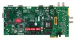


 工商网监
湘ICP备2023018690号
工商网监
湘ICP备2023018690号