Platform Manager Development Kit
User’s Guide
December 2010
Revision: EB58_01.2
�Platform Manager Development Kit
User’s Guide
Lattice Semiconductor
Introduction
Thank you for choosing the Platform Manager™ Development Kit. This user’s guide describes how to start using
the Platform Manager Development Kit, an easy-to-use system for evaluating and designing with the Platform Manager mixed-signal device. The kit serves as a development test environment to build designs for power supply management functions such as sequencing, power supply fault logging, trimming, reset generation, high-side MOSFET
drive and user logic I/O expansion in an FPGA.
Note: Static electricity can severely shorten the life span of electronic components. Use static-safe handling practices when using this development kit. Store the board in the supplied ESD safe bag. Handle all cables and interconnects in a static-safe environment.
Features
The Platform Manager Development Kit includes:
• Platform Manager Evaluation Board containing the Platform Manager LPTM10-12107 device in a 208-ball ftBGA
package
• USB programming support on-board
• 4Mbit SPI Flash memory for logging data and faults
• SPI and I2C interfaces
• 2x16 expansion header for I2C, SPI and general purpose data bus, I/O
• Two 4-bit DIP switches
• Three push-buttons for input control, reset, etc.
• DAC and A/D convertors for trimming power supplies
• LED displays
• LCD display
• Adjustable potentiometers for user faults or demos
• Thermistor circuit for temperature sensing
• LDO to demo sequencing and trim functions
• DC-DC convertor to demo sequencing and trim functions
• Two LDOs for main chip power and VCCIO supplies.
• VMON, voltage monitors for on-board and off-board power supply monitoring
• Off-board screw connectors for user loads and testing
• Prototyping/interface connections
• Pre-loaded Demo – The Platform Manager Development Kit contains a pre-loaded demo design that illustrates
many of the key features of the Platform Manager device.
• USB Connector Cable – The Platform Manager Evaluation Board is programmed via the USB cable driven from
the user’s computer. This USB cable is included in the Platform Manager Development Kit.
• Power Supply – The Platform Manager Evaluation board is powered by an AC adapter (included).
• Platform Manager Development Kit QuickSTART Guide – Provides information on connecting the Platform Manager Evaluation Board, getting started with the pre-programmed demo, and starting your own design.
• Platform Manager Development Kit Web Page – The Platform Manager Development Kit Web Page provides
access to the latest documentation, demo designs and additional resources.
2
�Platform Manager Development Kit
User’s Guide
Lattice Semiconductor
The contents of this user’s guide includes demo operation descriptions, top-level functionality descriptions of various portions of the evaluation board, descriptions of the on-board connectors, switches and a complete set of
schematics of the Platform Manager Evaluation Board.
Figure 1. Platform Manager Evaluation Board, Top Side
Slide Pot
R19
LEDs
D3-D6
D13, 15, 19-20
Slide Pot
R20
DIP SW2
JTAG Config.
Prototyping
Area
LCD
Display
Push-button
PB_B_SW2
5V Wall
Adapter
Plug
Push-button
PB_A_SW1
LEDs
D21-D24
JTAG
USB
Connect
SW10
1-4
SW9
1-4
Push- J8
J7
button LDO DC-DC
S1 2.5V
1.2V
Use the QuickSTART Guide First
Please use the Platform Manager Development Kit QuickSTART Guide that comes with the Platform Manager
Development Kit to get started. The QuickSTART Guide provides a “fast path” for working with the Platform Manager Evaluation Board and the pre-programmed Platform Manager demo. This user’s guide augments the QuickSTART guide by providing detailed descriptions of the board demos and schematic descriptions of the Platform
Manager Evaluation Board.
Platform Manager Device
The Platform Manager (LPTM10-12107) device is at the heart of the Platform Management Development Kit. This
device comes in a 208-ball ftBGA package and integrates both analog functions and digital functions, necessary for
advanced board and system level power control. It is a feature-rich device that allows for full power control and
reset generation or Platform Management.
Platform Manager is divided into a CPLD section and an FPGA section. The CPLD portion of the Platform Manager
is user-configurable logic that is tightly coupled to the power management analog signaling of the Platform Manager. The FPGA section allows for more expansive and sophisticated, LUT-based control of the Platform Manager
analog signaling as well as user-defined glue logic. See the Platform Manager Data Sheet for detailed information.
Analog features consist of 12 VMON analog voltage monitors with differential inputs for remote sense. Four highvoltage FET drivers are programmable for both slew rate and voltages up to 12V for driving high-side MOSFETs.
For trimming and margin control, the device uses A/D converters and D/A converters for closed loop trim, whereby
up to eight power supplies can be trimmed.
On the digital side, there are multiple internal clocks generated from an 8MHz internal oscillator and 16 open-drain
outputs. These are controlled by the CPLD section. The FPGA section contains 640 LUTs of FPGA logic and sup3
�Platform Manager Development Kit
User’s Guide
Lattice Semiconductor
ports flexible multiple voltage and I/O standard logic pins. The device is programmed with a JTAG interface and
runs off a 3.3V rail.
The FPGA section of the Platform Manager is optimized to meet the requirements of board management functions
including reset distribution, boundary scan management, fault logging, FPGA load control, and system bus interface. The FPGA section uses look-up tables (LUTs) and distributed memories for flexible and efficient logic implementation. This instant-on capability enables the Platform Manager devices to integrate control functions that are
required as soon as power is applied to the board.
Power management functions can be integrated into the CPLD and digital board management functions can be
integrated into the FPGA using the LogiBuilder tool provided by PAC-Designer® software. In addition, the FPGA
designs can also be implemented in VHDL or Verilog HDL through the ispLEVER® design tool.
The Platform Manager device supports a hardware I2C/SMBus slave interface that can be used to measure voltages through the Analog-to-Digital Converter or is used for trimming and margining using a microcontroller.
There are two JTAG ports integrated into the Platform Manager device: Power JTAG and FPGA JTAG. The Power
JTAG interface is used to program the power section of the Platform Manager and the FPGA JTAG is used to configure the FPGA portion of the device. The FPGA configuration memory can be changed in-system without interrupting the operation of the board management section. However, the Power Management section of the platform
Manager cannot be changed without interrupting the power management operation.
Figure 2. Device Block Diagram
LPTM10-12107
I2C
Analog Inputs
ADC
CPLD Logic
Margin/Trim
High-Voltage
Outputs
CPLD Inputs
CPLD Open-Drain
Outputs
CTimer
FPGA Logic I/O:
FTimer
Bank 0
Utility IP
Bank 1
Bank 2
FPGA Logic
Bank 3
4
�Platform Manager Development Kit
User’s Guide
Lattice Semiconductor
Demonstration Design
The Platform Manager Evaluation Board comes pre-programmed with the Platform Manager Demo to highlight the
power control and management abilities of the Platform Manager device. This demo performs the following functions:
• Drives LEDs to represent enable circuits for power supplies
• Reads various VMONs for board power
• Provides two slider pots to fire VMON trip points
• Sequences the LDO and Murata DC-DC power supply
• Receives inputs for switches and push-buttons
• Drives the LCD display panel
Components of this demo include:
• CPLD LEDs – There are four LEDs connected to CPLD outputs. LEDs light when open-drain outputs of the
CPLD are driven low. These are displayed to represent the board-level power supplies in the example or can be
used to show sequencing.
• FPGA LEDs – There are eight LEDs connected to FPGA output pins. LEDs light when the FPGA pins are driven
low. These are also sequenced to represent power supply enables and display different timing functions.
• Power Supplies – The board has two user-programmable power supplies that can be sequenced and trimmed
using the Platform Manager and PAC-Designer software. After the LEDs sequence for the three board power
supplies, the LDO and DC-DC converter are enabled.
• Slide Potentiometers – There are two slide potentiometers available to adjust VMON inputs for monitoring;
these are tied to VMON8 and VMON9. The slider pot input to VMON8 and VMON9 has a range of 0V to 3.3V.
The inputs can be set to trip on a window comparator within the Platform Manager. The two sliders are used in
the demo to start the sequence as well as to cause a fault to occur.
• LCD Display – The display is a 3-digit, standard 7-segment display and is driven from 24 FPGA output pins.
Segments are ON when each segment decode is driven in opposite polarity to the COM pin. The LCD is toggled
at approximately 60Hz using logic in the FPGA. The demo displays a hexadecimal value on the LCD, to change
the display, set the DIP switches.
• Hardware Power Supply Margin Function – The margining of the LDO and Murata DC-DC converter is done
with a signal from the push-buttons. There are two push-buttons adjacent to the DIP switches. Pressing
PBA_SW1 and PBB_SW2 drives the margin control to select between closed loop trim and margin settings.
Push-buttons are tied high with a pull-up to Bank2. Pressing PBB_SW2/PBA_SW1 drives a low on FPGA inputs.
The margining options shown in Table 1 are exercised in Step 5 of the demo.
Table 1. Margining Options
PBAB_SW2, PBA_SW1
Decoded in FPGA
LDO U11 2.5V
[High, High] 1,1 not pressed
Closed Loop Trim
2.5
1.2V
[High, Low] 1,0
Margin setting 1
2.375
1.14V
[Low, High] 0,1
Margin setting 2
2.625
1.26V
[Low, Low] 0,0
Margin setting 3
2.5V
1.2V
5
DC-DC Module 1.2V
�Platform Manager Development Kit
User’s Guide
Lattice Semiconductor
Initial Board Setup
• Set all DIP switches in SW9 and SW10 to the up/off position
• Set all DIP switches in SW2 to the on position
• Set slide pots R19 and R20 in the down position, toward the center of the board
• No jumpers should be installed
Step 1. Test Board Power, LED D1, and All Power Supplies
Step 1 shows the ability of the Platform Manager to monitor and sequence input power rails and on-board supplies.
There are five supplies connected to five separate VMON inputs on the Platform Manager Evaluation Board. The
first three supplies, 5V, 3.3V, and 2.5V, are power rails that the Platform Manager does not enable; it only monitors
them. The second 2.5V supply is an LDO that the Platform Manager enables and then monitors, and the 1.2V supply is a DC-DC converter that the Platform Manager enables and then monitors. There is also control from the Margin/Trim outputs on the Platform Manager to each of these supplies. Table 2 shows how the four LEDs in the
display follow the progress of the monitoring, enabling, and sequencing.
• Plug the 5V wall plug supply into the board supply plug.
• The blue LED D1 will be on and will remain lit while the board is powered.
• LEDs D21-D23 cycle through Steps 1-6 as shown in Table 2. Failure to cycle through the steps indicates a power
supply error.
Table 2. CPLD LED Pattern 1
Step
D24
D23
D22
D21
Function
1
off
off
off
ON
Wait for 5V supply good
2
off
off
ON
off
Wait for 3.3V supply good
3
off
off
ON
ON
Wait for 2.5V supply good
4
off
ON
off
off
Enable 2.5V LDO, wait for 2.5 good
5
off
ON
off
ON
Enable 1.2V LDO, wait for 1.2 good
6
off
ON
ON
off
Waiting for slide pots R19 and R20 to be
raised to top of slide
Step 2. Test Slide Pots R19-R20 and LEDs D3-D6, D13-D14, D19-D20 and D21-D24
Step 2 tests the position of the slide pots, and displays patterns and information on the LEDs and LCD display. The
slide pots are connected to two VMON inputs of the Platform Manager and are set to be “good” at about 3V. The
demo checks for both pots to be at good levels, then continues to the next step, which is to exercise various digital
outputs from the Platform Manager. Platform Manager outputs connect to the LEDs, as shown in the tables below,
and also to the LCD. The Closed Loop Trimming function for the LDO and DC-DC converter is also enabled at this
point.
• Move both slide pots R19 and R20 to the top (board edge) of their travel. LEDs D21-D24 will cycle on and off as
shown in Table 3.
Table 3. CPLD LED Pattern 2
State
D24
D23
D22
D21
1
off
ON
off
ON
2
ON
off
ON
Off
Back to
State 1
6
�Platform Manager Development Kit
User’s Guide
Lattice Semiconductor
• LEDs D3-D6, D13, D15 and D19-D20 will blink on and off in a binary sequence, with D13 the MSB and D3 the
LSB. The LCD will display “FF” in the right-most two digits.
• The voltage across the two pins of J8 will measure 2.5V +/- 1%.
• The voltage across the two pins of J7 will measure 1.2V +/- 1%.
Step 3. Test DIP Switches SW9 and SW10
Step 3 continues to exercise the digital inputs and outputs of the Platform Manager. Two of the DIP switches are
connected to the digital inputs of the Platform Manager. As these DIP switches are turned on or off, the LCD will
display two hexadecimal digits corresponding to the values produced by the four bits of each DIP switch.
• One by one, move DIP switches SW9-SW10 from the off/up position to the on/down position, and then back to
the off/up position. The LCD will display corresponding hexadecimal characters representing the hexadecimal
value of each DIP switch as it is moved. The value will change for each switch setting, as shown in Table 4. Other
values may be created by depressing more than one switch at a time.
Table 4. LCD - Hexadecimal Display
LCD
Display
SW10-1
SW10-2
SW10-3
SW10-4
SW9-1
SW9-2
SW9-3
SW9-4
FE
off
off
off
off
off
off
off
ON
Fd
off
off
off
off
off
off
ON
off
Fb
off
off
off
off
off
ON
off
off
F7
off
off
off
off
ON
off
off
off
EF
off
off
off
ON
off
off
off
off
dF
off
off
ON
off
off
off
off
off
bF
off
ON
off
off
off
off
off
off
7F
ON
off
off
off
off
off
off
off
Step 4. Test All Segments of the LCD Display
Similar to Step 3, Step 4 also uses digital inputs. In this step, one of the push-buttons which is connected to a digital input causes the LCD controller to display a looping sequence of numbers from 111-FFF. This sequence repeats
on the LCD as long as the push-button is depressed.
• Press and hold PB_B_SW2. The LCD display will show a counting sequence from a blank display, through 111,
222, 333 … FFF, and will repeat. The count may start anywhere in the sequence.
Step 5. Test Two Push-buttons and Trimming/Margining
This step shows the operation of the Closed Loop Trimming, and the ability of the Platform Manager to have different voltage profiles for margining which are selectable on the fly. There are three profiles used for this test. Profile 1
generates the target voltage (e.g., 1.2V) and adjusts the output voltage up by 5%. Profile 2 adjusts the output voltage down by 5%. Pressing either of the push-buttons shown below selects one of the profiles.
• Press and hold push-button PB_A_SW1.
– The voltage across the 2 pins of J8 will measure approximately 2.625V.
– The voltage across the 2 pins of J7 will measure approximately 1.26V.
• Release push-button PB_A_SW1.
• Press and hold push-button PB_B_SW2.
– The voltage across the 2 pins of J8 will measure approximately 2.375V.
– The voltage across the 2 pins of J7 will measure approximately 1.14V.
• Release push-button PB_B_SW2.
7
�Platform Manager Development Kit
User’s Guide
Lattice Semiconductor
Step 6. Test Push-button S1 for Reset Function
Step 6 illustrates the Platform Manager’s ability to sequence through a power-down scenario, and in this case,
restart the demo. When push-button S1 is depressed, the DC-DC converter is powered down, followed by the LDO.
The sequencer then returns to the beginning of the demo and starts over.
• Move slide pots R19-R20 to the down position (center of the board). Press and release push-button S1. The
board will reset and the test will start over.
VID Demo
The Platform Manager Evaluation Board is designed to demonstrate a form of Voltage control by Identification
(VID). This demo does not adhere to any specific “standard” VID specification. Rather, it demonstrates a generic
type of digital power supply control for the two power supplies on the Platform Manager Evaluation Board. In this
demo, the DIP switches are used to set the desired output voltage and to enable or disable the supplies. This demo
makes use of the Platform Manager Closed-loop Trim/Fault Logger IP core and a few lines of CPLD and FPGA
LogiBuilder code. This design demonstrates the following features:
• Implements closed loop trim on the 2.5V and 1.2V power supplies
• LEDs indicate the status of the LDO and Murata DC-DC power supply enables
• Receives inputs from switches and push-buttons
• A single VID lookup table can be shared between two different power supplies
• Closed-loop Trim/Fault Logger IP configuration
Note: the Fault Logger IP core is not enabled in this demo. For additional information about the Platform Manager
IP core, please refer to the Platform Management Utility Functions IP Core User’s Guide.
In order to experiment with the VID Demo, the Platform Manager device on the board must be reprogrammed with
the pre-compiled design file VID_Demo.jed.
Step 1. Download the VID Demo from the Lattice website.
The VID Demo can be downloaded from the Platform Manager Development Kit page of the Lattice Semiconductor
website.
Step 2. Program the Platform Manager with VID_Demo.jed
Connect the USB cable from the computer to the Platform Manager Evaluation Board.
Warning: If your operating system prompts you to install drivers for new hardware – do not install the
default USB drivers or you will have difficulty re-programming the Platform Manager device. Stop and
install the Lattice USB drivers found in the ispTools folder on your computer.
Open ispVM™ Version 17.9 or later. Scan the JTAG chain (F2) to find the LPTM10-12107 device. Double-click the
row to edit the device information. Browse to the VID_Demo.jed to open the file, set the Operation to Erase, Program, Verify and click OK. Click the GO button to start the re-programming. When the Platform Manager is programmed with the VID demo design LED D21 will be blinking on and off with a period of 500ms.
Step 3. Verify the 2.5V LDO VID Operation
Connect a Digital Volt Meter (DVM) to J8 to monitor the LDO output voltage. The voltage should be near zero with
LED D24 off after programming, power-up, or reset by momentarily pressing push button S1. Enter the VID setting
from Table 5 (SW[4:1]) on switch SW10 and momentarily press push-button PB_B_SW2 to enable the LDO and set
the trim target. Only the following VID codes are valid for the LDO: 0, 10, 11, 12, 13, 14, and 15. The VID code of
zero will disable the LDO and turn off LED D24. Any other VID will enable the LDO and turn on LED D24. VID table
entries 1 to 9 are below the LDO’s trim range and will result in an output near 2.38V. This is because the LDO’s trim
resistor network is designed to support a range of +/- 5% around the LDO’s nominal 2.5V output.
8
�Platform Manager Development Kit
User’s Guide
Lattice Semiconductor
Table 5. Common VID Code Lookup Table
VID
SW1
SW2
SW3
SW4
Voltage
VID Table
Code
0
0
0
0
0
0.00
0
1
1
0
0
0
1.14
570
2
0
1
0
0
1.16
580
3
1
1
0
0
1.18
590
4
0
0
1
0
1.19
595
5
1
0
1
0
1.20
600
6
0
1
1
0
1.21
605
7
1
1
1
0
1.22
610
8
0
0
0
1
1.24
620
9
1
0
0
1
1.26
630
10
0
1
0
1
2.40
1200
11
1
1
0
1
2.45
1225
12
0
0
1
1
2.50
1250
13
1
0
1
1
2.55
1275
14
0
1
1
1
2.60
1300
15
1
1
1
1
2.62
1310
Note: 0 = switch in the down position; 1 = switch in the up position.
Step 4. Verify the 1.2V Murata DC-DC Module VID Operation
Move the DVM to J7 to monitor the Murata DC-DC module output voltage. The measured voltage should be about
0.23V with LED D23 off after programming, power-up, or reset by momentarily pressing push button S1. Enter the
VID setting from Table 5 (SW[4:1]) on switch SW9 and momentarily press-push button PB_A_SW1 to enable the
DC-DC module and set the trim target. Only VID codes from 0 to 9 are valid for the DC-DC module. The VID code
of zero will disable the DC-DC module and turn off LED D23. Any other VID will enable the DC-DC module and turn
on LED D23. VID table entries 10 and above exceed the DC-DC module’s trim range and will result in an output
near 1.27V. This is because the trim resistor network is designed to support a range of +/- 5% around the DC-DC
module’s nominal 1.2V output. In Table 5, more VID codes are allocated to the DC-DC module to provide finer
adjustment of the lower voltage power supply. The VID Table Codes represent the closed loop trim ADC target
value and is generated from the IP configuration dialog.
Board Hardware Features
LED Outputs – CPLD
The Platform Manager Evaluation Board has four LEDs tied to the CPLD open-drain outputs. The LEDs are pulled
up to 3.3V and are lit when OUT6 through OUT9 are driven to a logic low.
9
�Platform Manager Development Kit
User’s Guide
Lattice Semiconductor
Figure 3. CPLD LEDs
+3.3V
R120
2.2k
R121
2.2k
DI
SM/R_0603
DI
SM/R_0603
D21
R123
2.2k
DI
SM/R_0603
DI
SM/R_0603
D24
RED
DI
D23
RED
DI
D22
RED
DI
RED
DI
R122
2.2k
OUT6
OUT7
OUT8
OUT9
LED Outputs – FPGA
The eight FPGA LEDs are tied to Bank0 of the FPGA pins. They are pulled up to 3.3V and the LEDs are lit when
the outputs are driven with a logic low.
Figure 4. FPGA LEDs
+3.3V
+3.3V
5
10
RN2E
RN2F
RN2G
RN2H
RN2A
RN2B
RN2C
2.2k
DI
2.2k
DI
2.2k
DI
2.2k
DI
2.2k
DI
2.2k
DI
2.2k
DI
6
7
9
8
2
1
RN2D
2.2k
DI
4
3
D13
D15
D19
D20
RED
DI
RED
DI
RED
DI
RED
DI
FPGA PIN
B3
F_LED7
B2
F_LED6
B1
F_LED5
A3
F_LED4
C4
F_LED3
C3
F_LED2
C2
F_LED1
B4
F_LED0
+3.3V
+3.3V
5
10
RN1E
RN1F
RN1G
RN1H
RN1A
RN1B
RN1C
RN1D
2.2k
DI
2.2k
DI
2.2k
DI
2.2k
DI
2.2k
DI
2.2k
DI
2.2k
DI
2.2k
DI
7
6
D6
RED
DI
8
9
2
1
D4
RED
DI
D5
RED
DI
3
4
D3
RED
DI
Open-Drain CPLD Outputs
There are 16 available outputs for the CPLD. These include four HVOUT pins and 12 3.3V open-drain outputs. The
outputs are set up to drive four LEDs for the CPLD, four Fault Logging outputs or general purpose signals to the
FPGA, SMBUS Alert and the OUT16_Timer signal. OUT11 and OUT12 are used for enables to the user supplies.
OUT16_Timer drives an FPGA clock input for slow clocks and long timers in the FPGA. OUT16 time base is calculated automatically in PAC-Designer and depends on the time delay chosen by the user in the FTimer blocks.
10
�Platform Manager Development Kit
User’s Guide
Lattice Semiconductor
Figure 5. Open-Drain CPLD Outputs
+3.3V
+3.3V
R72
R75 R83 R84 R87 R88 R71 R89 R91
R92 R90
R174
SM/R_0603
DI
1k
SMBUS ALERT
LED CPLD
LED CPLD
LED CPLD
LED CPLD
4.7k 4.7k 4.7k 4.7k 4.7k 4.7k 4.7k 4.7k 4.7k 4.7k 4.7k
DI
DI DI DI DI DI DI DI DI
U70H
DI DI
G13
T10
R10
T11
T12
R11
R12
P10
T13
P11
T14
R13
SMBA_OUT5
OUT6
OUT7
OUT8
OUT9
OUT10_FAULT
OUT11
OUT12
TO PROTO, ENABLE LDO, FPGA I/O=T2
TO PROTO, DC/DC ENABLE, FPGA I/O=T3
OUT13_STAT2
OUT14_STAT1
OUT15_STAT0
OUT16_TIMER
SMBA_OUT5
OUT6
OUT7
OUT8
OUT9
OUT10
OUT11
OUT12
OUT13
OUT14
OUT15
OUT16
OUT16 DRIVES TIMERS FOR FPGA
DRIVES R9 FPGA pin,1K PULL UP, FOR FTIMERS
LPTM_208BGA
DIGITAL OPEN DRAIN CPLD OUTPUTS
I/O Expansion Header
The Platform Manager Evaluation Board has an unpopulated 32 pin-header for access to I/O signals for the FPGA.
These connections are labeled on the board. This allows users to develop custom designs and expand the I/O
count for the board
Figure 6. I/O Expansion Header
+3.3V
+3.3V
J15
+3.3V
HEADER_D8
HEADER_D9
HEADER_D10
HEADER_D11
HEADER_D12
HEADER_D13
HEADER_D14
HEADER_D15
SMBA_OUT5
SCP_SDA
SCP_SCL
A2D_IN
R15
4.7k
1
3
5
7
9
11
13
15
17
19
21
23
25
27
29
31
2
4
6
8
10
12
14
16
18
20
22
24
26
28
30
32
DNI
HEADER_D0
HEADER_D1
HEADER_D2
HEADER_D3
FLT_BUSY
FLT_FULL
FLT_CLEAR
FLT_READY
SYS_SPI_SS
SYS_SPI_SCLK
SYS_SPI_MISO
SYS_SPI_MOSI
A2D_OUT
D0
D1
D2
D3
BUSY
FULL
CLR
RDY
N/C
SS
SCLK
MISO
MOSI
GND
ADO
SILKSCREEN NAMES
SILKSCREEN NAMES
D8
D9
D10
D11
D12
D13
D14
D15
SMBA
SSDA
SSCL
N/C
N/C
GND
ADI
R14
4.7k
The interface has generic I/Os, SPI control signals, I2C control and fault logging signals. All of these can be set up
and programmed by the user for custom I/Os.
11
�Platform Manager Development Kit
User’s Guide
Lattice Semiconductor
LCD Display
The LCD provided is driven by FPGA outputs. The LCD is a set of three 7-segment displays. For more information
on LCD usage, see the description of the Platform Manager Demo earlier in this document.
Figure 7. LCD Display
LCD NO BACKLIGHT: DRIVE WITH FPGA OUTPUTS WITH PHASE CONTROL TO LIGHT SEGMENTS
Part#
LCD-S301C31TR
U14
1
COM
G1
24
2
E1
F1
23
3
D1
A1
22
4
C1
B1
21
5
DP1
G2
20
6
E2
F2
19
7
D2
A2
18
8
C2
B2
17
9
DP2
G3
16
10
E3
F3
15
11
D3
A3
14
12
C3
B3
13
LUMEX-LCD1
BANK3
PCB Footprint = LUMEX301
DI
SYS_SPI_MISO
SYS_SPI_SS
PL10B
PL10D
PL10A
PL11D
PL9D
PL11C
PL9C
PL8C
PL11B
PL8D
PL8A
PL11A
PL6A
PL5D
PL7D
PL7B
PL6D
PL5C
PL5B
PL7A
PL4D
PL5A
PL3D
PL3B
PL4A
PL3A
PL2B
PL2A
R1
P2
P1
N3
N2
M3
M2
M1
L3
L2
L1
K3
K2
K1
J4
J3
J2
J1
H4
H3
H2
G4
G3
G2
G1
F3
F2
F1
SYS_SPI_SCLK
SYS_SPI_MOSI
BANK 3
U70D
LPTM_208BGA
VCCIO3 BANK3= 3.3V
12
�Platform Manager Development Kit
User’s Guide
Lattice Semiconductor
DIP Switches
The Platform Manager Evaluation Board.provides eight DIP switches that are connected to the FPGA portion of the
Platform Manager device. In addition, there are four DIP switches for JTAG configuration (SW2).
Figure 8. DIP Switches
A_SW1
A_SW2
A_SW3
A_SW4
B_SW1
B_SW2
B_SW3
B_SW4
+2.5V
A_SW1
A_SW2
A_SW3
A_SW4
B_SW1
B_SW2
B_SW3
B_SW4
+2.5V
R98
DI
+2.5V
R94
DI
SM/R_0603
100k
R93
DI 100k
R100
DI 100k
R96
DI 100k
R99
DI
R95
DI
100k
4
3
2
1
4
3
2
1
100k
SW10
SWDIP-4
DI
SW9
SWDIP-4
DI
CT1934MS-ND
5
6
7
8
5
6
7
8
SM/R_0603
100k
R97
DI 100k
B_SW
+2.5V
+2.5V
R80
10k
DI
SM/R_0603
R79
10k
DI
SM/R_0603
PB_B_SW
PB_B_SW2
4
C49
0.1uF
DI
CT1934MS-ND
A_SW
PB_A_SW
PB_A_SW1
1
C50
0.1uF
DI
3
2
4
1
3
2
DI
PCB Footprint = SMT_SW
DI
PCB Footprint = SMT_SW
Part Number:EVQ Q2K03W
Part Number:EVQ Q2K03W
13
�Platform Manager Development Kit
User’s Guide
Lattice Semiconductor
VMON Slide Potentiometers
The two potentiometers are tied to VMON8 and VMON9; these can be used to simulate a fault or to trip a comparator to turn on or off a display or power supply. The voltage on the potentiometer can also be read out from the A/D
converter using the I2C port.
Figure 9. VMON Slide Potentiometers
VOLTAGE MEASUREMENT
+3.3V
3
R19
1k
DI
R85 1k DI
2
1
SLIDER POT-VM9
VMON9P
VMON8P
VOLTAGE MEASUREMENT
+3.3V
3
R20
1k
DI
2
1
R86 1k DI
SLIDER POT-VM8
SM/R_0603
HVOUT MOSFET Ramp Circuits
HVOUTs are used for driving N-channel MOSFETs. HVOUT1 and HVOUT2 are tied to MOSFETs mounted on the
evaluation board. Each HVOUT can be set for a different drive current to show voltage ramps at the source of the
FET. Note that HVOUT1 can be monitored on VMON1P and HVOUT2 can be monitored on VMON2.
HVOUT3 and HVOUT4 are routed to the prototype area for off-board use.
14
�Platform Manager Development Kit
User’s Guide
Lattice Semiconductor
Figure 10. HVOUT MOSFET Ramp Circuits
+3.3V
C81
1uF
DI
SM/C_0603
HVOUT4 HVOUT3,HVOUT4 GO TO PROTO
3
HVOUT3
R204
HVOUT2
2
SM/R_0603
U70I
HVOUT4
HVOUT3
HVOUT2
HVOUT1
Q6
2N7002E
DI
1
1k
DI
VMON11P
C79
1uF
DI
SM/C_0603
K13
L13
E13
F13
R186
200
DI
SM/R_0603
+3.3V
C82
1uF
DI
SM/C_0603
3
LPTM_208BGA
R205
HVOUT1
SM/R_0603
1k
DI
C80
1uF
DI
SM/C_0603
2
1
Q7
2N7002E
DI
VMON12P
R187
200
DI
SM/R_0603
HVOUT1,HVOUT2 drivers do not sequence on board power, they
demonstrate a ramp circuit, controlled by PAC Designer
settings and visible on a scope. FETS are 250mA max!
VMON Voltage Monitor Inputs
There are 12 VMON inputs to the analog section of the device. These are routed to board power supplies, user
power supplies, the temperature sensing circuits, slider pots and the prototype area. All VMONs voltages can be
read out from the A/D converter using I2C. The VMONs are described in Table 6.
Table 6. VMON Descriptions
VMON
Description
VMON1
Tied to the prototype area for off-board monitoring or trim applications.
VMON2
Tied to the prototype area for off-board monitoring or trim applications.
VMON3
Monitor for 2.5V power supply used on FPGA Bank1 VCCIO.
VMON4
Monitor for 5V power supply, main wall adapter rail.
VMON5
Voltage monitor for the user DC-DC module supply.
VMON6
Voltage monitor for the user LDO supply.
VMON7
Temperature monitor on the thermistor circuit.
VMON8
Voltage monitor on slide pot R20.
VMON9
Voltage monitor on slide pot R19.
VMON10
Monitor for main 3.3V rail.
VMON11
Voltage monitor for FET ramp circuit and Q6 MOSFET.
VMON12
Voltage monitor for FET ramp circuit and Q7 MOSFET.
15
�Platform Manager Development Kit
User’s Guide
Lattice Semiconductor
Figure 11. Voltage Monitor Inputs
U70K
FET RAMP Q7
VMON12P
FET RAMP Q6
VMON11P
D15
D16
E15
E16
F15
F16
G15
G16
H15
H16
J15
J16
K15
K16
L15
L16
M15
M16
N15
N16
P15
P16
R15
R16
+3.3V
VMON9P
VMON8P
TO THERMISTOR
TEMP1P
VOUT_LDOM
VOUT_LDOP
VOUT_MODULEM
VOUT_MODULEP
+5V
VMON2P VMON2M TO PROTO
+2.5V
VMON2M
VMON2P
VMON1M
VMON1P
VMON12M
VMON12P
VMON11M
VMON11P
VMON10M
VMON10P
VMON9M
VMON9P
VMON8M
VMON8P
VMON7M
VMON7P
VMON6M
VMON6P
VMON5M
VMON5P
VMON4M
VMON4P
VMON3M
VMON3P
VMON2M
VMON2P
VMON1M
VMON1P
LPTM_208BGA
Trim DACs
The Trim DACs are used for margining and trimming power supplies. On the Platform Manager Evaluation Board,
the LDO is hooked to TRIM6 and VMON6P/VMON6M. The Murata DC-DC Module is hooked to TRIM5 and
VMON5P/VMON5M. These resources provide for closed loop trimming of the supply.
The demo design is set up to trim the LDO to 2.5V and the DC-DC module to 1.2V. Each supply has been biased
on the board with resistors for setting the output voltage as well as the resistors required for trimming. If the user
would like to select different values, the resistors in the trim network must be changed.
Figure 12. Trim DACs
TRIM DACS
U70L
TRIM8
TRIM7
TRIM6
TRIM5
TRIM4
TRIM3
TRIM2
TRIM1
C16
C15
C14
B16
B15
B14
A15
A14
TRIM6PIN
TRIM5PIN
R64
DI SM/R_0603
TO LDO
TRIM6_LDO
100
C67
.1uF
DI SM/C_0603
TRIM1PIN
LPTM_208BGA
TRIM DACS
R66
DI SM/R_0603
TO MODULE
TRIM5_MODULE
100
C68
.1uF
DI SM/C_0603
R129
DI SM/R_0603
TO PROTO
TRIM1
100
C87
.1uF
DI SM/C_0603
ADDED TRIM1 FOR EXTERNAL
USE TO PROTO. USE
VMON1P,VMON1M WITH TRIM1
Trimming User Supplies: LDO 2.5V
The trim circuit and LDO user power supply is set up on the board to output 2.5V to the load connectors. Note that
in its default configuration, there is a relatively light power load on the evaluation board. Users may add additional
16
�Platform Manager Development Kit
User’s Guide
Lattice Semiconductor
loads to the green screw connectors located at J8. The load should not exceed the maximum ICC of the LDO
(1.2A).
Figure 13. LDO 2.5V
WALL ADAPTER
.05
DI
SM/R_2512
5VRAW
DIODES INC
Part Number AP7168-SPG-13
1.2AMP LDO WITH ENABLE
AND TRIM CAPABILITIES:
5VRAW
SM/R_0603
R115
10k
DI
DI
C44
DI
C53
1uF
.1uF
SM/C_0603
SM/C_0603
1
2
3
4
SM/C_0603 SM/C_0603
C51
SM/R_0603
R18
100k
U11 DI
DI
R17
10k
DI
SM/R_0603
R61
VMON6P (K16)
U11_OUT
FROM
.1uF
DI
IN
POK
NC
EN
OUT
FB
NC
GND
U11_OUT
C52
10uF
DI
8
7
6
5
DI
C59
R69
21.5k
DI
SM/R_0603
R116
1k
DI
1uF
tantalum
LDO_TRIM
SM/C_0603
R76
10k
DI
SM/R_0603
AP7168
SOP-8L-EP PACKAGE
DIODES INC
SM/R_0603
Q4
2N3904
DI SM/SC70_213
ROUTE TRACE TO
CONNECTOR FOR
SENSE LINE
R130
OUT11
SM/R_0603
SM/R_0603
R36
4.7k
DNI
R39
4.7k
DNI
R38
TRIM6_LDO
46.4k DI
TRIM LDO
DI
VOUT_LDOP
SM/R_0402
VOUT_LDO
1
LDO_TRIM
TO TRIM PIN,VREF LDO
R40
4.7k
DNI
SM/R_0603
VOUT NOM=2.5V
B
Rseries
R37
4.7k
DNI
SM/R_0603
A
ENABLE LDO
ROUTE TRACE TO
CONNECTOR FOR
SENSE LINE
0
VOUT_LDOM
J8
277-1947-ND DIGIKEY
2 Position Terminal Block
PLACE RESISTORS IN 'H' CONFIGURATION AND
LEAVE ENOUGH ROOM FOR END USER TO SOLDER
KEEP RESISTORS CLOSE TO LDO
17
�Platform Manager Development Kit
User’s Guide
Lattice Semiconductor
Trimming DC-DC Module
The DC-DC Module (Murata OKR DC-DC Module 1.2V) is set to VOUT=1.2V. The trim network is shown connected to TRIM5_Module in Figure 14. If the user needs to program the supply at a different voltage, the resistors
R110, R111, R109, R106 will need to be changed and a new DC-DC macro built within PAC-Designer.
Figure 14. DC-DC Module
FROM
WALL ADAPTER
3,6,10 AMP MODULE WITH ENABLE
AND TRIM CAPABILITIES:
MURATA OKR DC/DC MODULE
5VRAW
6AMP
DC/DC MOD
OKR-T
U71 DI
R63
U71_OUT
REMOTE
VIN
GND
VOUT
TRIM
MURATA SIP
SM/R_0603
R113
10k
DI
SM/R_0603
1
2
3
4
5
R114
10k
DI
.01
DI
SM/R_2512
VREF=.591
U71_OUT
TO VMON5 TO MEASURE
VREF_MODULE
tantalum
DI
C55
DI
C57
.1uF
1uF
DI
C58
.1uF
DI
R112
1k
1uF
Tantalum
SM/C_0603
SM/C_0603 SM/C_0603
R110
4.32k
DI
R109
100k
DNI
R107
TRIM5_MODULE
TO TRIM PIN,VREF
R_PUP DAC
SM/C_0603 SM/R_0603
ROUTE TRACE TO
CONNECTOR FOR
SENSE LINE
R131
DI
9.09k DI
VOUT_MODULEP
SM/R_0402
1
R108
1.69k
DI
VOUT_MODULE
R_PDN_SUPPLY
PLACE RESISTORS IN 'H' CONFIGURATION AND
LEAVE ENOUGH ROOM FOR END USER TO SOLDER
KEEP RESISTORS CLOSE TO MODULE
DC/DC MODULE
R_SERIES
R111
100k
DNI
ROUTE TRACE TO
CONNECTOR FOR
SENSE LINE
0
VOUT_MODULEM
B
tantalum DI
C54
SM/C_0805
10uF
DI
C56
A
ENABLE MODULE
Q2
2N3904
DI SM/SC70_213
J7
277-1947-ND DIGIKEY
2 Position Terminal Block
Temperature Monitoring
The board has a thermistor mounted as a voltage divider circuit that is routed to VMON7. This analog input is a
standard VMON. The VMONs are used as a programmable comparator, each has two programmable trip points.
By setting the trip points in the software, an over-temp can be used to shut down a power supply or light an LED
when a certain temperature is read. The VMON can also be set to a window comparator with a high and low trip
point. The VMONs can be read out from the A/D converter using I2C.
Figure 15. Temperature Monitoring
+3.3V
TEMPERATURE MEASUREMENT
+3.3V
R62 DI
1K
SM/R_0402
TEMP1P
TO VMON7P
R60 DI
1k
SM/R_0402
THERM:ERTJ0ET102J: 1k 402 size
18
�Platform Manager Development Kit
User’s Guide
Lattice Semiconductor
RESET
The evaluation board has one reset push-button. This signal is routed to IN2 of the CPLD. Equations can be written
in PAC-Designer for resetting the CPLD sequence. The reset is also routed to the FPGA, where it drives pin F4.
Equations must be written to use these pins as a reset function. It is not a full board or chip reset unless the
designer sets it up that way.
Figure 16. Reset
+3.3V
+3.3V
SM/R_0603
R78
10k
DI
RESET_ALL
RESET_ALL
RESET_ALL
4
RESET FOR FPGA=GENERIC_INPUT
RESET FOR CPLD_POWR=IN2
S1
1
RESET_ALL
C47
0.1uF
DI
SM/C_0603
3
2
DI
PCB Footprint = SMT_SW
Part Number:EVQ Q2K03W
Panasonic SMD
On-board SPI Flash Memory
The Platform Manager Evaluation Board has a 4MBit SPI Flash memory that is used to record faults in the system.
Fault logging is accomplished by monitoring the VMON pins and activating an output pin when a power supply falls
outside its programmed range. The VMONs have programmable trip points and support a window compare. If the
voltage falls outside the window, a fault is triggered. When a fault is triggered, output pins from the CPLD write to
the FPGA and are decoded to represent different fault conditions. Once the fault has occurred, the FPGA finds the
next available memory page and writes out the data using SPI. The stored data is non-volatile. The board can be
powered down and data read back out of the Flash using design utilities. Lattice provides software tools, reference
designs and IP cores that work with the Platform Manager Development Kit or designers can use their own
designs.
Figure 17. On-Board SPI Flash Memory
4MBIT SPI FLASH MEMORY TO STORE FAULT LOGS CONNECTED TO FPGA
PINS: 2 FOOTPRINT OPTION, POPULATE ONLY ONE
8-SOIC PACKAGE DI
+3.3V
8-UDFN PACKAGE DNI
+3.3V
4MBit SPI
4MBit SPI
U73
U69
C22
0_1uF
DI
SM/C_0603
8
7
3
4
Vcc
Reset
W
Vss
1
6
5
2
S
C
D
Q
MEM_SPI_SS
MEM_SPI_SCLK
MEM_SPI_MOSI
MEM_SPI_MISO
C2
0_1uF
DI
SM/C_0603
AT25DF041A
Atmel AT25DF041A-SH-B =
8
7
3
4
Vcc
Reset
W
Vss
S
C
D
Q
1
6
5
2
AT25DF041A
Atmel AT25DF041 =
(SOIC type)
19
MEM_SPI_SS
MEM_SPI_SCLK
MEM_SPI_MOSI
MEM_SPI_MISO
(8-UDFN type)
�Platform Manager Development Kit
User’s Guide
Lattice Semiconductor
Clock Routing
Table 7. Pin Interconnection for Timers
Package
OUT16 Timer4
Route to
Bank
208-ball ftBGA
OUT16 (R13)
PB9C (R9)
Bank2
To set up additional logic and sequencers in the FPGA in PAC-Designer, the 250kHz CPLDCLK is driven externally
and routed to an FPGA pin for a 250kHz clock input. Table 8 shows the connections required for the CPLDCLK,
which is externally connected between the dedicated CPLDCLK output pin and an FPGA input pin.
Table 8. Pin Interconnection for CPLDCLK
Package
CPLDCLK
Route to
Bank
208-ball ftBGA
CPLDCLK (C11)
PT6B (D5)
Bank0
Table 9. Pin Interconnection for MCLK
Package
MCLK
Route to
Bank
208-ball ftBGA
MCLK (B11)
PT5B (A2)
Bank0
The 8MHz internal MCLK is also connected externally to the FPGA from the 8MHz MCLK output to an FPGA input.
This clock is used for communication and I/O as well as an internal main fabric clock. The Master mode is used to
enable the 8MHz internal oscillator.
Figure 18. Clock and Timer Dialog Box
Clock Routing at the Pin
When the design is compiled, PAC-Designer processes the sequencers and synthesizes the logic to be run
through fitting and JEDEC generation. These steps are taken care of automatically, once initiated. A report file and
a Verilog file are saved in the directory tree structure.
Routing
When using the FPGA clocks and timers, it is important to understand the routing of the pins and the clocks
required. In PAC-Designer software, the 8MHz internal clock must be set up for driving to the outside pins and connected externally from pin to pin. The 250kHz PLDCLK is also used externally.
20
�Platform Manager Development Kit
User’s Guide
Lattice Semiconductor
Figure 19. External Connections for Clocks
3.3V
1K 1K
1K
OUT16 R13
CPLDCLK C11
MCLK B11
FTimer
FPGA Logic
PB9C
PT6B
PT5B
To FTimer
250kHz
8MHz
R9
D5
A2
External Connections for 208-Ball ftBGA
CPLD Logic and CLK Outputs
Ordering Information
Description
Ordering Part Number
Platform Manager Development Kit
China RoHS Environment-Friendly
Use Period (EFUP)
LPTM10-12107-DEV-EVN
Technical Support Assistance
Hotline: 1-800-LATTICE (North America)
+1-503-268-8001 (Outside North America)
e-mail: techsupport@latticesemi.com
Internet: www.latticesemi.com
Revision History
Date
Version
Change Summary
October 2010
01.0
Initial release.
October 2010
01.1
Added Appendix C, Configuring the ispMACH 4000 Mux for the Platform
Manager Development Kit.
December 2010
01.2
Added VID Demo text section.
© 2010 Lattice Semiconductor Corp. All Lattice trademarks, registered trademarks, patents, and disclaimers are as
listed at www.latticesemi.com/legal. All other brand or product names are trademarks or registered trademarks of
their respective holders. The specifications and information herein are subject to change without notice.
21
�22
A
B
C
USB_TDO
USB_TCK
USB_TMS
HEADER 3
SPI
I2C
010
111
110
101
100
011
JTAG
MODE
001
5
HEADER 3
000
JTAG_SEL
J16
DI
J14
DI
J12
DNI
HEADER 3
1
2
3
1
2
3
1
2
3
1
2
3
USB_TDI
HEADER 3
4KJ_TDO
4KIO_TDO
4KJ_TCK
4KIO_TCK
4KJ_TMS
4KIO_TMS
4KJ_TDI
4KIO_TDI
8 HEADER
1
2
3
4
5
6
7
8
4KIO_TCK
+3.3V
4KIO_TDO
4KIO_TDI
N/C
PLUG
4KIO_TMS
DI
SW2C
SW_SPST_4
4
DI
3
JTAG_SEL_0
JTAG_SEL_1
JTAG_SEL_2
3
SW2D
SW_SPST_4
USB_GPIO_H0
USB_GPIO_H1
USB_GPIO_L0
USB_GPIO_L1
USB_GPIO_L2
USB_GPIO_L3
Optional JTAG header for straight through 1x8 no USB
DNI
J1
R222
330
DI
SW2B
SW_SPST_4
USB_6MHZ
DI
+3.3V
DI
SM/LED_0603
D12
Red
7
2
J11
DNI
6
3
4KIO_TCK
4KIO_TMS
4KIO_TDI
4KIO_TDO
U2
DI
2
BANK0_0
BANK0_1
BANK0_2
BANK0_3
BANK0_4
BANK0_5
BANK0_6
BANK0_7
LC4032/4064-T44
BANK0_8
BANK0_9
BANK0_10
BANK0_11
BANK0_12
BANK0_13
GOE0/BANK0_14
CLK0/I
U2
2
+3.3V
4KJ_TDI
4KJ_TDO
4KJ_TMS
4KJ_TCK
Lattice Number:LC4064V-5TN44C
2
3
4
7
8
9
13
14
15
16
41
42
43
44
40
39
+3.3V
11
33
VCC
VCC
Date:
Size
B
0
Aug23 2010
SCP_SDA
SCP_SCL
SYS_SPI_SCLK
SYS_SPI_MOSI
SYS_SPI_SS
SYS_SPI_MISO
C69
0.1uF
DI
SM/C_0603
1
R2
4.7K
DI
1
Sheet
C
C
Schematic Rev
R1
4.7K
DI
Board Rev
1
of 15
+3.3V
+3.3V
SM/C_0603
+3.3V
FLT_READY
FLT_CLEAR
FLT_FULL
FLT_BUSY
C71
0.1uF
DI
Lattice Semiconductor Applications
Email: techsupport@Latticesemi.com
Phone (503) 268-8001 -or- (800) LATTICE
PM_TCK
PM_TMS
PM_TDI
PM_TDO
C65
0.1uF
DI
SM/C_0603
Project
LPTM10-12107-DEV-EVN
Title
A_MUX
SW_SPST_4
SW2A
18
19
20
21
22
24
25
26
29
30
31
35
36
37
38
17
DI
SM/C_0603
C64
0.1uF
DI
BANK1_0
BANK1_1
BANK1_2
BANK1_3
BANK1_4
BANK1_5
BANK1_6
BANK1_7
BANK1_8
BANK1_9
BANK1_10
BANK1_11
BANK1_12
BANK1_13
GOE1/BANK1_14
CLK2/I
GND
GND
GND
GND
5
12
27
34
4
5
4
28
6
VCCO1
VCCO0
TDI
TDO
TMS
TCK
1
32
23
10
FTDI USB to
MULTIPLE JTAG Interface
Sheet
8
1
D
5
A
B
C
D
Lattice Semiconductor
Platform Manager Development Kit
User’s Guide
Appendix A. Schematic
Figure 20. Mux
�23
A
B
C
D
CLOCK PINS
C48
0.1uF
DNI
SM/C_0603
0
R106
SM/R_0603 10k
DNI
+3.3V
SM/R_0603
DI
R117
1k
MCLK
CPLDCLK
A2
A3
B1
B2
B3
B4
C2
C3
C4
C5
D1
D2
D3
D4
D5
D6
E1
E2
E3
E4
F4
BANK0 IS 3.3V
BANK0
LPTM_208BGA
PT5B
PT7E
PT4E
PT5A
PT7A
PT8A
PT4C
PT4B
PT6C
PT9E
PT3F
PT3E
PT3C
PT6A
PT6B
PT9A
PT3B
PT2F
PT2C
PT2E
PT2B
U70A
5
RESETB
SDA_CPLD
SCL_CPLD
SM/R_0603
SM/R_0603
DI
DI
R101
R118
1k
1k
+3.3V
A12
B12
B11
C11
C12
CREF
VCOM
0
PUSH-BUTTON
B_SW1
B_SW2
B_SW3
B_SW4
PB_B_SW
A_SW1
A_SW2
A_SW3
A_SW4
PB_A_SW
H14 CREF
J14 VCOM
J25
B2S
4
J26:TEST HOLES, .038 SIZE, .100MIL
APART: SILK = RESETb-CPLD AND PIN1= GND
J26
B2S
A_SW1
A_SW2
A_SW3
A_SW4
B_SW1
B_SW2
B_SW3
B_SW4
J25:TEST HOLES, .038 SIZE, .100MIL
APART:SILK= CREF AND PIN1=VCOM
I2C clks, RESETB, from CPLD
LPTM_208BGA
SDA
SCL
MCLK
CPLDCLK
RESETB
U70M
SM/R_0603
DI
R103
1k
+3.3V +3.3V
FPGA GOES TO BALL PT2B F4 BALL ON BANK0 (3.3V)
FOR CPLD GOES TO BALL C10, DIGITAL IN2 3.3V
RESET_ALL
+3.3V +3.3V
RESET_ALL
RESET_ALL
SCP_SDA
SCP_SCL
F_LED4
F_LED5
F_LED6
F_LED7
F_LED0
F_LED1
F_LED2
F_LED3
MEM_SPI_SS
MEM_SPI_SCLK
MEM_SPI_MOSI
MEM_SPI_MISO
CPLDCLK
SMBA_OUT5
SDA_CPLD
SCL_CPLD
SPI FAULTS TO
SPI FLASH
FROM CPLD TO FPGA
FROM CPLD TO FPGA
FROM CPLD TO FPGA
MCLK
DIP-B
DIP-A
FROM CPLD 8MHZ
4
BANK1
LPTM_208BGA
PR3D
PR6D
PR9B
PR3B
PR2D
PR6C
PR8C
PR10A
PR2B
PR4D
PR8A
PR10C
PR11C
PR4B
PR7B
PR11A
U70B
BANK1=2.5V FIXED LDO
A5
A7
A9
B5
B6
B7
B8
B9
C6
C7
C8
C9
D10
D7
D8
D9
TP1
DI
R102
10k
+3.3V
FLT_READY
OUT14_STAT1
FLT_CLEAR
FLT_FULL
FLT_BUSY
TP for SLEEPN
SLEEPN
OUT10_FAULT
3
2 CPLD INPUTS connected to FPGA.
FOR LONG TIMERS: OUT16 drives R9
TO PROTO,LDO ENABLE , FPGA I/O=T2
TO PROTO, DC/DC ENABLE, FPGA I/O= T3
3
1
5
2
HEADER_D3
HEADER_D2
HEADER_D1
HEADER_D0
OUT16_TIMER
OUT11
OUT12
IN3
IN4
OUT15_STAT0
OUT13_STAT2
HEADER_D12
HEADER_D11
HEADER_D10
HEADER_D9
HEADER_D8
HEADER_D15
HEADER_D14
HEADER_D13
2
Date:
Size
B
Aug 23 2010
Project
LPTM10-12107-DEV-EVN
Title
BANK0_BANK3
1
Sheet
Lattice Semiconductor Applications
Email: techsupport@Latticesemi.com
Phone (503) 268-8001 -or- (800) LATTICE
C
C
Schematic Rev
Board Rev
2
of 15
SEE LCD PAGE FOR I/O
PL10B
BANK3 MARKER
LPTM_208BGA
PL2A
U70D
BANK2=3.3V LDO
PB9F
PB5D
PB7C
PB8C
PB9E
PB3B
PB3D
PB5B
PB5C
PB7E
PB8D
PB9D
PB2A
PB3C
PB4A
PB4F
PB6B
PB7B
PB8A
PB9C
PB2C
PB2D
PB4D
PB6C
PB7A
PB9A
U70C
1
BANK2
LPTM_208BGA
N10
N6
N7
N8
N9
P3
P4
P5
P6
P7
P8
P9
R2
R3
R4
R5
R6
R7
R8
R9
T2
T3
T5
T6
T7
T9
2
BANK2 MUST RUN ON 3.3V FOR JTAG
1
LCD CONTROL LINES
2
BANK3 USED FOR
1
A
B
C
D
Lattice Semiconductor
Platform Manager Development Kit
User’s Guide
Figure 21. Bank0, Bank3
�24
A
B
C
+3.3V
5
C66
DI 0.1uF
SM/C_0402
+3.3V
U11_OUT
RAIL1=LDO
DNI
3
V+
2
GND
INA197
VIN+
U13 4
5
1
OUT
VINTP6
V1_ICC
VOUT_LDOP
1
D
4
4
3
+3.3V
3
DNI
3
V+
2
GND
INA197
VIN+
U15 4
SM/C_0402
C70
DI 0.1uF
+3.3V
U71_OUT
1
OUT
VIN-
5
2
2
VOUT_MODULEP
TP8
V2_ICC
RAIL1=DC/DC MODULE
1
5
Date:
Size
B
Aug 23 2010
Project
LPTM10-12107-DEV-EVN
Title
CURRENT_SENSE
1
Sheet
Lattice Semiconductor Applications
Email: techsupport@Latticesemi.com
Phone (503) 268-8001 -or- (800) LATTICE
OP AMPS not populated
1
C
C
Schematic Rev
Board Rev
3
of 15
A
B
C
D
Lattice Semiconductor
Platform Manager Development Kit
User’s Guide
Figure 22. LPTM10-12107-DEC-EVN
�A
B
5
D8
D9
D10
D11
D12
D13
D14
D15
SMBA
SSDA
SSCL
N/C
N/C
GND
ADI
R15
4.7k
4
A2D_IN
HEADER_D8
HEADER_D9
HEADER_D10
HEADER_D11
HEADER_D12
HEADER_D13
HEADER_D14
HEADER_D15
SMBA_OUT5
SCP_SDA
SCP_SCL
+3.3V
+3.3V
1
3
5
7
9
11
13
15
17
19
21
23
25
27
29
31
DNI
J15
2
4
6
8
10
12
14
16
18
20
22
24
26
28
30
32
3
G4
CE Mark
G3
E-Friendly
D0
D1
D2
D3
BUSY
FULL
CLR
RDY
N/C
SS
SCLK
MISO
MOSI
GND
ADO
G2
WEEE
R14
4.7k
SYS_SPI_SS
SYS_SPI_SCLK
SYS_SPI_MISO
SYS_SPI_MOSI
HEADER_D0
HEADER_D1
HEADER_D2
HEADER_D3
FLT_BUSY
FLT_FULL
FLT_CLEAR
FLT_READY
G1
Lattice Logo
A2D_OUT
+3.3V
3
1
C
XO-MINI Board Header PIN-OUT
4
1
25
1
D
5
SILKSCREEN NAMES
1
2
2
Date:
Size
B
Aug 23 2010
Project
LPTM10-12107-DEV-EVN
Title
HEADERS_LOGO
1
Sheet
Lattice Semiconductor Applications
Email: techsupport@Latticesemi.com
Phone (503) 268-8001 -or- (800) LATTICE
1
C
C
Schematic Rev
Board Rev
4
of 15
A
B
C
D
Lattice Semiconductor
Platform Manager Development Kit
User’s Guide
Figure 23. Headers Logo
SILKSCREEN NAMES
�26
A
B
C
D
5
5
PM_TDISEL
PM_ATDI
SM/R_0603
4
SM/R_0603
PM_TDO
PM_TCK
PM_TDI
PM_TMS
SM/R_0603
DI
R127
4.7k
+3.3V
DI
R126
4.7k
+3.3V
4
DI
R119
4.7k
+3.3V
SM/R_0603
DI
R124
4.7k
+3.3V
3
L4
N4
K4
M13
P13
P12
T15
R14
3
LPTM_208BGA
FTCK
FTDI
FTMS
U70E
LPTM_208BGA
PTCK
PTDI
PTMS
PTDISEL
PATDI
U70G
FTDO
PTDO
M4
N13
2
2
Date:
Size
B
Aug 23 2010
Project
LPTM10-12107-DEV-EVN
Title
JTAG_CHAIN
1
Sheet
Lattice Semiconductor Applications
Email: techsupport@Latticesemi.com
Phone (503) 268-8001 -or- (800) LATTICE
1
C
C
Schematic Rev
Board Rev
5
of 15
A
B
C
D
Lattice Semiconductor
Platform Manager Development Kit
User’s Guide
Figure 24. JTAG Chain
�A
B
C
D
5
5
SYS_SPI_SCLK
SYS_SPI_MOSI
BANK3
C3
D3
E3
DP2
C2
D2
E2
DP1
C1
D1
E1
COM
U14
LUMEX-LCD1
B3
A3
F3
G3
B2
A2
F2
G2
B1
A1
F1
G1
13
14
15
16
17
18
19
20
21
22
23
24
LCD-S301C31TR
PCB Footprint = LUMEX301
DI
12
11
10
9
8
7
6
5
4
3
2
1
Part#
LCD NO BACKLIGHT: DRIVE WITH FPGA OUTPUTS WITH PHASE CONTROL TO LIGHT SEGMENTS
4
R1
P2
P1
N3
N2
M3
M2
M1
L3
L2
L1
K3
K2
K1
J4
J3
J2
J1
H4
H3
H2
G4
G3
G2
G1
F3
F2
F1
27
4
VCCIO3 BANK3= 3.3V
U70D
LPTM_208BGA
BANK 3
PL10B
PL10D
PL10A
PL11D
PL9D
PL11C
PL9C
PL8C
PL11B
PL8D
PL8A
PL11A
PL6A
PL5D
PL7D
PL7B
PL6D
PL5C
PL5B
PL7A
PL4D
PL5A
PL3D
PL3B
PL4A
PL3A
PL2B
PL2A
3
3
SYS_SPI_MISO
SYS_SPI_SS
2
2
Date:
Size
B
Aug 23 2010
Project
LPTM10-12107-DEV-EVN
Title
LCD_BANK3
1
Sheet
Lattice Semiconductor Applications
Email: techsupport@Latticesemi.com
Phone (503) 268-8001 -or- (800) LATTICE
1
C
C
Schematic Rev
Board Rev
6
of 15
A
B
C
D
Lattice Semiconductor
Platform Manager Development Kit
User’s Guide
Figure 25. LCD Bank 3
�28
A
B
C
D
F_LED2
F_LED1
F_LED0
C3
C2
B4
F_LED4
F_LED3
B1
C4
F_LED5
B2
A3
F_LED7
F_LED6
B3
FPGA PIN
5
5
6
5
+3.3V
6
5
+3.3V
7
8
D5
RED
DI
2.2k
DI
RN1G
9
9
2.2k
DI
RN1H
2.2k
DI
RN2H
4
LEDs FOR BANK0 FPGA
2.2k
DI
2.2k
DI
D6
RED
DI
RN1F
RN1E
RED
DI
RED
DI
8
2.2k
DI
RN2G
D15
7
2.2k
DI
RN2F
D13
2.2k
DI
RN2E
4
1
10
+3.3V
1
10
+3.3V
D4
RED
DI
2.2k
DI
RN1A
RED
DI
D19
2.2k
DI
RN2A
2
2
2.2k
DI
RN1B
2.2k
DI
RN2B
3
3
D3
RED
DI
2.2k
DI
RN1C
RED
DI
D20
2.2k
DI
RN2C
4
4
2.2k
DI
RN1D
2.2k
DI
RN2D
3
3
IN1
IN3
IN4
+3.3V +3.3V
2
Date:
Size
B
Aug 23 2010
1
Sheet
Lattice Semiconductor Applications
Email: techsupport@Latticesemi.com
Phone (503) 268-8001 -or- (800) LATTICE
+3.3V
IN4
IN3
IN1
HVOUT4
HVOUT3
VMON12P
VMON11P
OUT11
OUT12
TRIM1
VMON1P
VMON1M
VMON2P
VMON2M
GND
SILKSCREEN LABELS
Prototype Array
D24
RED
DI
DI
SM/R_0603
D23
RED
DI
R123
2.2k
R122
2.2k
1
DI
SM/R_0603
Project
LPTM10-12107-DEV-EVN
Title
LEDS
LEDs FOR CPLD
PROTO OUT12, DC/DC ENABLE, FPGA I/O=T3
PROTO OUT11 , ENABLE LDO, FPGA I/O=T2
VMON2M
VMON2P
VMON1M
VMON1P
TRIM1
OUT12
OUT11
VMON11P
VMON12P
HVOUT3
HVOUT4
RED
DI
D22
RED
DI
DI
SM/R_0603
DI
SM/R_0603
D21
R121
2.2k
R120
2.2k
+3.3V
IN CPLD
IN CPLD
IN CPLD
FET DRIVER/OUT
FET DRIVER/OUT
FET RAMP Q7
FET RAMP Q6
LDO ENABLE
DC/DC ENABLE
USER TRIM1
USER VMON1P
USER VMON1M
USER VMON2P
USER VMON2M
GND
OUT9
OUT8
OUT7
OUT6
+3.3V
2
C
C
Schematic Rev
Board Rev
7
of 15
A
B
C
D
Lattice Semiconductor
Platform Manager Development Kit
User’s Guide
Figure 26. LEDs
�29
A
B
C
D
HVOUT4
HVOUT3
HVOUT2
HVOUT1
K13
L13
E13
F13
SMBA_OUT5
OUT6
OUT7
OUT8
OUT9
OUT11
OUT12
+3.3V
+3.3V
HVOUT3
5
SM/R_0603
SM/R_0603
C80
1uF
DI
SM/C_0603
1k
DI
R205
C79
1uF
DI
SM/C_0603
1k
DI
R204
1
+3.3V
1
+3.3V
R187
200
DI
SM/R_0603
Q7
2N7002E
DI
C82
1uF
DI
SM/C_0603
R186
200
DI
SM/R_0603
Q6
2N7002E
DI
C81
1uF
DI
SM/C_0603
1k
DI
R72
R75 R83 R84 R87 R88 R71 R89 R91
R92 R90
DI
4
DI DI DI DI DI DI DI DI
DI DI
4.7k 4.7k 4.7k 4.7k 4.7k 4.7k 4.7k 4.7k 4.7k 4.7k 4.7k
R174
SM/R_0603
LPTM_208BGA
SMBA_OUT5
OUT6
OUT7
OUT8
OUT9
OUT10
OUT11
OUT12
OUT13
OUT14
OUT15
OUT16
U70H
VMON12P
VMON11P
DIGITAL OPEN DRAIN CPLD OUTPUTS
G13
T10
R10
T11
T12
R11
R12
P10
T13
P11
T14
R13
HVOUT1,HVOUT2 drivers do not sequence on board power, they
demonstrate a ramp circuit, controlled by PAC Designer
settings and visible on a scope. FETS are 250mA max!
HVOUT1
HVOUT2
HVOUT4 HVOUT3,HVOUT4 GO TO PROTO
OUT16 DRIVES TIMERS FOR FPGA
DRIVES R9 FPGA pin,1K PULL UP, FOR FTIMERS
OUT13_STAT2
OUT14_STAT1
OUT15_STAT0
OUT16_TIMER
TO PROTO, ENABLE LDO, FPGA I/O=T2
TO PROTO, DC/DC ENABLE, FPGA I/O=T3
OUT10_FAULT
SMBUS ALERT
LED CPLD
LED CPLD
LED CPLD
LED CPLD
CPLD OUTPUTS: OPEN DRAIN
LPTM_208BGA
U70I
HVOUT1,2 RAMP DEMO:
4
3
2
3
2
5
3
3
RESET_ALL
R206
10k
DI
R207
10k
DI
DI
R208
10k
A11
C10
B10
A10
LPTM_208BGA
IN1
IN2
IN3
IN4
U70J
2
Date:
Size
B
Project
LPTM10-12107-DEV-EVN
Aug 23 2010
1
1
Sheet
Lattice Semiconductor Applications
Email: techsupport@Latticesemi.com
Phone (503) 268-8001 -or- (800) LATTICE
INPUT
Title
OUTPUTS_CPLD
RESET_ALL GOES TO IN2, DIGITAL CPLD
IN1,IN3,IN4 AVAILABLE ON PROTO
T5 FPGA PIN CONNECTION TO IN3
T6 FPGA PIN CONNECTION TO IN4
IN3
IN4
IN1
SM/R_0603
SM/R_0603
SM/R_0603
+3.3V
DIGITAL INPUTS CPLD SECTION: RESET_ALL=IN2
2
C
C
Schematic Rev
Board Rev
8
of 15
A
B
C
D
Lattice Semiconductor
Platform Manager Development Kit
User’s Guide
Figure 27. CPLD Outputs
�A
B
C
D
SM/R_0603
USB_MINI_B
DI
10
11
6
7
8
9
4
5
2
3
1
5
C84
0.1uF
DI
SM/C_0603
MH1
MH2
CASE
CASE
CASE
CASE
NC
GND
DD+
VCC
J17
USB_MINI_B
USB Connection
+5V_USB
+5V_USB
5
+5V_USB
USB_SHLD
DI
CS
SK
DIN
DOUT
1
2
3
4
SOG.050/8/WG.244/L.225
M93C46-W
VCC
NC
ORG
GND
U12
R67 10k
DI
SM/R_0603
8
7
6
5
6MHz
X3
DI
1
SM/C_0603
C78
33pF
DI
footprint of resonator=?
DI C85 10nF
SM/C_0603
SM/R_0603
27
C73
0.1uF
DI
SM/C_0603
DI R77 27
DI R74
SM/R_0603
R125
100k
DI
SM/R_0603
SM/C_0603
C86
10nF
DI
L1
Ferrite_bead
DI
4
SM/C_0603
R68
1M
DI
SM/R_0603
R73
3.3k
DI
SM/R_0603
R128
2.2k
DI
SM/R_0603
3
1.5k
C72
33nF
DI
R104 DI
SM/R_0603
C77
0.1uF
DI
SM/C_0603
2.2k
R70
DI
SM/R_0603
EECS
EESK
EEDATA
2
SM/C_0603
C83
33pF
DI
C74
0.1uF
DI
SM/C_0603
4
3
TO MACH-MUX
TEST
EEDATA
EESK
EECS
RESET#
XTOUT
XTIN
RSTOUT#
USBDP
USBDM
3V3OUT
USB_6MHZ
47
2
1
48
4
44
R65
10k
DI
SM/R_0603
43
5
7
8
6
R105
330
DI
SM/R_0603
+5V_USB
3
+3.3V
DI
U16
FT2232D
PWREN#
SI/WUB
TXDENB#
SLEEPB#
RXLEDB#
TXLEDB#
TXDB
RXDB
RTSB#
CTSB#
DTRB#
DRSB#
DCDB#
RIB#
SI/WUA
TXDENA
SLEEPA#
RXLED#
TXLED#
TXDA
RXDA
RTSA#
CTSA#
DTRA#
DSRA#
DCDA#
RIA#
C75
0.1uF
DI
SM/C_0603
46
AVCC
AGND
3
42
VCC
VCC
45
14
31
VCCIOA
VCCIOB
GND
GND
GND
GND
30
9
18
25
34
41
26
30
29
28
27
40
39
38
37
36
35
33
32
10
15
13
12
11
24
23
22
21
20
19
17
16
+3.3V
C76
0.1uF
DI
SM/C_0603
SM/R_0603
R212
3.3k
DI
2
2
R211
3.3k
DI
SM/R_0603
Date:
Size
B
Project
LPTM10-12107-DEV-EVN
Aug 23 2010
1
Sheet
C
C
Schematic Rev
Board Rev
9
of 15
USB_GPIO_L3
High = JTAG
Low = I2C
JTAG TO MACH4K-EXPANDER
Lattice Semiconductor Applications
Email: techsupport@Latticesemi.com
Phone (503) 268-8001 -or- (800) LATTICE
Title
PAGE1_USB_SECTION
PWR_ENABLEb
USB_GPIO_H0
USB_GPIO_H1
USB_TCK
USB_TDI
USB_TDO
USB_TMS
USB_GPIO_L0
USB_GPIO_L1
USB_GPIO_L2
USB_GPIO_L3
1
A
B
C
D
Lattice Semiconductor
Platform Manager Development Kit
User’s Guide
Figure 28. USB Section
�31
A
B
5V
Input
5
PWR_JACK
PART#=
J10
DI
1
2
3
Q1
1M
DI 10k R11
0
5V_POSITIVE_JACK
DI
IRLML6402PbF
SM/C_0603
C17 0.33uF
DI
SM/R_0603 R12
DI
AC 110V -> 5V
PWR_ENABLEb
From USB chip
+5V_USB
+5V_USB
5VRAW
DI
D11
Part Number
DI 1
D10
Part Number
Name = 1
+5V
+5V
SM/LED_0603
C
D
5
R13
470
DI
SM/R_0603
4
DI
C43
1uF
DI
SM/C_0603
D1
Blue
4
2
4
IN
1
GND
DI
OUT
TAB
2
4
+3.3V
SM/C_0603
SM/C_0603
SM/C_0603
C60
1uF
DI
SM/C_0603
+2.5V
DI
SM/C_1206
+2.5V
C19
6.8uF
2.5V version
NCP1117ST25T3G
U72
1
GND
OUT
TAB
+3.3V
2.5V VCCIO FOR XO BANK1
3
IN
DI
SM/C_0805
C18
10uF
DI
3
3.3V version
NCP1117ST33T3G
U7
3
3
C40
0.1uF
DI
C39
0.1uF
TO VMON10P
DI
C21
0.1uF
DI
TO VMON3P
+2.5V
+2.5V
TANTALUM C9
C9
4.7uF
DI
SM/C_0603
2
2
MAIN3.3V
C11
0.1uF
DI
Date:
Size
B
DI
Project
LPTM10-12107-DEV-EVN
Aug 23 2010
C45
0.1uF
GNDIO1
PGNDD
GND
GNDIO1
GND
GNDIO0
GNDIO1
GNDIO1
GNDIO1
PGNDD
PGNDD
PGNDA
GNDIO0
GNDIO0
GNDIO3
GNDIO2
PGNDD
GNDIO3
GNDIO3
GNDIO2
PGNDD
PGNDA
PGNDD
GND
GND
GNDIO2
DI
C23
0.1uF
DI
C41
0.1uF
DI
C24
0.1uF
DI
POWER AND GND
LPTM_208BGA
VCCIO0
VCCIO0
VCCIO0
VCCIO1
VCCIO1
VCCIO1
VCCIO2
VCCIO2
VCCIO2
VCCIO3
VCCIO3
VCCIO3
VCC
VCC
APS
PVCCJ
PVCCD
PVCCD
PVCCD
VCCAUX
PVCCINP
PVCCA
U70F
1
Sheet
Lattice Semiconductor Applications
Email: techsupport@Latticesemi.com
Phone (503) 268-8001 -or- (800) LATTICE
C14
0.1uF
C42
10nF
DI
SM/C_0603
L2
Ferrite_bead
N/C VCCPROG_1220
Title
POWER_BOARD
DI
SM/R_0603
BANK2 FOR JTAG 3.3V
BANK3 FOR LCD 3.3V
C1
G7
H7
A6
G10
H10
T8
K9
K10
N1
K7
K8
H9
H8
M14
N11
N14
P14
D12
N5
G14
H13
1
C
C
Board Rev
10 of 15
DI
Schematic Rev
DI
0
+3.3V
C20
0.1uF
+3.3V
C46
0.1uF
D13
E14
A1
A13
A16
A4
A8
B13
C13
D11
D14
F14
G8
G9
H1
J10
J13
J7
J8
J9
K14
L14
N12
T1
T16
T4
A
B
C
D
Lattice Semiconductor
Platform Manager Development Kit
User’s Guide
Figure 29. Board Power
5VRAW
�ENABLE DC/DC
OUT12
TRIM LDO
TRIM6_LDO
ENABLE LDO
OUT11
R115
10k
DI
SM/R_0603
R17
10k
DI
.1uF
1uF
5
IN
POK
NC
EN
OUT
FB
NC
GND
R40
4.7k
DNI
SM/R_0603
Rseries
46.4k DI
8
7
6
5
KEEP RESISTORS CLOSE TO LDO
PLACE RESISTORS IN 'H' CONFIGURATION AND
LEAVE ENOUGH ROOM FOR END USER TO SOLDER
R37
4.7k
DNI
SM/R_0603
R39
4.7k
DNI
R38
SM/R_0603
R36
4.7k
DNI
Q4
2N3904
DI SM/SC70_213
AP7168
SOP-8L-EP PACKAGE
DIODES INC
1
2
3
4
SM/R_0603
R18
100k
U11 DI
DI
DIODES INC
Part Number AP7168-SPG-13
1.2AMP LDO WITH ENABLE
AND TRIM CAPABILITIES:
SM/R_0603
SM/C_0603
SM/C_0603
DI
C53
DI
C44
SM/R_0603
5VRAW
5VRAW
.1uF
DI
C51
R76
10k
DI
SM/R_0603
LDO_TRIM
R69
21.5k
DI
SM/R_0603
U11_OUT
4
VOUT NOM=2.5V
TO TRIM PIN,VREF LDO
LDO_TRIM
10uF
DI
C52
SM/C_0603 SM/C_0603
VOUT_LDOM
1uF
DI
C59
VMON6P (K16)
DI
R130
0
SM/R_0603
R116
1k
DI
R114
10k
DI
VOUT_LDO
VOUT_LDOP
3
1uF
DI
C56
tantalum
VREF_MODULE
R_SERIES
9.09k DI
R107
R_PDN_SUPPLY
R108
1.69k
DI
R109
100k
DNI
SM/C_0603 SM/C_0603
.1uF
DI
C57
U71_OUT
2
Date:
Size
B
DI
C58
DI
R112
1k
DI
0
1
SM/R_0402
VOUT_MODULE
1
Sheet
Schematic Rev
Board Rev
11 of 15
C
C
VOUT_MODULEP
ROUTE TRACE TO
CONNECTOR FOR
SENSE LINE
J7
277-1947-ND DIGIKEY
2 Position Terminal Block
Lattice Semiconductor Applications
Email: techsupport@Latticesemi.com
Phone (503) 268-8001 -or- (800) LATTICE
VOUT_MODULEM
R131
SM/C_0603 SM/R_0603
ROUTE TRACE TO
CONNECTOR FOR
SENSE LINE
Project
LPTM10-12107-DEV-EVN
Aug 23 2010
1
TO VMON5 TO MEASURE
1uF
Tantalum
.01
DI
SM/R_2512
R63
Title
POWER-SUPPLIES_USER
KEEP RESISTORS CLOSE TO MODULE
PLACE RESISTORS IN 'H' CONFIGURATION AND
LEAVE ENOUGH ROOM FOR END USER TO SOLDER
R111
100k
DNI
R110
4.32k
DI
R_PUP DAC
SM/C_0603
.1uF
DI
C55
VREF=.591
USER POWER SUPPLES. TRIMMABLE
TRIM5_MODULE
OKR-T
DC/DC MOD
MURATA SIP
U71 DI
6AMP
3,6,10 AMP MODULE WITH ENABLE
AND TRIM CAPABILITIES:
MURATA OKR DC/DC MODULE
Q2
2N3904
DI SM/SC70_213
R113
10k
DI
SM/R_0603
tantalum DI
C54
SM/C_0805
10uF
5VRAW
WALL ADAPTER
SM/R_0603
FROM
ROUTE TRACE TO
CONNECTOR FOR
SENSE LINE
J8
277-1947-ND DIGIKEY
2 Position Terminal Block
1
SM/R_0402
SM/C_0603
tantalum
ROUTE TRACE TO
CONNECTOR FOR
SENSE LINE
.05
DI
SM/R_2512
R61
2
TO TRIM PIN,VREF
A
B
C
D
U11_OUT
A
WALL ADAPTER
ENABLE MODULE
REMOTE
VIN
GND
VOUT
TRIM
1
2
3
4
5
FROM
B
3
DC/DC MODULE
32
A
4
U71_OUT
B
5
A
B
C
D
Lattice Semiconductor
Platform Manager Development Kit
User’s Guide
Figure 30. User Power Supplies
�33
A
B
C
D
4
+3.3V
5
SM/R_0603
+3.3V
3 Pin Fan
C22
0_1uF
DI
SM/C_0603
1
2
S
C
D
Q
5VRAW
U34
DNI
Fan
U35
DNI
Fan_Tach
U32
3
MOSFET
DNI
GND
Sense
VCC
1
6
5
2
1
R82
10k
DNI
4
Fan_PWM
AF13
Atmel AT25DF041A-SH-B =
AT25DF041A
Vcc
Reset
W
Vss
WM4201-ND
5VRAW
8
7
3
4
U69
4MBit SPI
8-SOIC PACKAGE DI
Fan 3Pin Connector
R81
10k
DNI
+3.3V
AH13
1
2
3
Jumper_2way
DNI
J23
(SOIC type)
MEM_SPI_SS
MEM_SPI_SCLK
MEM_SPI_MOSI
MEM_SPI_MISO
C2
0_1uF
DI
SM/C_0603
8
7
3
4
S
C
D
Q
AT25DF041A
Vcc
Reset
W
Vss
U73
4MBit SPI
3
AT25DF041A-SH-T-ND AT25DF041A-SH-T
IC FLASH 4MBIT 8SOIC - Atmel FLASH
DataFLASH 4M (2048 pages x 256
bytes) 2.7 V ~ 3.6 V -40°C ~ 85°C
8-SOIC (3.9mm Width)
AT25DF041A-SH-B-ND AT25DF041A-SH-B
IC FLASH 4MBIT 8-SOIC (5.3mm
Width), 8-SOP, 8-SOEIAJ
Atmel AT25DF041 =
1
6
5
2
8-UDFN PACKAGE DNI
3
Manufacturer Part Number
+3.3V
4MBIT SPI FLASH MEMORY TO STORE FAULT LOGS CONNECTED TO FPGA
PINS: 2 FOOTPRINT OPTION, POPULATE ONLY ONE
5
4
2
3
(8-UDFN type)
MEM_SPI_SS
MEM_SPI_SCLK
MEM_SPI_MOSI
MEM_SPI_MISO
2
2
Date:
Size
B
Aug 23 2010
Project
LPTM10-12107-DEV-EVN
Title
SPI_FLASH_FAN_PADS
1
Sheet
Lattice Semiconductor Applications
Email: techsupport@Latticesemi.com
Phone (503) 268-8001 -or- (800) LATTICE
1
C
C
Schematic Rev
Board Rev
12 of 15
A
B
C
D
Lattice Semiconductor
Platform Manager Development Kit
User’s Guide
Figure 31. SPI Flash Fan Pads
�34
A
B
C
D
RESET_ALL
3
4
Part Number:EVQ Q2K03W
Panasonic SMD
DI
PCB Footprint = SMT_SW
C47
0.1uF
DI
SM/C_0603
R78
10k
DI
2
1
S1
RESET_ALL
RESET_ALL
5
RESET FOR CPLD GOES TO BALL
C10 AND
DIGITAL
IN2
4
RESET FOR FPGA GOES TO BALL PT2B F4 BALL ON BANK0 (3.3V)
RESET FOR FPGA=GENERIC_INPUT
RESET FOR CPLD_POWR=IN2
RESET_ALL
+3.3V
SM/R_0603
+3.3V
3
4
Part Number:EVQ Q2K03W
DI
PCB Footprint = SMT_SW
C49
0.1uF
DI
CT1934MS-ND
2
1
PB_B_SW2
B_SW
PB_A_SW
SM/R_0603
+2.5V
WIRED TO 2.5V BANK
3
GENERIC SWITCHES OR VID CONTROL BITS
PB_B_SW
100k
SW10
SWDIP-4
DI
R99
DI
R100
DI 100k
R79
10k
DI
SM/R_0603
+2.5V
100k
R97
DI 100k
R98
DI
+2.5V
CT1934MS-ND
Part Number:EVQ Q2K03W
3
4
2
2
1
Date:
Size
B
Aug 23 2010
1
1
Sheet
Lattice Semiconductor Applications
Email: techsupport@Latticesemi.com
Phone (503) 268-8001 -or- (800) LATTICE
Project
LPTM10-12107-DEV-EVN
Title
DIP SWITHCES
SM/R_0603
+2.5V
PB_A_SW1
A_SW
R80
10k
DI
SM/R_0603
+2.5V
100k
SW9
SWDIP-4
DI
R95
DI
R96
DI 100k
R93
DI 100k
100k
2
R94
DI
DI
PCB Footprint = SMT_SW
C50
0.1uF
DI
VID OR GENERIC INPUT CONTROL BITS
3
B_SW1
B_SW2
B_SW3
B_SW4
4
3
2
1
RESET_ALL
4
4
3
2
1
B_SW1
B_SW2
B_SW3
B_SW4
A_SW1
A_SW2
A_SW3
A_SW4
5
6
7
8
A_SW1
A_SW2
A_SW3
A_SW4
5
6
7
8
5
C
C
Schematic Rev
Board Rev
13 of 15
A
B
C
D
Lattice Semiconductor
Platform Manager Development Kit
User’s Guide
Figure 32. DIP Switches
�TEMPERATURE MEASUREMENT
35
VOLTAGE MEASUREMENT
A
B
C
D
R20
1k
DI
1
VOLTAGE MEASUREMENT
R85 1k DI
R86 1k DI
SM/R_0603
SLIDER POT-VM8
2
5
4
VMON9P
VMON2P VMON2M TO PROTO
4
+2.5V
VMON2M
VMON2P
VMON1M
VMON1P
+5V
TEMP1P
+3.3V
VMON11P
VMON12P
TO THERMISTOR
VOUT_LDOM
VOUT_LDOP
VOUT_MODULEM
VOUT_MODULEP
SLIDER POT ALPHA RA2043F-20-10EB1-B1K
SLIDER POT ALPHA RA2043F-20-10EB1-B5K
VMON8P
FET RAMP Q6
FET RAMP Q7
THERM:ERTJ0ET102J: 1k 402 size
THERMISTOR>>MAKE SPECIAL LOCATION NOTES: PLACE IN UPPER
RIGHT HAND CORNER OF PCB. NEED TO BE ABLE TO TOUCH WITH
FINGER
TO VMON7P
+3.3V
SLIDER POT-VM9
2
R60 DI
1k
SM/R_0402
TEMP1P
R62 DI
1K
SM/R_0402
ORIGINAL PARTNUMBER: 1K
BACK UP PART NUMBER: 5K
TH/SLIDEPOT/4/25MM
1
3
+3.3V
R19
1k
DI
3
+3.3V
+3.3V
5
3
3
LPTM_208BGA
VMON12M
VMON12P
VMON11M
VMON11P
VMON10M
VMON10P
VMON9M
VMON9P
VMON8M
VMON8P
VMON7M
VMON7P
VMON6M
VMON6P
VMON5M
VMON5P
VMON4M
VMON4P
VMON3M
VMON3P
VMON2M
VMON2P
VMON1M
VMON1P
U70K
C16
C15
C14
B16
B15
B14
A15
A14
VMON: VOLTAGE MONITORS
D15
D16
E15
E16
F15
F16
G15
G16
H15
H16
J15
J16
K15
K16
L15
L16
M15
M16
N15
N16
P15
P16
R15
R16
TRIM8
TRIM7
TRIM6
TRIM5
TRIM4
TRIM3
TRIM2
TRIM1
TRIM DACS
LPTM_208BGA
U70L
TRIM DACS
2
TRIM1PIN
TRIM6PIN
TRIM5PIN
2
Date:
Size
B
Project
LPTM10-12107-DEV-EVN
Aug 23 2010
1
Sheet
C
C
Schematic Rev
Board Rev
14 of 15
ADDED TRIM1 FOR EXTERNAL
USE TO PROTO. USE
VMON1P,VMON1M WITH TRIM1
TRIM1
TO PROTO
TRIM5_MODULE
TO MODULE
TRIM6_LDO
TO LDO
Lattice Semiconductor Applications
Email: techsupport@Latticesemi.com
Phone (503) 268-8001 -or- (800) LATTICE
C87
.1uF
DI SM/C_0603
C68
.1uF
DI SM/C_0603
C67
.1uF
DI SM/C_0603
Title
VMON_DACS_SLIDER_POTS
100
R129
DI SM/R_0603
100
R66
DI SM/R_0603
100
R64
DI SM/R_0603
1
A
B
C
D
Lattice Semiconductor
Platform Manager Development Kit
User’s Guide
Figure 33. VMONs, DACs, Slide Potentiometers
�Platform Manager Development Kit
User’s Guide
Lattice Semiconductor
Appendix B. Bill of Materials
Table 10. Platform Manager Development Kit Bill of Materials
Item Quantity
1
Reference
Part
Part
Number
Manufacturer
4
Backside PCB mount Bump-ons
3M Bump-ons
3M
SJ-5003
2
38
C2, C11, C14, C20,
C21, C22, C23, C24,
C39, C40, C41, C45,
C46, C47, C48, C49,
C50, C51, C53, C55,
C57, C62, C63, C64, 0.1uF
C65, C66, C67, C68,
C69, C70, C71, C73,
C74, C75, C76, C77,
C84, C87
0.1uF 0603
Panasonic
ECJ-1VB1C104K
3
1
C9
4.7uF
4.7uF 6.3V
Vishay/Sprague
298D475X06R3M2T
4
1
C17
0.33uF
0.33uF 6.3V
Panasonic-ECG
ECJ-1VB0J334K
5
1
C18
10uF
10uF C0805
Kemet
C0805C106K8PACTU
6
1
C52
10uF
10uF 0603 10uF 6.3V
Panasonic-ECG
ECJ-1VB0J106M
7
1
C54
10uF
10uF Tantalum 0805
Nichicon
F920J106MPA
8
1
C18
10uF C0805
10uF C0805
Kemet
C0805C106K8PACTU
9
1
C19
6.8uF
6.8uF C1206
Kemet
C1206C685K8RACTU
10
3
C42, C85, C86
10nF
10nF
AVX
06035C103KAT2A
11
10
C43, C44, C56, C58,
C59, C60, C79, C80, 1uF
C81, C82
1uF
Panasonic-ECG
ECJ-1VB1C105K
12
1
C72
33nF
33nF 0603
Panasonic-ECG
ECJ-1VB1C333K
13
2
C78,C83
33pF
33pF 0603
Panasonic-ECG
ECJ-ZEC1E330J
14
1
D1
Blue
LED Blue SMD 0603
Lite-ON
LTST-C190TBKT
15
13
D3, D4, D5, D6, D12,
D13, D15, D19, D20, Red
D21, D22, D23, D24
LED Red SMD 0603
Lite-ON
LTST-C190CKT
16
2
D10, D11
Schottky
Sccottky diode
ON Semiconductor MBRS320T3G
17
1
J7
Terminal Block for
VMOD
Screw terminal 2 pins each
Phoenix Contacts
1727010
18
1
J8
Terminal Block for
VLDO
Screw terminal 2 pins each
Phoenix Contacts
1727010
19
1
J10
PWR_JACK
PWR_JACK 5Vsize
CUI Inc
PJ-102B
20
2
J14, J16
Header 3
3 pin .100" header
Tyco
3-644456-3
21
1
J17
USB_MINI_B
USB_MINI_B
Hirose Electric
Co., Ltd.
UX60-MB-5ST
22
2
L1, L2
Ferrite_bead
Ferrite_bead
Steward
HI0603P600R-10
23
3
S1, PB_A_SW1,
PB_B_SW2
RESET_ALL
RESET_ALL push-button
Panasonic-ECG
EVQ-Q2K03W
24
1
Q1
IRLML6402PbF
IRLML6402PbF
International
Rectifier
IRLML6402TRPBF
25
2
Q2, Q4
2N3904
2N3904 NPN transistor
ON Semiconductor MMBT3904WT1G
26
2
Q6, Q7
2N7002E
2N7002E
NXP
Semiconductors
2N7002E, 215
27
2
RN1, RN2
2.2k
2.2k Resistor network
CTS Resistor
Products
745C101222JPDKR
28
6
R70, R120, R121,
R122, R123, R128
2.2k
2.2k Resistor
Panasonic-ECG
ERJ-3GEYJ222V
19
R1, R2, R14, R15,
R71, R75, R83, R84,
R87, R88, R89, R90, 4.7k
R91, R92, R119,
R124, R126, R127,
R174
4.7k Resistor
Panasonic-ECG
ERJ-3GEYJ472V
29
36
�Platform Manager Development Kit
User’s Guide
Lattice Semiconductor
Item Quantity
Reference
Part
Manufacturer
Part
Number
30
16
R11, R17, R65, R67,
R76, R78, R79, R80,
10k
R102, R106, R113,
R114, R115, R206,
R207, R208
31
2
R12, R68
1M
1M Resistor
Panasonic-ECG
ERJ-3GEYJ105V
32
1
R13
470
470 Resistor
Panasonic-ECG
ERJ-3GEYJ471V
12
R18R93, R94, R95,
R96, R97, R98, R99,
100k
R100, R109, R111,
R125
100k Resistor
Panasonic-ECG
ERJ-3GEYJ104V
34
14
R19, R20, R62, R72,
R85, R86, R101,
1k
R103, R112, R116,
R117, R118, R204,
R205
1k Resistor
Panasonic-ECG
ERJ-3GEYJ102V
35
1
R38
46.4k
46.4k
Panasonic-ECG
ERJ-3EKF4642V
36
1
R61
0.05
0.05
Ohmite
MCS3264R005FER
37
1
R63
0.01
0.01
Bournes
CRA2512-FZ-R010ELF
38
3
R64, R66, R129
100
100
size 0603
Panasonic-ECG
ERJ-3GEYJ101V
39
1
R69
21.5k
21.5k
size 0603
Panasonic-ECG
ERJ-3EKF2152V
40
3
R73, R211, R212
3.3k
3.3k
size 0603
Panasonic-ECG
ERJ-3EKF3301V
41
2
R74, R77
27
27
size 0603
Panasonic-ECG
ERJ-3GEYJ270V
42
1
R104
1.5k
1.5k
size 0603
Panasonic-ECG
ERJ-3GEYJ152V
43
2
R105, R222
330
330
size 0603
Panasonic-ECG
ERJ-3GEYJ330V
44
1
R107
9.09k
9.09k
size 0603
Panasonic-ECG
ERJ-3EKF9091V
45
1
R108
1.69k
1.69k
size 0603
Panasonic-ECG
ERJ-3EKF1691V
46
1
R110
4.32k
4.32k
size 0603
Panasonic-ECG
ERJ-3EKF4321V
47
2
R186, R187
200
200
size 0603
Panasonic-ECG
ERJ-3EKF2000V
48
1
SW2
SW_SPST_4
SW_SPST_4
CTS Electrocomponents
219-4MST
49
2
SW9, SW10
SWDIP-4
SWDIP-4
CTS Electrocomponents
193-4MS
50
2
R19, R20
1K POT
Slider Pot
Alpha
RA2043F-20-10EB1-B1K
51
1
U11
AP7168
LDO Regulator
Diodes, Inc.
AP7168-SPG-13
52
1
U12
M93C46-W
M93C46-W
(package size)
STMicroelectronics
M93C46-WMN6TP
53
1
U14
LUMEX-LCD1
LUMEX-LCD1
(Part # LCD-S301C31TR)
Lumex
LCD-S301C31TR
54
1
U16
FT2232D
USB chip
Future Technology
FT2232D R
Devices International
55
1
U72
NCP1117ST25T3G 2.5V REG
ON Semiconductor NCP1117ST25T3G
56
1
U7
NCP1117ST33T3G 3.3V REG
ON Semiconductor NCP1117ST33T3G
57
1
X3
6MHz
6MHz ceramic resonator
Murata
CSTCR6M00G53-R0
58
2
R1, R2
4.7k
4.7k
Panasonic-ECG
ERJ-3GEYJ472V
59
1
R60
1K
1K Thermistor 0402 size
Panasonic-ECG
ERTJ0ET102J
60
1
U2
LC4032/4064-T44
ispMACH®
Lattice
Semiconductor
LC4032/4064-T44
61
1
U70
LPTM_208BGA
BGA 208 LPTM10-12107
Lattice
Semiconductor
LPTM10-12107-3FTG208C
62
1
U71
OKR-T
DC-DC
Murata
OKR-T
63
1
U69
Flash
AT25DF041A-SH-B
Atmel
AT25DF041A-SH-B
33
10k Resistor
Panasonic-ECG
ERJ-3GEYJ103V
size 0603
37
�Platform Manager Development Kit
User’s Guide
Lattice Semiconductor
Appendix C. Configuring the ispMACH 4000 Mux for the Platform Manager
Development Kit
The Platform Manager Evaluation Board is programmed with a standard USB cable interface. In order to download
to the Lattice devices on the board, the USB signals are converted to JTAG with an FTDI device (FT2232D, U16).
There are several interfaces used on the board. In addition to the JTAG interface, there is an I2C interface and a SPI
interface. These signals are controlled with a mux that is programmed into the ispMACH 4064 device
(LC4032/4064-T44, U2). The ispMACH 4064 controls the mode of communication for the data written to and read
from the Platform Manager device. The mux is pre-programmed during assembly and the demo pattern is also preprogrammed into the Platform Manager devices. Users do not need to re-program the mux as it is used for the data
and clocks in the three different modes. The mode select lines are controlled with a DIP switch. If the mux is accidently re-programmed or if a user needs to add special code, the steps to program the device are listed below.
Re-programming the Mux
1. Place a shorting jumper on pins 1 and 2 on J14.
2. Place a shorting jumper on pins 1 and 2 on J16.
3. Attach the USB cable.
4. Open Lattice ispVM System programming software.
5. Perform a Scan operation by clicking on the green Scan icon in the toolbar. The device will appear as a JTAG
NOP (see Figure 34).
Figure 34. Device Information Dialog
6. Double-click on the Device Select button. Scroll to the ispMACH 4000 Device Family selection. Select
LC4064V(B)-32IO for the Device and click OK. See Figure 35.
38
�Platform Manager Development Kit
User’s Guide
Lattice Semiconductor
Figure 35. Select Device Dialog
7. Click Browse and point to the location of the JEDEC file. The file name for the MUX is pm_4k_mux.jed (see
Figure 36). After selecting the path, click OK.
Figure 36. Browse to JEDEC File Path
8. From the toolbar, select Project Settings > Project. There are two selections that need to be made:
– Check the Disable JTAG Header Connection Tests check-box
– Check the Continue Download Even on Error check-box
Click OK. See Figures 37 and 38.
39
�Platform Manager Development Kit
User’s Guide
Lattice Semiconductor
Figure 37. Project Settings on the Toolbar
Figure 38. Project Settings Dialog Box
9. The device is now ready to program. Click the GO icon on the toolbar to program.
You must remove the jumpers for any further operations to work properly.
Now that the mux has the proper program, access to the rest of the circuitry such as the Platform Manager device
and Flash memory is restored.
The following files are associated with the mux:
• pm_4k_mux.SYN
• pm_4k_mux.v
• pm_4k_mux.JED
40
�
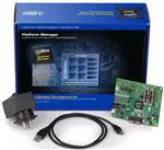


 工商网监
湘ICP备2023018690号
工商网监
湘ICP备2023018690号