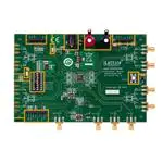
ispClock5400D Evaluation Board
User’s Guide
July 2010
Revision: EB50_01.2
�ispClock5400D Evaluation Board
User’s Guide
Lattice Semiconductor
Introduction
Thank you for choosing the Lattice Semiconductor ispClock™ device family!
This guide describes how to start using the ispClock5400D Evaluation Board, an easy-to-use platform for evaluating and designing with the ispClock5406D in-system-programmable differential clock distribution device. The evaluation board can be used stand-alone to review the performance and in-system programmability of the
ispClock5406D device or as a companion board and clock source for LatticeECP3™ FPGA evaluation boards:
• LatticeECP3 Serial Protocol Board
• LatticeECP3 Video Protocol Board
Please visit www.latticesemi.com/products/fpga/ecp3/ecp3evalboards for more information, demonstrations, and
documentation on each LatticeECP3 evaluation board.
About the ispClock5406D Device
This board features an ispClock5406D device that provides in-system-programmable zero delay universal fan-out
buffers for use in clock distribution applications. The on-board ispClock5406D is a 6-output clock distribution IC.
Differential ultra low skew outputs are organized with two banks per group. Each bank may be independently configured to support separate I/O standards (LVDS, LVPECL, HSTL, SSTL, HCSL, and MLVDS) and output frequency. In addition, each output provides independent programmable control of phase and time skew. All
configuration information is stored on-chip in non-volatile E2CMOS® memory.
The ispClock5406D devices provide extremely low propagation delay (zero-delay) from input to output using the
on-chip low jitter high-performance phase locked loop (PLL). A set of four fixed dividers can be used to generate
four frequencies derived from the PLL clock. These dividers are designed in powers of 2 only (2, 4, 8, and 16). The
clock output from any of the V-dividers can then be routed to any clock output pair through the output routing
matrix. The output routing matrix also enables routing of reference clock inputs directly to any output. For additional
details, please refer to the ispClock5400D Family Data Sheet.
Note: Static electricity can severely shorten the lifespan of electronic components.
• Use anti-static precautions such as operating on an anti-static mat and wearing an anti-static wristband.
• Store the evaluation board in the anti-static packaging provided.
• Always touch the SMA connector housing to equalize voltage potential between yourself and the board.
Features
The ispClock5400D Evaluation Board package includes:
• ispClock5400D Evaluation Board – The board features the following on-board components and circuits:
ispClock5406D programmable clock (ispPAC-CLK5406D-01SN48I)
– Crystal oscillator circuits
– Can oscillator circuit landing
– Resistor networks
– SMA connectors
– Power jack
– Test and JTAG interface headers
• Pre-loaded Base Demo – The kit includes a pre-loaded demo design that highlights key performance characteristics of the ispClock5406D device.
• Lattice ispDOWNLOAD™ Cable (HW-USBN-2A) – The ispDOWNLOAD cable provides a hardware connection
for in-system programming of the ispClock5406D device.
• User’s Guide – Provides information on powering, connecting lab equipment, and using the board as a clock
2
�ispClock5400D Evaluation Board
User’s Guide
Lattice Semiconductor
source for various Lattice FPGA evaluation boards. The contents of this user’s guide include demo operation,
top-level functional descriptions of the various portions of the evaluation board, descriptions of the on-board connectors, switches and a complete set of schematics.
• QuickSTART Guide – Provides information on connecting the evaluation board, running the pre-loaded evaluation demo.
The contents of this user’s guide include demo operation, programming instructions, top-level functional descriptions of the evaluation board, descriptions of the on-board connectors, switches and a complete set of schematics
of the board. For a complete list of the various connections and interfaces used on the ispClock5400D Evaluation
Board, please refer to the schematics in Appendix A.
The ispClock5400D Evaluation Board is 100% lead free and RoHS compliant as Lattice Semiconductor Corporation is sensitive to environmental issues.
Additional resources relating to the ispClock5400D Evaluation Board are available on the Lattice web site. Go to:
www.latticesemi/.com/boards and navigate to the appropriate link. Updates to this document can be found there,
as well as sample programs and links to other related items.
Figure 1. ispClock5400D Evaluation Board
Software Requirements
Install the following software before you begin developing designs for the ispClock5400D Evaluation Board:
• PAC-Designer® 5.2 (ispClock5406D support)
• Optional: ispLEVER®/Pro (LatticeECP3 support)
• Optional: ispVM™ System 17.5
3
�ispClock5400D Evaluation Board
User’s Guide
Lattice Semiconductor
Hardware Requirements
The following hardware is recommended for evaluation and demonstrations:
• Four matched SMA cables, SMA-to-BNC, 6 inches to 3 feet in length
• ESD strap or proper ESD test environment
• ispClock5400D Evaluation Board
• Lattice ispDOWNLOAD Cable
• AC wall adaptor for 5V DC output
• Optional: LatticeECP3 Serial Protocol Board (LFE3-95EA-SP-EVN)
• Optional: LatticeECP3 Video Protocol Board (LFE3-95EA-V-EVN)
• Optional: BERT Analyzer
• Optional: Agilent 8133A Clock Generator
• Optional: 4-channel, high-speed oscilloscope
Demonstration Designs
A common application of the ispClock5406D and a low-cost CMOS oscillator is to provide a low-jitter clock source
for SERDES-based applications in high-performance communications and computing equipment. The evaluation
board includes three demos that illustrate key applications of the ispClock5406D in the context of clock distribution
applications:
• ispClock5406D Base Demo – A pre-programmed, base demo of ispClock5406D features: low-jitter, time/phase
skew output control and I2C interface.
• Period Jitter Measurement – A demonstration of how to connect and measure ispClock5400D period jitter performance with a signal integrity analyzer.
• SERDES Reference Clock – A co-demonstration with the LatticeECP3 Serial Protocol or I/O Protocol boards.
• Video Reference Clock – A co-demonstration with the LatticeECP3 Video Protocol board.
Note: It is possible that you will obtain your evaluation board after it has been reprogrammed. To restore the factory
default demo and program it with other Lattice-supplied examples, see the Download Demo Designs section of this
document.
Base Demo of the ispClock5406D
The base demo consists of setting up the ispClock5400D Evaluation Board hardware and test equipment to demonstrate key features of the ispClock5406D device. The ability to adjust skew and frequency will be demonstrated
as well as programmable frequency, time and phase delay, reset functions and full dynamic control of internal registers through the on-board I2C bus interface.
Monitoring Clock Outputs
This section describes the procedure to monitor the evaluation board’s Bank 0 and Bank 2 clock outputs with a digital oscilloscope. Both banks are configured for LVDS output types.
To monitor clock outputs:
1. If you have not done so already, see the Programming the ispClock5400D Evaluation Board with ispVM section
of this document for details on set-up for the programming cable and applying power to the evaluation board.
4
�ispClock5400D Evaluation Board
User’s Guide
Lattice Semiconductor
2. Set DIP switches SW1 3 and 4 ON and all other switches OFF.
The blue LOCK LED lights to indicate the on-chip PLL is stable and locked to a reference clock.
3. Start PAC-Designer.
4. Choose File > Open…
The Open dialog appears.
5. Browse the Base_Demo_CLK5406D.PAC project and choose Open.
The ispPAC-CLK5406D schematic view appears.
Figure 2. ispClock5406D Schematic View
6. Choose File > Save As.
The Save As dialog appears.
7. Specify File name: Base_Demo_CLK5406D_rev.PAC and click Save.
PAC-Designer creates a new revision of the project.
8. Choose View > ispCLK Output Summary.
The Output Summary Sheet appears. The default demo will monitor the LVDS outputs driven by BANK_0 and
BANK_2.
Figure 3. Output Summary Sheet
5
�ispClock5400D Evaluation Board
User’s Guide
Lattice Semiconductor
9. If the board is not programmed with the demo project yet, press the Download icon on the top toolbar.
Figure 4. PAC-Designer Top Toolbar
The Frequency Summary dialog appears and reports the Reference and VCO frequency settings.
Figure 5. Frequency Summary Dialog Box
10. Click OK.
PAC-Designer reprograms the evaluation board with the updated JEDEC programming file.
11. Attach high-speed scope leads to the SMA sockets at BANK0 P, N and BANK2 P, N.
12. Set the scope input channel settings to 50 Ohm termination.
For this mode, we use LVDS and the 50 Ohm termination on each scope channel.
The waveforms shown are using 3’ long RG-316 cables with the SMA connectors. If the equipment has high
impedance probes or a differential probe, make sure that the LVDS BANK outputs have 100 Ohm termination
from BANK_P to BANK_N.
When operating properly, you should see four waveforms on the scope as shown in Figure 6. This represents
BANK0 and BANK2 output waveforms for both the BANK_P and BANK_N on each respectively. BANK0_P,N
are shown on the top pair, BANK2_P,N are shown on bottom pair. The full differential output would equal:
[BANK0_P minus BANK0_N] as well as on BANK2.
See the tables in the schematic (Appendix A) showing termination resistor options.
6
�ispClock5400D Evaluation Board
User’s Guide
Lattice Semiconductor
Figure 6. Scope Plot - Four Differential Outputs
Note: For user-designed boards and other applications, refer to the data sheet configurations and the schematics
of Appendix A. The schematic shows different resistor combinations for the different output bank settings. In LVDS
mode the schematic uses a single 100 Ohm resistor between each BANK_P and BANK_N pin as a fully differential
output. The demo uses the default factory board assembly with zero Ohm resistors connecting the SMA terminals
directly to the output banks. This approach is for the demo only. Some of the waveforms displayed will only show
the positive side of each BANK output on the scope for simplicity and timing measurements.
Modify Clock Time Skew
This section describes the procedure to modify the time skew of the ispClock5406D output to eliminate the inherent
skew between output BANK_0 and BANK_2 due to device and cable parasitic.
To modify clock time skew:
1. Adjust the scope to display BANK0_P and BANK2_P signals only. Overlap the signals to compare the relative
skew.
7
�ispClock5400D Evaluation Board
User’s Guide
Lattice Semiconductor
Figure 7. Scope Plot - Bank 0 and Bank 2 Overlapped
Note that a small inherent skew of the outputs plus any set-up delay in cables is about 50-80ps.
2. In PAC-Designer choose Tools > Design Utilities…
The Design Utilities dialog appears.
3. Choose ispPAC-CLK54_Skew_Editor.exe and click OK.
The ISPPAC-CLK5406D Skew Editor appears.
Figure 8. ispPAC-CLK5406D Skew Editor
The Skew Editor allows you to graphically configure the ispClock5406D output skew. Waveforms are color
coded. All disabled outputs are indicated in gray, while active outputs are indicated in green or white. Skew is
adjusted by dragging the waveform edges with the mouse. Dragging the waveform specified as feedback (highlighted in green) will move every other waveform in the opposite direction.
The Phase Skew steps are larger steps than the Time Skew. In the demo design, the “PUD” Phase Unit Delay,
has steps of 0.31 ns and there are 16 steps for each bank. For the demo, the Time Skew step is 18 ps.
8
�ispClock5400D Evaluation Board
User’s Guide
Lattice Semiconductor
4. Position the mouse over the rising edge of the Bank2 Time waveform.
The cursor will changes to a double-arrow icon to indicate a waveform edit.
5. Click and hold the Bank 2 Time waveform, then drag it three units to the right.
The Setting field displays 3 and Time Skew (ps) displays 54.00.
6. Click the Write to Schematic button.
PAC-Designer updates the time skew setting of the project.
7. Click the Download icon on the top toolbar.
The Frequency Summary dialog appears and reports the Reference and VCO frequency settings.
8. Click OK.
PAC-Designer reprograms the evaluation board with the updated JEDEC programming file.
9. Note the updated scope display.
This waveform shows the de-skewed outputs.
Figure 9. Scope Plot - De-skewed Outputs
The programmable ispClock5406D Time Skew feature allows the device to account for very small incremental
delays and correct for system/board trace-level effects. The function is used to correct timing delays and line up
edges to either account for PCB layout or to help with clock system timing such as the set-up and hold times of
the circuit being driven.
Experiment with the Time Skew and visualize the results on the scope. The demo design time skew range
allows you to move clock edges from 18 ps to 270 ps. When finished, set back to the Time-Skew that yields the
best results for your set-up.
9
�ispClock5400D Evaluation Board
User’s Guide
Lattice Semiconductor
Invert Clock Output
This section describes the procedure to invert the ispClock5406D output. In this procedure you will use the
ispClock5406D Invert feature to invert Bank2 output.
To invert a clock output:
1. From the PAC-Designer schematic view, double-click the BANK_2+/BANK_2- Output Block.
The Output Settings for BANK_2 & BANK_3 dialog box appears.
Figure 10. Output Settings for BANK_2 & BANK_3
2. Choose Inverted = Yes from the BANK_2 section of the dialog and click OK.
PAC-Designer updates the output setting of the project.
3. Click the Download icon on the top toolbar.
The Frequency Summary dialog appears and reports the Reference and VCO frequency settings.
4. Click OK.
PAC-Designer reprograms the evaluation board with the updated JEDEC programming file.
5. Note the updated scope display.
The waveform shows the inverted BANK_2 output.
10
�ispClock5400D Evaluation Board
User’s Guide
Lattice Semiconductor
Figure 11. Scope Plot - Inverted Output Bank
6. Repeat steps 1-4 to adjust the output bank to not invert the output (Inverted = No) and reprogram the device.
Modify Clock Phase Skew
This section describes the procedure to modify phase skew of the ispClock5406D output. The Phase skew Unit
Delay (PUD) is 0.31 ns for the demo design. In the following procedure the phase skew will be advanced four PUD
units or 1.24 ns.
To modify clock phase skew:
1. From PAC-Designer choose Edit > Symbol…
The Edit Symbol dialog appears.
2. Choose Skew Manager and click the Edit… button
Phase Skew Manager appears.
3. Choose the following options:
Skew Step = Fine
BANK_2 Phase Skew = 4PUD
Click OK.
PAC-Designer updates the phase skew for the project.
4. Click the Download icon on the top toolbar.
The Frequency Summary dialog appears and reports the Reference and VCO frequency settings.
5. Click OK.
PAC-Designer reprograms the evaluation board with the updated JEDEC programming file.
6. Note the updated scope display.
11
�ispClock5400D Evaluation Board
User’s Guide
Lattice Semiconductor
Figure 12. Scope Plot - Phase Skew Adjustment
The waveform shows the BANK_2 output advanced 1.24 ns.
Modify the Reference Clock Source Input
The evaluation board provides both 100 MHz (REFA) and 156.25 MHz (REFB) reference clock sources using onboard CMOS oscillators. This section demonstrates active clock selection using the ispClock5406D user-programmable control and status USER pins, to adjust the on-chip REFSEL signal. In this case, the user signal input
(USER3) acts as a mux control over REFA and REFB input reference clocks.
To modify the reference clock source input:
1. From PAC-Designer, double-click the USER Signal Routing Block.
The USER Pin Function Allocation dialog appears.
2. Note the REFSEL function input is set to the USER3 pin input.
This allows an external control over the ispClock5406D reference clock source input path.
3. Click Cancel.
4. Toggle position 3 of the DIP switch (USER3) on the evaluation board to the 0= (zero) position to enable the
156.25 MHz input reference clock, REFB_P/N input.
5. Note the updated scope display.
12
�ispClock5400D Evaluation Board
User’s Guide
Lattice Semiconductor
Figure 13. Scope Plot - 156.25 MHz Output
The 156.25 MHz clock from the REFB input output appears on the scope.
6. Toggle position 3 of the DIP switch (USER3) on the evaluation board back to the 1=REF-SEL position to
enable the 100 MHz input reference clock, REFA_P/N input.
In-System Changes via I2C Bus Interface
This section demonstrates the I2C status and control interface to the ispClock5406D device. The I2C interface feature allows you to override many device parameters of the device programming and make in-system changes to
almost all phase, time, reference and frequency settings of the ispClock5406D. The feature allows dynamic
time/phase skew for testing and margining of the output clocks, on every bank output pair. Upon device reset the
device returns to the configuration stored in E2CMOS.
The PAC-Designer I2C Design Utility for the ispClock5406D provides a software interface to the ispClock5406D I2C
registers such as output group and PLL controls.
The demo will apply all the changes you performed by reprogramming the device in the earlier procedures of the
user’s guide.
To set up the I2C ispDOWNLOAD Cable interface:
1. If you have not done so already, connect the ispDOWNLOAD cable to the I2C pin header (Appendix A,
Figure 41).
2. Start PAC-Designer.
3. Choose File > Open…
The Open dialog appears. (Note for PAC-Designer 5.2: See the Troubleshooting section of this user’s guide for
information on a correction required prior to using the I2C Design Utility.)
4. Browse the Base_Demo_CLK5406.PAC project and choose Open.
The ispPAC-CLK5406D schematic view appears.
5. From PAC-Designer choose Tools > Design Utilities…
The Design Utilities dialog appears.
13
�ispClock5400D Evaluation Board
User’s Guide
Lattice Semiconductor
Figure 14. Design Utilities Dialog Box
6. Select ispClock_5406_I2C_Utility.exe and click OK.
The ispClock5406D I2C Utility appears.
Figure 15. ispClock5406D I2C Utility
7. Choose Options > I2C Interface…
The Cable and I/O Port Setup Dialog appears.
14
�ispClock5400D Evaluation Board
User’s Guide
Lattice Semiconductor
8. Click the Change… button until the Uses PC USB Port title appears.
9. Disable the Bypass Hardware Checking (Demo Mode) option.
10. Click the Settings… button.
The USB Settings dialog appears.
11. From the Select USB port name… section, choose Search for download cable on all USB ports and click
Connect Now.
The I2C utility indicates when the USB connection is made. Click OK.
12. From the Cable and I/O Port Setup dialog, click OK.
13. From the ispClock5406D I2C Utility click the I2C Address = … button.
The ispClock5406 I2C Address dialog appears.
Figure 16. ispClock5406D I2C Address Dialog Box
14. Select 7Fh from the I2C Address list and click OK.
The I2C Utility sets the I2C address for the ispClock5406D.
The 5406D I2C device address must match what is stored in E2CMOS when the device program was downloaded with the JTAG pattern. Once the address is set, full communication can be established with the device
using the I2C interface.
Note: Make sure the ispDOWNLOAD cable is moved to the I2C port header J15 on the evaluation board.
To apply an in-system output change:
1. If you have not done so, connect the evaluation board to a scope and adjust the display using the procedure in
the Modify Clock Time Skew section of this document.
2. Adjust the scope to display BANK0_P and BANK2_P signals only. Overlap the signals to compare the relative
skew.
15
�ispClock5400D Evaluation Board
User’s Guide
Lattice Semiconductor
Figure 17. Scope Plot - Skew Measurement
Note a small inherent skew of the outputs plus any set-up delay in cables is about 50-80ps.
3. From the ispClock5406D I2C Utility click the Output Group 1 button.
The ispClock5406D Output Group 1 Control dialog appears.
Figure 18. ispClock5406D Output Group 1 Control
The I2C utility output group control supports in-system changes to:
- V-Dividers settings/routing for each bank
- Phase-Skew enable
- Output Bank enable, OE control
16
�ispClock5400D Evaluation Board
User’s Guide
Lattice Semiconductor
- Ref Select, reference A or B MUX control
- Phase–Skew value, 16 values
- Output Delay Mode for Zero-Delay mode or FOB, Fan-Out Buffer mode
4. Double-click the Bank 2 output block (0x0, 8 TUD, 0=Disable) of the schematic.
The Output Group-1 Bank 2 Time Skew dialog appears.
5. Specify 3 and click OK.
The output block display is updated to 0xB, 3 TUD, 0=Disable to indicate the new configuration of the block.
6. From the ispClock5406D Output Group 1 Control dialog click the Write button.
The I2C utility writes the control registers to the ispClock5406D I2C interface and updates the time skew by
three steps (18 ps x 3 = 54 ps).
7. Note the updated scope display.
The BANK0_P and BANK2_P outputs will be de-skewed in the same manner as the reprogrammed device
demonstrated in section 6.1.2 Modify Clock Time Skew of the user’s guide. The value is written to the register
and active at this point unless an I2C soft or full reset or hardware power on reset occurs.
For more information on I2C control registers, see the ispClock5400D Family Data Sheet.
8. From the ispClock5406D Output Group 1 Control dialog click the OK button.
You may wish to experiment with the I2C utility interface to apply the same clock inversion and phase skew
changes as documented in the Invert Clock Output and 6.1.4 Modify Clock Phase Skew section of this document.
To reset the ispClock5406D device via the I2C interface:
1. From the ispClock5406D I2C Utility, click the Soft Reset button.
The ispClock5406D Soft Reset dialog prompt appears and the I2C utility issues the I2C command to assert soft
reset. During this state the PLL, Dividers, Phase and Time Skew blocks are reset. The differential outputs of
the ispClock5406D banks disabled during the soft reset state.
Figure 19. ispClock5406D Soft Reset Dialog - Soft Reset State
2. Click OK.
3. Click the Soft Reset button.
The ispClock5406D Soft Reset dialog prompt appears and the I2C utility issues the I2C command to release
soft reset.
17
�ispClock5400D Evaluation Board
User’s Guide
Lattice Semiconductor
Figure 20. ispClock5406D Soft Reset Dialog - Soft Reset Released State
4. Click OK.
Note the scope display changes to reflect the time-skewed waveform pattern produced earlier. I2C commands
will be retained and reapplied after soft reset has been released.
5. Click the Full Reset button.
The ispClock5406D Full Reset dialog prompt appears and the I2C utility issues the I2C command to assert full
reset. During this state, all configuration registers are updated from the E2CMOS configuration. All the values
loaded by I2C are overwritten. This command is equivalent to toggling the RESETb pin of the ispClock5406D
device. The differential outputs of the ispClock5406D banks are disabled during the full reset state.
6. Click OK.
7. Click the Full Reset button.
The ispClock5406D Full Reset dialog prompt appears and the I2C utility issues the I2C command to release full
reset. When released from a full reset the device reverts back to the configuration state that is defined and
stored in E2CMOS.
8. Click OK.
Note the scope display changes to reflect the original waveform pattern produced by the initial ispClock5406D
device programming.
You have completed the ispClock5406D Base Demo. You can try other in-system device configurations using the
I2C utility or modify the PAC-Designer project then reprogram the device.
Period Jitter Measurement
The demo consists of setting up the ispClock5400D Evaluation Board hardware and a Wavecrest (Gigamax) SIA3000D analyzer to demonstrate the ultra-low phase jitter of the ispClock5406D device.
How to set up the SIA-3000D:
1. From the SIA-3000D, GigaView software, perform Extended Timer Calibration (>=11min calibration).
2. Open the Clock Analysis Tool and set up for a Period Jitter measurement.
Set up the base demo project for a phase jitter measurement:
1. Use PAC-Designer to open the Base_Demo_CLK5406D.PAC project.
2. Save the Base_Demo_CLK5406D.PAC as Base_Demo_CLK5406D_jitter.pac.
3. Choose Edit > Symbol...
The Edit Symbol dialog appears.
4. Choose REF Frequency and click Edit...
The PLL Core Settings dialog appears.
18
�ispClock5400D Evaluation Board
User’s Guide
Lattice Semiconductor
5. Specify REF Frequency: 100 then click the Internal Feedback, Modify... button.
The External Feedback Setting dialog appears.
6. Select Internal Feedback, select Feedback taken from V-Divider 8, and click OK.
7. From the PLL Core Settings dialog, click OK.
8. From the Edit Symbol dialog, select USER PINS and click the Edit... button.
The USER Pin Function Allocation dialog appears.
9. Select PLL_BYPASS = PLL then click the OK button.
The USER Pin Summary dialog appears. Click the OK button.
10. From the Edit Symbol dialog select Output BANK_0 then click the Edit... button.
The Output Settings for BANK_0 & Bank_1 dialog appears.
11. Click the Source, Modify... button.
The Output Pair Source Setting dialog box appears.
12. For BANK_0, choose V-Divider-8, choose, From V-Divider, and click the OK button.
From the Output Settings for BANK_0 & BANK_1 dialog, select the following options for BANK_0:
Output Type: LVPECL
Output Enable: Always Enabled
Select the following option for BANK_1:
Output Enable: Always Disabled
Click the OK button.
13. From the Edit Symbol dialog select Output BANK_2 then click the Edit... button.
The Output Settings for BANK_2 & Bank_3 dialog appears.
14. From the Output Settings for BANK_2 & BANK_3 dialog, select the following options for BANK_2:
Output Enable: Always Disabled
Select the following option for BANK_3:
Output Enable: Always Disabled
Click the OK button.
15. From the Edit Symbol dialog select Output BANK_4 then click the Edit... button.
The Output Settings for BANK_4 & Bank_5 dialog appears.
16. From the Output Settings for BANK_4 & BANK_5 dialog, select the following options for BANK_4:
Output Enable: Always Disabled
Select the following option for BANK_5:
Output Enable: Always Disabled
Click the OK button.
17. From the Edit Symbol dialog, click Close.
18. Click the Download icon on the top toolbar.
The Frequency Summary dialog appears and reports the Reference and VCO frequency settings.
19. Click OK.
PAC-Designer reprograms the evaluation board with the updated JEDEC programming file.
19
�ispClock5400D Evaluation Board
User’s Guide
Lattice Semiconductor
Set up the evaluation board for a phase jitter measurement:
1. Set the evaluation board DIP switches to enable 3.3V VCCO.
2. Enable the REFA Oscillator input.
3. Disable the REFB Oscillator input.
4. Set the REF_SEL switch to 0.
5. Connect the BANK0 differential outputs to the SIA-3000D differential inputs.
6. From the SIA-3000D GigaView software, execute Pulse Find.
7. Initiate Clock Analysis measurement. Typical phase jitter for the ispClock5406D is 2.5ps.
SERDES Clock Source for LatticeECP3 Serial Protocol Board Demo
AN6081, Driving SERDES Devices with the ispClock5400D Differential Clock Buffer, describes the low-jitter performance characteristics of the ispClock5406D clock output in the context of a XAUI application. SMA connections
J29, J33 and J30, J34 of the LatticeECP3 Serial Protocol Board allow you to connect the SMA outputs of the
ispClock5400D Evaluation Board as high-quality clock source.
Video Clock Source for LatticeECP3 Video Protocol Board Demo
AN6081, Driving SERDES Devices with the ispClock5400D Differential Clock Buffer, describes the low-jitter performance characteristics of the ispClock5406D clock output in the context of a 270 MHz SDI video application.
This demonstration requires Lattice Intellectual Property for the LatticeECP3 FPGA. Please contact Lattice for
more information on how to obtain the project source.
Download Demo Designs
The ispClock5406D base demo is preprogrammed into the evaluation board, however over time it is likely your
board will be modified. Lattice distributes source and programming files for demonstration designs compatible with
the evaluation board.
To download demo designs:
1. Browse to the ispClock5400D Evaluation Board web page of the Lattice web site. Select the Demo Applications download and save the file.
Extract the contents of Base_Demo_CLK5406.zip to an accessible location on your hard drive.
Export an ispClock5406D JEDEC with PAC-Designer
Use the procedure below to re-export a JEDEC programming file for any ispClock5406D demo project for the evaluation board.
1. Install and license PAC-Designer software (www.latticesemi.com/products/designsoftware/pacdesigner).
2. Download the demo source files from the ispClock5400D Evaluation Board web page.
3. Run PAC-Designer.
4. Open the .pac project file.
5. Choose File > Export… The Export dialog appears.
6. Select Export What: Jedec File.
20
�ispClock5400D Evaluation Board
User’s Guide
Lattice Semiconductor
7. Click the Browse… button. The Save As dialog appears.
8. Browse to the destination folder, specify a file name, and click Save.
9. Click OK. After a few moments the JEDEC programming file is output.
10. See the Programming with PAC-Designer section of this document for details on downloading a programming
file to the board.
Programming the ispClock5400D Evaluation Board with PAC-Designer
To restore the ispClock5406D to factory settings or load an alternative demo design, use the procedure in this section to reprogram the evaluation board using PAC-Designer software.
Programming for the ispClock5406D device is controlled using PAC-Designer or the ispVM System software, available for download from the Lattice website at www.latticesemi.com/ispvm. Refer to the ispVM System software for
help regarding operation of this software.
JTAG programming is supported with the eight-pin connector J14 and either the Lattice ispDOWNLOAD USB
download cable (HW-USBN-2A, provided) or the parallel download cable (HW-DLN-3C). PAC-Designer provides
an interface to configure the ispClock5406D and can be used to either directly program the evaluation board or to
export a JEDEC • le which can be used with ispVM to program the evaluation board.
The board must be un-powered when connecting, disconnecting, or reconnecting the ispDOWNLOAD Cable.
Always connect the ispDOWNLOAD Cable’s GND pin (black wire) before connecting any other JTAG pins. Failure
to follow these procedures can in result in damage to the ispClock5406D device and render the board inoperable.
Connecting Programming Cable and a Power Source
To connect the ispClock5400D Evaluation Board to your PC:
1. Plug the ispDOWNLOAD Cable into the USB port on the PC.
2. Plug the JTAG color-coded wires of the ispDOWNLOAD cable in the order marked on the board’s JTAG interface header (J14) before applying power. The cable comes with an 8-pin adapter for 1x8. This will allow you to
maintain the order and simplifies moving it to other ports.
3. Plug the power cord in and insert the connector into the Power Jack (J13).
Once the board is powered up, you will see the green LED labeled POWER. This LED is lit when the AC
adapter is plugged in or if the board is powered by the +12V red and black banana receptacles.
Set up the Programming Cable Interface
To setup the ispDOWNLOAD cable interface:
1. Run PAC-Designer.
2. Choose Options > Cable and I/O Port Set-up.
The Cable and I/O Port Setup dialog appears.
3. From the Programming Cable Interface section, click the Change... button.
The Change Programming Cable Interface dialog appears.
21
�ispClock5400D Evaluation Board
User’s Guide
Lattice Semiconductor
Figure 21. Change Programming Cable Interface Dialog Box
4. From the Programming Cable Interface list, select Uses PC USB and click OK.
The Cable and I/O Port Setup dialog appears.
Figure 22. Cable and I/O Port Setup Dialog Box
5. Click Settings…
The USB Setting dialog appears.
22
�ispClock5400D Evaluation Board
User’s Guide
Lattice Semiconductor
Figure 23. USB Settings Dialog Box
6. Enable Connect at startup and click OK.
An information dialog appears. After altering the USB setting within these dialog boxes, PAC-Designer must be
restarted to load the port drivers for the system.
Figure 24. PAC-Designer JTAG Prompt
7. Click OK to dismiss the message.
8. Close PAC-Designer.
Programming the Evaluation Board
To repgrogram the ispClock5400D Evaluation Board:
1. Run PAC-Designer.
2. Open the .pac project file.
3. Choose Tools > Download
The Frequency Summary dialog appears and reports the Reference and VCO frequency settings.
23
�ispClock5400D Evaluation Board
User’s Guide
Lattice Semiconductor
Figure 25. Frequency Summary Dialog Box
4. Click OK.
PAC-Designer reprograms the evaluation board with the updated JEDEC programming file.
ispClock5400D Evaluation Board
This section describes the features of the ispClock5400D Evaluation Board in detail. The features appear in alphabetical order.
DIP Switch
To simplify the use of the evaluation board an 8-position DIP switch (SW1) is provided for common adjustments.
The switch can be roughly divided into four sections: reference oscillator control, PLL control, output enables, and
VCCO control. Table lists the switches and their respective functions. Note that for switch sections 6, 7, and 8 only
one should be on at a time. The default setting with all the switches to the left (OFF) enables the on-board oscillator, selects that as the clock reference, and allows the PLL to lock to that frequency.
Table 1. DIP Switch Functions
To the Left
SW1 – Section
To the Right
0=
1
1=REFA_EN
0=
2
1=REFB_EN
0=
3
1=REF-SEL
LOCK-LED
4
N/C=USER0
Unused
5
Unused
2.5V
6
3.3V
1.8V
7
3.3V
1.5V
8
3.3V
Input/Output Connections
The evaluation board incorporates tapered transitions from the SMA connectors to the matched 50-ohm microstrip
transmission lines. All of the output transmission lines are matched in length to the sense signals (REFA, REFB,
and FEEDBACK) to support accurate timing measurements both for bank-to-bank and input-to-output. The header
at J16 (Appendix A, Figure 41) provides access to the essential control and monitor pins of the ispClock5406D
such as REFA_EN, REFB_EN, USER0, USER3, REFB_VTT, VCCO, and FBK_VTT.
Off-Board Clock Connections
An off-board CMOS clock can be used by connecting to the REFB_P (J2) SMA connector (Appendix A, Figure 35).
When using a CMOS reference clock, the negative differential input must be biased to VCC/2. For REF_B this is
done by populating R5, R7, and C53.
24
�ispClock5400D Evaluation Board
User’s Guide
Lattice Semiconductor
The ispClock5406D can also be driven from an external differential clock source by moving the zero-ohm resistor
from the R35 location to the R37 location and connecting the clocks to both REFB_N and REFB_P inputs (J1 and
J2). When an external clock source is used, switches 1 and 2 of DIP-switch SW1 (Appendix A, Figure 34) should
be in the left position to disable both on-board oscillators. When an external clock is used for REFB_P (J2), zero
ohm resistors must be used for R13 and R11 and R10 should be removed. If an external clock is used for REFB_N
(J1), then zero ohm resistors must be used for R14 and R12, and R15, R9, R7, and R5 should be removed.
On-Board Termination
The ispClock5400D Evaluation Board is designed to support a variety of on-board termination schemes. The board
comes from the factory with zero-ohm jumpers in place of the on-board termination in order to support off-board
termination and quick validation of designs with an oscilloscope. In this section we will detail the various termination schemes using output Bank-0 as the example. The other three output banks have similar circuits and reference
numbering to promote ease of use.
At first glance, the schematic shown in Appendix A, Figure 36 (or any sheet containing the output bank schematics)
appears to have too many parts between the ispClock5406D outputs and the SMA connectors. However, only
some of the parts are required for any particular output mode. So, for any given output mode there will be several
unpopulated parts. Each output mode will be covered in detail in the following sections.
All the passive devices used in the termination have SMD 0605 footprints. R28 and R29 are not mislabeled, in
more cases the positions are populated with resistors but, in other cases DC blocking capacitors. The on-board TLine and termination networks support differential viewing of the signal at the end of the T-Line. In cases where
only one output of the signal is to be viewed (connected to a scope) the other output should be terminated with a
similar length of cable and a 50 ohm terminator.
LVDS
Low Voltage Differential Signal (LVDS) termination requires 100 ohms differential at the end of the transmission
line. The network shown at the end of the T-line in Figure 26 provides the required termination impedance and
sends a portion of the waveform off board to a scope. The sum of R23, R25, R26, and R24 add up to 110 ohms
which is 10 ohms too much. However, the AC coupling provided by R28, and R29 brings the scope impedance and
the series resistors R30 and R31 in parallel with R25 and R26 (168 || 44 = 34.87). This effectively lowers the
impedance seen at the end of the T-line to about 101 ohms and provides a divider network to sample the signal at
the scope without causing reflections or an impedance miss-match. The divider ratio is about 4.75:1 and can be
verified by measuring the voltage at the end of the T-line with an amplified high frequency probe on the scope.
Figure 26. Bank 0 LVDS with On-Board Termination
ispClock
Scope
R16
On Board T-Line
R28
R23
BANK_0P
J3
R30
50 ohms / 64.3 mm
0
33
On Board T-Line
R24
R25
22
0.1uF
R26
22
R29
34
5pF
R31
50 ohm s / 64.3 m m
0
50
50 ohms / 91 cm
LVDS
Buffers
R17
SMA to BNC Cable
SMA to BNC Cable
50
50 ohm s / 91 c m
33
0.1uF
34
5pF
J4
BANK_0N
ispClock5406D Standard Evaluation Board
MLVDS
Multi-drop LVDS (MLVDS) termination incorporates a differential source termination resistor in addition to standard
LVDS termination. Figure 27 shows R18 providing the source termination at the driven side of the T-Line. At the
receiving end of the on-board T-Line, the termination and scope sense circuit is identical to that of LVDS circuit discussed above.
25
�ispClock5400D Evaluation Board
User’s Guide
Lattice Semiconductor
Figure 27. Bank 0 MLVDS with On-Board Termination
Scope
ispClock
On Board T-Line
R16
R28
R23
BANK_0P
J3
R30
50 ohms / 64.3 mm
0
MLVDS
Buffers
SMA to BNC Cable
50
50 ohms / 91 cm
33
R25
22
0.1uF
R26
22
R29
34
5pF
R18
100
On Board T-Line
R17
R24
R31
50 ohm s / 64.3 m m
0
SMA to BNC Cable
50
50 ohm s / 91 c m
33
0.1uF
34
5pF
J4
BANK_0N
ispClock5406D Standard Evaluation Board
LVPECL
LVPECL drivers require a DC bias at the driven end of the T-Line and 100 ohms differential termination at the
receiving end of the T-Line. The DC bias is usually provided by 50 ohms impedance to VCCO-2V. This will both
bias the output buffers and terminate one end of the T-Line to minimize reflections. In Figure 28, R19 with R21 and
R20 with R22 function as voltage dividers to provide the required bias and termination. With a 3.3V VCCO supply
the divided voltage is 1.3V and the Thevenin-equivalent impedance seen by the T-Line is 50 ohms (82 || 124 = 50).
At the receiving end of the on-board T-Line, the termination and scope sense circuit is identical to that of LVDS circuit discussed above.
Figure 28. Bank 0 LVPECL with On-Board Termination
VCCO
ispClock
R21
124
On Board T-Line
R16
R28
R23
BANK_0P
J3
R30
50 ohms / 64.3 mm
0
LVPECL
Buffers
50
50 ohms / 91 cm
33
R19
82
Scope
SMA to BNC Cable
VCCO
R25
22
0.1uF
R26
22
R29
34
5pF
R22
124
On Board T-Line
R17
R24
R31
50 ohm s / 64.3 m m
0
R20
82
SMA to BNC Cable
50
50 ohm s / 91 c m
33
0.1uF
34
5pF
J4
BANK_0N
ispClock5406D Standard Evaluation Board
SSTL15/SSTL18
SSTL15 and SSTL18 both utilize the same termination network, which is 50 ohms at the receiving end of the T-Line
to VCCO divided by 2. Figure 29 shows that for the ispClock5406 a source termination of 20 ohms is also recommended and provided by R16 and R17. At the load end of the non-inverting T-Line the output supply VCCO is
divided in half using the network of R33 on the top side and R23, R25, R28, and the scope input impedance on the
bottom side. The lower half of this divider is a 5:1 sub-divider for viewing the waveform at the scope. The inverting
output has a similar circuit to provide a balanced load at the end of the T-Line and to support viewing both sides of
the differential signal.
26
�ispClock5400D Evaluation Board
User’s Guide
Lattice Semiconductor
Figure 29. Bank 0 SSTL15/SSTL18 with On Board Termination
VCCO
ispClock
Scope
R33
100
R16
On Board T-Line
R28
R23
BANK_0P
J3
R30
50 ohms / 64.3 mm
71.5
VCCO
On Board T-Line
R25
45.3
18.7
0
5pF
R27
0
R32
100
R17
50
50 ohms / 91 cm
20
SSTL
Buffers
SMA to BNC Cable
R24
R26
45.3
R29
R31
50 ohms / 64.3 mm
SMA to BNC Cable
50
50 ohms / 91 cm
20
71.5
18.7
0
5pF
J4
BANK_0N
ispClock5406D Standard Evaluation Board
SSTL25
Figure 30 shows the only difference from SSLT15/SSTL18 and SSTL25 is the source termination R16 and R17
increases from 20 ohms to 25 ohms. The remainder of the circuit is the same as SSTL15/SSTL18, discussed
above.
Figure 30. Bank 0 SSTL25 with On-Board Termination
VCCO
ispClock
Scope
R33
100
R16
On Board T-Line
R28
R23
BANK_0P
J3
R30
50 ohms / 64.3 mm
71.5
VCCO
On Board T-Line
R25
45.3
18.7
0
5pF
R27
0
R32
100
R17
50
50 ohms / 91 cm
25
SSTL
Buffers
SMA to BNC Cable
R24
R26
45.3
R29
R31
50 ohms / 64.3 mm
SMA to BNC Cable
50
50 ohms / 91 cm
25
71.5
18.7
0
5pF
J4
BANK_0N
ispClock5406D Standard Evaluation Board
eHSTL/HSTL
For eHSTL and HSTL the source termination resistance R16 and R17 drops to zero ohms as shown in Figure 31.
The remainder of the termination and sensing circuitry is the same as for SSTL.
Figure 31. Bank 0 eHSTL/HSTL with On Board Termination
VCCO
ispClock
Scope
R33
100
R16
On Board T-Line
R28
R23
BANK_0P
J3
R30
50 ohms / 64.3 mm
71.5
VCCO
On Board T-Line
R25
45.3
18.7
0
5pF
R27
0
R32
100
R17
R24
R26
45.3
R29
R31
50 ohms / 64.3 mm
0
50
50 ohms / 91 cm
0
HSTL
Buffers
SMA to BNC Cable
SMA to BNC Cable
50
50 ohms / 91 cm
71.5
18.7
0
5pF
J4
BANK_0N
ispClock5406D Standard Evaluation Board
27
�ispClock5400D Evaluation Board
User’s Guide
Lattice Semiconductor
HCSL
HCSL termination involves a bias network to ground at the driver and no termination at the end of the T-Line.
Figure 32 shows the drivers biased through series resistors R16 and R17 (value of 33 ohms) combined with resistors R19 and R20 (value of 50 ohms). R19 and R20 also provide T-Line source termination. The receiving end of
the T-Line does not require any termination. The sense resistors R28 and R29 (value 950 ohms) are not low
enough to serve as termination loads but, provide a way to view the waveforms on the scope. The scope input
impedance combined with R28 and R29 result in a 20:1 divider of the waveforms at the end of the T-Line.
Figure 32. Bank 0 HCSL with On-Board Termination
ispClock
On Board T-Line
R16
R28
R23
BANK_0P
J3
R30
50 ohms / 64.3 mm
33
Scope
SMA to BNC Cable
50
50 ohms / 91 cm
0
950
0
5pF
HCSL
Buffers
R19
50
R20
50
On Board T-Line
R17
R29
R24
R31
50 ohms / 64.3 mm
33
SMA to BNC Cable
50
50 ohms / 91 cm
0
950
0
5pF
J4
BANK_0N
ispClock5406D Standard Evaluation Board
Power Supply Connections
The evaluation board is powered by a 12V to 5V power supply capable of providing one ampere or more. The
board can be powered either by a wall adapter with a 2.5mm coaxial power plug at J13 or from a bench supply with
banana plugs at J11 and J12. Once onboard, the supply is regulated (U2) to provide the 3.3V supply needed for
VCCD, VCCA, and VCCJ.
A second adjustable regulator (U3) provides the VCCO for banks 3 and 5 and it is programmable using the onboard resistors and three of the DIP switches of SW1. To bypass the on-board regulators, zero ohm resistors R106
and R116 can be removed from the board to allow external supplies to power the ispClock5406D.
Troubleshooting
PAC-Designer 5.2: The ispClock5406D PLL Control dialog box of the ispClock5406D I2C Utility
(ispClock_5406_I2C_Utility.exe) appears corrupted and the background color obscures the schematic
view.
To correct the display:
1. Exit the ispClock5406D I2C Utility.
2. From Windows, browse to the \PAC-Designer52\Macro folder of the PAC-Designer installation directory.
3. Locate the following files:
ispClock_5406_I2C_OutGroup_BI_Sch.emf
ispClock_5406_I2C_OutGroup_LI_Sch.emf
ispClock_5406_I2C_OutGroup_UI_Sch.emf
ispClock_5406_I2C_OutGroup_Sch.emf
ispClock_5406_I2C_PLL_Sch.emf
4. Rename each file so they appear as:
ispClock_5400_I2C_OutGroup_BI_Sch.emf
ispClock_5400_I2C_OutGroup_LI_Sch.emf
ispClock_5400_I2C_OutGroup_UI_Sch.emf
28
�ispClock5400D Evaluation Board
User’s Guide
Lattice Semiconductor
ispClock_5400_I2C_OutGroup_Sch.emf
ispClock_5400_I2C_PLL_Sch.emf
5. Rerun the ispClock5406D I2C Utility.
Environmental Requirements
The evaluation board must be stored between -40°C and 100°C. The recommended operating temperature is
between 0°C and 55°C.
The evaluation board can be damaged without proper anti-static handling.
Pin Information and Bank Summary
This section describes the pin information for the ispClock5406D device and board connections.
Table 2. Pin Information and Bank Summary
Pin #
Pin Function
Bank
Board Connection
1
GNDO_5
5
GND
2
BANK_5P
5
BANK_5P
3
BANK_5N
5
BANK_5N
4
VCCO_5
5
VCCO_5
5
VCCO_4
4
VCCO_4
6
BANK_4P
4
BANK_4P
7
BANK_4N
4
BANK_4N
8
GNDO_4
4
GND
9
GNDO_3
3
GND
10
BANK_3P
3
BANK_3P
11
BANK_3N
3
BANK_3N
12
VCCO_3
3
VCCO_3
13
GNDA
GND
14
REFAVTT
GND
15
REFAN
REFA_N
16
REFAP
REFA_P
17
REFBVTT
REFB_VTT
18
REFBN
REFB_N
19
REFBP
REFB_P
20
FBKVTT
FBK_VTT
21
FBKN
FBK_N
22
FBKP
FBK_P
23
VCCA
VCCA
24
RREF
25
VCCO_2
2
VCCO_2
26
BANK_2N
2
BANK_2N
27
BANK_2P
2
BANK_2P
28
GNDO_2
2
GND
29
GNDO_1
1
GND
30
BANK_1N
1
31
BANK_1P
1
32
VCCO_1
1
33
VCCO_0
0
29
VCCO_0
�ispClock5400D Evaluation Board
User’s Guide
Lattice Semiconductor
Table 2. Pin Information and Bank Summary (Continued)
Pin #
Pin Function
Bank
Board Connection
34
BANK_0N
0
BANK_0N
35
BANK_0P
0
BANK_0P
36
GNDO_0
0
GND
37
VCCJ
VCC
38
TDO
TDO
39
TMS
TMS
40
TCK
TCK
41
TDI
TDI
42
RESETb
RESETb
43
GNDD
GND
44
VCCD
VCC
45
USER3
USER3
46
USER2
SCL
47
USER1
SCA
48
USER0
USER0
Note: ispClock5400D Family Data Sheet version 01.2, November 2009.
Glossary
I2C: Inter-Integrated Circuit.
LED: Light-Emitting Diode.
PCB: Printed Circuit Board.
RoHS: Restriction of Hazardous Substances Directive.
PLL: Phase Locked Loop.
References
The following documentation is recommended for evaluation and demonstrations:
• AN6080: Using a Low-Cost CMOS Oscillator as a Reference Clock for SERDES Applications
• AN6081: Driving SERDES Devices with the ispClock5400D Differential Clock Buffer
• EB44: LatticeECP3 Serial Protocol Board User’s Guide
• EB39: LatticeECP3 Video Protocol Board User’s Guide
Ordering Information
Description
ispClock5400D Evaluation Board
Ordering Part Number
PACCLK5406D-S-EVN
30
China RoHS Environment-Friendly
Use Period (EFUP)
�ispClock5400D Evaluation Board
User’s Guide
Lattice Semiconductor
Technical Support Assistance
Hotline: 1-800-LATTICE (North America)
+1-503-268-8001 (Outside North America)
e-mail: techsupport@latticesemi.com
Internet: www.latticesemi.com
Revision History
Date
Version
December 2009
01.0
Initial release.
Change Summary
December 2009
01.1
Added Troubleshooting section.
July 2010
01.2
Updated part numbers for the LatticeECP3 Serial Protocol Board and
LatticeECP3 Video Protocol Board in the Hardware Requirements section.
© 2010 Lattice Semiconductor Corp. All Lattice trademarks, registered trademarks, patents, and disclaimers are as
listed at www.latticesemi.com/legal. All other brand or product names are trademarks or registered trademarks of
their respective holders. The specifications and information herein are subject to change without notice.
31
�A
B
C
D
R34
FBK_N
J17
FBK_P
J18
5
C3
100nF
TDO
TMS
TCK
TDI
FBK_VTT
REFB_P
REFB_N
REFB_VTT
REFA_P
REFA_N
Sheet 9 {
Sheet 3 {
Sheet 2 {
470
C54
100nF
RESETb
USER0
SDA
SCL
USER3
C2
C1
Sheet 9 {
100nF
TDO
TMS
TCK
TDI
FBKP
FBKN
FBKVTT
REFBP
REFBN
REFBVTT
REFAP
REFAN
REFAVTT
RREF
RESETb
USER0
USER1
USER2
USER3
ispCLOCK5406D
VCCO_5
BANK_5P
BANK_5N
GNDO_5
VCCO_4
BANK_4P
BANK_4N
GNDO_4
VCCO_3
BANK_3P
BANK_3N
GNDO_3
VCCO_2
BANK_2P
BANK_2N
GNDO_2
VCCO_1
BANK_1P
BANK_1N
GNDO_1
VCCO_0
BANK_0P
BANK_0N
GNDO_0
3
4
2
3
1
5
6
7
8
12
10
11
9
25
27
26
28
32
31
30
29
33
35
34
36
4
3
Connect DIEPAD to ground plane with 5 or more vias.
38
39
40
41
22
21
20
19
18
17
16
15
14
24
42
48
47
46
45
U1
DIE_PAD
49
100nF
44
VCCD
VCC
37
VCCJ
GNDD
43
4
23
VCCA
GNDA
32
13
5
Date:
Size
A
2
Thursday, February 19, 2009
Project
ispClock5406D Lab Evaluation Board
Sheet
Lattice Semiconductor Applications
Email: techsupport@Latticesemi.com
Phone (503) 268-8001 -or- (800) LATTICE
} Sheet 7
} Sheet 6
} Sheet 5
} Sheet 4
} Sheet 2
Title
ispCLOCK5406D
VCCO_5
BANK_5P
BANK_5N
VCCO_3
BANK_3P
BANK_3N
VCCO_2
BANK_2P
BANK_2N
VCCO_0
BANK_0P
BANK_0N
VCCA
2
1
1
B
B
Schematic Rev
Board Rev
of 9
1
A
B
C
D
Lattice Semiconductor
ispClock5400D Evaluation Board
User’s Guide
Appendix A. Schematic
Figure 33. ispClock5406D
�33
A
B
C
D
C4
1uF
VCC
R107
100k
4
R109
100k
6
2
1
OUTP
OUTN
3
SW1D
SW1C
SW1B
13
14
15
16
GND
SW1A
EN
VCC
R111
100k
1
4
C6
10nF
USER0
C5
100nF
5x7 Oscillator
X1
3
10uH
L1
C50
100nF
VCC
4
USER3
5
REFB_EN
REFA_EN
VCC
5
5
LOCK
D5
R112
R110
R108
4
1k
1k
1k
10uH
L9
C51
10nF
R3
R1
3
1K
R113
VCC
VCCA
Connect at
Crystal Ground
3
R2
C10
330pF
100nF
C12
Date:
Size
A
Thursday, February 19, 2009
Project
ispClock5406D Lab Evaluation Board
2
124
X
220
10uH
L3
X = Do Not Install
LVPECL
LVDS
LVCMOS
Xtal Output R1
Sheet
1
1
B
B
82
X
X
R4
Board Rev
of 9
2
124
X
220
R3
Schematic Rev
VCC
82
X
X
R2
Lattice Semiconductor Applications
Email: techsupport@Latticesemi.com
Phone (503) 268-8001 -or- (800) LATTICE
C11
10nF
REFA_P
REFA_N
Title
ispClock5406D Reference Oscillator "A"
R4
VCC
2
A
B
C
D
Lattice Semiconductor
ispClock5400D Evaluation Board
User’s Guide
Figure 34. ispClock5406D Reference Oscillator “A”
�34
A
B
C
D
X
X
Can X3 Diff
J1 & J2
5
X
Can X3 SE
R15
C48
100nF
C8
100nF
C49
10nF
C9
10nF
4
X
X
X
0
0
0
0
X
0
0
X
X
0
X
X
X
0
X
X
X
4
X
X
0
X
7
14
X3
3
GND
OUTP
OUTN
R13
R14
EN/OUTN
OUTP
Can Oscillator
EN
VCC
GND
REFB_P
J2
6
1
5x7 Oscillator
X2
VCC
REFB_N
J1
R10 R11 R12 R13 R14 R15
10uH
L8
10uH
L2
X = Do Not Install
R9
0
5x7 X2
REFB Source
REFB_EN
C7
1uF
VCC
5
1
8
4
5
3
3
R12
R11
R10
R9
C52
100nF
VCC
R7
Date:
Size
A
Thursday, February 19, 2009
Project
ispClock5406D Lab Evaluation Board
2
124
X
220
X = Do Not Install
LVPECL
LVDS
LVCMOS
Xtal Output R5
R8
R6
Sheet
1
1
124
X
X
R6
B
B
Board Rev
of 9
3
82
X
X
R8
Schematic Rev
82
X
220
R7
REFB_P
REFB_N
Lattice Semiconductor Applications
Email: techsupport@Latticesemi.com
Phone (503) 268-8001 -or- (800) LATTICE
Connect at
Crystal Ground
C53
10nF
R5
VCC
Title
ispClock5406D Reference Oscillator "B"
10uH
L10
2
A
B
C
D
Lattice Semiconductor
ispClock5400D Evaluation Board
User’s Guide
Figure 35. ispClock5406D Reference Oscillator “B”
�35
A
B
C
D
R20
R19
On Board
Off Board
MLVDS
MLVDS
5
VCCO_0
R22
0
0
33
0
x
100
X
X
X
X
X
X
100nF
C35
X
X
50
X
X
X
82
X
X
X
50
X
X
X
82
X
100nF
C15
10nF
C14
C13
4
10uH
L4
X = Do Not Install
Same As Above
0
0
33
0
25
20
0
0
330pF
All (non-MLVDS)Off Board
On Board
On Board
HCSL
On Board
SSTL25
25
0
20
On Board
On Board
LVPECL
SSTL15/18
0
On Board
LVDS
eHSTL/HSTL
VCCO
4
64.3mm
100nF
C37
3
100nF
C36
R32
VCCO
R24
R23
R33
R26
R25
2
X
X
X
X
X
X
124
X
VCCO
X
X
X
X
X
X
124
X
33
33
22
22
22
22
X
X
0
0
33
0
0
0
33
0
X
X
22
X
3
X
X
22
X
X
X
X
X
71.5 71.5 45.3 45.3 0
71.5 71.5 45.3 45.3 0
71.5 71.5 45.3 45.3 0
33
33
950
0
0
0
0
0
0
0
34
0
0
0
0
34
34
X
X
X
X
100
100
100
X
X
R31
R30
Lattice Semiconductor Applications
Email: techsupport@Latticesemi.com
Phone (503) 268-8001 -or- (800) LATTICE
X
X
X
X
100
100
100
X
X
R29
R27
R28
Date:
Size
A
2
Thursday, February 19, 2009
Project
ispClock5406D Lab Evaluation Board
Sheet
Title
ispClock5406D Output Bank 0 Termination and Connectors
0
0
0.1u 0.1u 34
950
18.7 18.7 0
18.7 18.7 0
18.7 18.7 0
0.1u 0.1u 34
0.1u 0.1u 34
R16 R17 R18 R19 R20 R21 R22 R23 R24 R25 R26 R27 R28 R29 R30 R31 R32 R33
Loading
R17
R18
R16
R21
Bank Output
BANK_0N
BANK_0P
5
J3
1
B
B
Schematic Rev
Board Rev
of 9
4
BANK_0N
J4
BANK_0P
1
A
B
C
D
Lattice Semiconductor
ispClock5400D Evaluation Board
User’s Guide
Figure 36. ispClock5406D Output Bank 0 Termination and Connectors
�36
A
B
C
D
Off Board
MLVDS
5
VCCO_2
0
0
33
0
x
100
X
X
X
X
X
X
100nF
C38
10nF
C17
C16
X
X
50
X
X
X
82
X
X
X
50
X
X
X
82
X
C18
100nF
4
10uH
L5
X = Do Not Install
Same As Above
0
0
33
0
25
20
0
0
330pF
All (non-MLVDS)Off Board
On Board
MLVDS
On Board
SSTL25
On Board
On Board
On Board
0
20
On Board
LVPECL
SSTL15/18
25
0
On Board
HCSL
R42
4
64.3mm
C40
100nF
3
100nF
R52
C39
VCCO
R44
R43
R53
R46
R45
2
X
X
X
X
X
X
124
X
VCCO
X
X
X
X
X
X
124
X
33
33
22
22
22
22
X
X
0
0
33
0
0
0
33
0
X
X
22
X
3
X
X
22
X
X
X
X
X
71.5 71.5 45.3 45.3 0
71.5 71.5 45.3 45.3 0
71.5 71.5 45.3 45.3 0
33
33
950
0
0
0
0
0
0
0
34
0
0
0
0
34
34
X
X
X
X
100
100
100
X
X
R51
R50
Lattice Semiconductor Applications
Email: techsupport@Latticesemi.com
Phone (503) 268-8001 -or- (800) LATTICE
X
X
X
X
100
100
100
X
X
R49
R47
R48
Date:
Size
A
2
Thursday, February 19, 2009
Project
ispClock5406D Lab Evaluation Board
Sheet
Title
ispClock5406D Output Bank 2 Termination and Connectors
0
0
0.1u 0.1u 34
950
18.7 18.7 0
18.7 18.7 0
18.7 18.7 0
0.1u 0.1u 34
0.1u 0.1u 34
R36 R37 R38 R39 R40 R41 R42 R43 R44 R45 R46 R47 R48 R49 R50 R51 R52 R53
R40
LVDS
eHSTL/HSTL
VCCO
R39
Loading
R37
R38
R36
R41
Bank Output
BANK_2N
BANK_2P
5
J5
1
B
B
Schematic Rev
Board Rev
of 9
5
BANK_2N
J6
BANK_2P
1
A
B
C
D
Lattice Semiconductor
ispClock5400D Evaluation Board
User’s Guide
Figure 37. ispClock5406D Output Bank 2 Termination and Connectors
�37
A
B
C
D
Off Board
MLVDS
5
VCCO_3
All (non-MLVDS)Off Board
On Board
MLVDS
On Board
SSTL25
On Board
On Board
On Board
0
20
On Board
LVPECL
SSTL15/18
0
0
33
0
25
20
0
0
x
100
X
X
X
X
X
X
100nF
C41
10nF
C20
330pF
C19
X
X
50
X
X
X
82
X
X
X
50
X
X
X
82
X
C21
100nF
4
10uH
L6
X = Do Not Install
Same As Above
0
0
33
0
25
0
On Board
HCSL
R62
4
64.3mm
100nF
C43
3
100nF
C42
R72
VCCO
R64
R63
R73
R66
R65
2
X
X
X
X
X
X
124
X
VCCO
X
X
X
X
X
X
124
X
33
33
22
22
22
22
X
X
0
0
33
0
0
0
33
0
X
X
22
X
3
X
X
22
X
X
X
X
X
71.5 71.5 45.3 45.3 0
71.5 71.5 45.3 45.3 0
71.5 71.5 45.3 45.3 0
33
33
950
0
0
0
0
0
0
0
34
0
0
0
0
34
34
X
X
X
X
100
100
100
X
X
R71
R70
Lattice Semiconductor Applications
Email: techsupport@Latticesemi.com
Phone (503) 268-8001 -or- (800) LATTICE
X
X
X
X
100
100
100
X
X
R69
R67
R68
Date:
Size
A
2
Thursday, February 19, 2009
Project
ispClock5406D Lab Evaluation Board
Sheet
Title
ispClock5406D Output Bank 3 Termination and Connectors
0
0
0.1u 0.1u 34
950
18.7 18.7 0
18.7 18.7 0
18.7 18.7 0
0.1u 0.1u 34
0.1u 0.1u 34
R56 R57 R58 R59 R60 R61 R62 R63 R64 R65 R66 R67 R68 R69 R70 R71 R72 R73
R60
LVDS
eHSTL/HSTL
VCCO
R59
Loading
R57
R58
R56
R61
Bank Output
BANK_3N
BANK_3P
5
J7
1
B
B
Schematic Rev
Board Rev
of 9
6
BANK_3N
J8
BANK_3P
1
A
B
C
D
Lattice Semiconductor
ispClock5400D Evaluation Board
User’s Guide
Figure 38. ispClock5406D Output Bank 3 Termination and Connectors
�38
A
B
C
D
Off Board
MLVDS
5
VCCO_5
All (non-MLVDS)Off Board
On Board
MLVDS
On Board
SSTL25
On Board
On Board
On Board
0
20
On Board
LVPECL
SSTL15/18
0
0
33
0
25
20
0
0
x
100
X
X
X
X
X
X
100nF
C44
10nF
C23
330pF
C22
X
X
50
X
X
X
82
X
X
X
50
X
X
X
82
X
C24
100nF
4
10uH
L7
X = Do Not Install
Same As Above
0
0
33
0
25
0
On Board
HCSL
R82
4
64.3mm
C47
100nF
3
100nF
R92
C46
VCCO
R84
R83
R93
R86
R85
2
X
X
X
X
X
X
124
X
X
X
X
X
X
X
33
33
22
22
22
22
X
X
0
0
33
0
0
0
33
0
X
X
22
X
3
X
X
22
X
X
X
X
X
71.5 71.5 45.3 45.3 0
71.5 71.5 45.3 45.3 0
71.5 71.5 45.3 45.3 0
33
33
VCCO
124
X
950
0
0
0
0
0
0
0
34
0
0
0
0
34
34
X
X
X
X
100
100
100
X
X
R91
R90
Lattice Semiconductor Applications
Email: techsupport@Latticesemi.com
Phone (503) 268-8001 -or- (800) LATTICE
X
X
X
X
100
100
100
X
X
R89
R87
R88
Date:
Size
A
2
Thursday, February 19, 2009
Project
ispClock5406D Lab Evaluation Board
Sheet
Title
ispClock5406D Output Bank 5 Termination and Connectors
0
0
0.1u 0.1u 34
950
18.7 18.7 0
18.7 18.7 0
18.7 18.7 0
0.1u 0.1u 34
0.1u 0.1u 34
R76 R77 R78 R79 R80 R81 R82 R83 R84 R85 R86 R87 R88 R89 R90 R91 R92 R93
R80
LVDS
eHSTL/HSTL
VCCO
R79
Loading
R77
R78
R76
R81
Bank Output
BANK_5N
BANK_5P
5
J9
1
B
B
Schematic Rev
Board Rev
of 9
7
BANK_5N
J10
BANK_5P
1
A
B
C
D
Lattice Semiconductor
ispClock5400D Evaluation Board
User’s Guide
Figure 39. ispClock5406D Output Bank 5 Termination and Connectors
�A
B
C
J13
C30
100nF
3
4
5
IN
IN
U3
J11
J12
+7.5V
R75
FB
OUT
OUT
TPS77701
GND
100K
7
6
5
8.2V
D2
MAZ80820GML
+12V
0
73.2K
31.6K
R55
R74
4
301K
178K
R54
R35
8
7
6
SW1H
SW1G
SW1F
9
10
11
3.30V
2.50V
1.80V
1.50V
C27
C26
C25
VCCO
100nF
1uF
10uF
NONE
1F
1G
1H
Q14
PZT4401
SOT-223
1.5 Square Inch
PCB Heat Sink
Switch
R94
470
C28
10nF
C29
100nF
Power
D3
3
C31
100nF
R106
0
C32
10uF
10V
M4
M3
M2
M1
Date:
2
Thursday, February 19, 2009
Project
ispClock5406D Lab Evaluation Board
Sheet
Title
+12V to +5V Input 3.3V VCC Output and VCCO Adjustable
Size
A
1
1
1
1
1
1
B
B
Schematic Rev
Board Rev
of 9
8
1
1
1
1
Mounting Holes
Lattice Semiconductor Applications
Email: techsupport@Latticesemi.com
Phone (503) 268-8001 -or- (800) LATTICE
LG1
TEST POINT
6
5
R95
470
WE1
TEST POINT
VCCO
OUT
OUT
R116
0
EF1
TEST POINT
IN
IN
TPS77733
CE1
TEST_POINT
3
4
U2
0.5 Square Inch
PCB Heat Sink
VCC
1
D1
D1N4448
2
1
D
1
2
3
3
1
PWR JACK
4
GND
Enb
1
2
1
5
GND
Enb
39
1
2
A
B
C
D
Lattice Semiconductor
ispClock5400D Evaluation Board
User’s Guide
Figure 40. +12V to +5V Input 3.3V VCC Output and VCCO Adjustable
�40
A
B
C
D
SW2
RESET
3
4
5
SCL
SDA
1
U4A
2
1
VCC
8
C34
100nF
R115
10K
3
Q2
2N3904
R96
2k2
74LVC3G34
7
VCC
Q1
2N3904
4
5
R98
4k7
C45
100nF
U4B
VCC
4
R99
4k7
R97
2k2
74LVC3G34
5
4
VCC
VCCO
SCL
SDA
SDIN
R100
10k
6
U4C
VCC
2
1
2
3
4
5
6
7
8
1K
I2C
J15
FBK_VTT
RESETb
3
REFA_EN
REFB_EN
USER0
USER3
REFB_VTT
74LVC3G34
R114
3
VCC
J16
C33
51pF
R103
4.7k
100
R105
R104
100
R102
4.7k
Date:
Size
A
Thursday, February 19, 2009
Project
ispClock5406D Lab Evaluation Board
2
VCC
1
2
3
4
5
6
7
8
Sheet
Lattice Semiconductor Applications
Email: techsupport@Latticesemi.com
Phone (503) 268-8001 -or- (800) LATTICE
TCK
TMS
TDO
TDI
TDO
D4
R101
1K
VCC
Title
Test, JTAG, and I2C Interface and Connectors
TEST HEADER
1
2
3
4
5
6
7
8
9
10
2
J14
1
B
B
Schematic Rev
Board Rev
of 9
9
JTAG Interface
1
A
B
C
D
Lattice Semiconductor
ispClock5400D Evaluation Board
User’s Guide
Figure 41. Test, JTAG and I2C Interface and Connectors
�ispClock5400D Evaluation Board
User’s Guide
Lattice Semiconductor
Appendix B. Bill of Materials
Table 3. Bill of Materials
Item
Quantity
Reference
Part
1
24
C13, C12, C15, C18, C21, C24,
C26, C30-31, C35-45, C46, C47
0.1uF SMD 0805 ceramic capacitor
C0805C104K5RACTU
2
2
C4, C7
1.0 uF SMD 0805
ECJ-2YB1A105K
3
5
C6, C9, C27, C34, C49
0.01uF SMD 0603 ceramic capacitor ECJ-1VB1C103K
4
7
C5, C8, C48, C50-53
0.1uF SMD 0603 ceramic capacitor
ECJ-1VB1C104K
5
4
C13, C16, C19, C22
330pF SMD 0805 ceramic capacitor
C0805C331K5RACTU
6
7
C10, C11, C14, C17, C20, C23, C28 0.01uF SMD 0805 ceramic capacitor C0805C103K5RACTU
7
3
C25, C29, C32
10uF 10V SMD tantalum capacitor
TPSA106K010R0900
8
1
D1
Schottky Diode SOD-123FL
MBR120VLSFT1G
9
1
D2
Zener Diode 8.2V SMini2-F1
MAZ8082GML
10
1
D5
Blue LED SMD 1206
LTST-C150TBKT
11
1
D4
Red LED SMD 1206
LTST-C150KRKT
12
1
D3
Green LED SMD 1206
LTST-C150KGKT
13
1
J13
2.5mm DC power connector
PJ-102B
14
1
J12
Banana Jack, red
SPC15363
15
1
J11
Banana Jack, black
SPC15354
16
2
J14,J15
8-position pin header
22-28-4084
17
1
J16
10-position pin header
22-28-4104
18
8
J1-6, J17,J18
SMA Connector PCB End Launch
142-0701-801
19
8
L1-8
300 ohm Signal Ferrite SMD 0805
LI0805G301R-10
20
2
L9,L10
60 ohm Ferrite Bead SMD 0603
HI0603P600R-10
21
1
X1
100 MHz Clock Source
ECS-3953M-1000BN
22
1
X2
156.25 MHz Clock Source
CWX823-156.25M
23
4
X3
Pin Receptical
1407-0-15-01-11-27-10-0
24
1
R35
178k 1% resistor SMD 0805
RC0805FR-07178KL
25
1
R54
301k 1% resistor SMD 0805
RC0805FR-07301KL
26
1
R55
73.2k 1% resistor SMD 0805
RC0805FR-0773K2L
27
1
R74
31.6k 1% resistor SMD 0805
RC0805FR-0731K6L
28
4
R75, , R107, R109, R111
100k 1% resistor SMD 0805
RC0805FR-07100KL
29
2
R100, R115
10k 5% resistor SMD 0805
RC0805JR-0710KL
30
2
R96, R97
2.2k 5% resistor SMD 0805
RC0805JR-072K2L
31
6
R101, R108, R110, R112-114
1k 5% resistor SMD 0805
RC0805JR-071KL
32
4
R98, R99, R102, R103
4.7k 5% resistor SMD 0805
RC0805JR-074K7L
33
3
R34, R94, R95
470 ohms SMD 0805
RC0805JR-07470RL
34
2
R1, R3
220 ohms SMD 0805
RC0805JR-07220RL
35
2
R104, R103
100 ohms SMD 0805
RC0805JR-07100RL
36
34
R16, R17, R23, R24, R28, R29,
R30, R31, R36, R37, R43, R44,
R48, R49, R50, R51, R56, R57,
R63, R64, R68, R69, R70, R71,
R76, R77, R83, R84, R88, R89,
R90, R91, R106, R116
Zero ohm jumper 5% SMD 0603
RC0603JR-070RL
37
1
SW1
Slide Sw 8POS SMD
SDA08H1SBD
38
1
SW2
Momentary switch
EVQ-QXT03W
41
Part Number
�ispClock5400D Evaluation Board
User’s Guide
Lattice Semiconductor
Table 3. Bill of Materials (Continued)
Item
Quantity
Reference
Part
39
2
Q1, Q2
NPN Trans. SOT-23
MMBT2369A
40
1
Q3
NPN Trans. SOT-223
FZT649TA
41
1
U1
ispPAC-CLK5406D
42
1
U2
3.3V fixed regulator SMD 8SOIC
TPS77733D
43
1
U3
Adj LDO Regulator SMD 8SOIC
TPS77701D
44
1
U4
74LVC3G34 Triple Buffer 8-SSOP
SN74LVC3G34DCTR
45
4
N/A
3M Rubber Bump-ons (P416)
SJ-5003
46
1
N/A
3M Static Bag 5X8 50F7150
47
2
N/A
Extra Nut for J11 & J12 1/4-32 THR
42
Part Number
1448
�