POWR1014A Breakout Board Evaluation Kit
User’s Guide
February 2012
Revision: EB64_01.1
�POWR1014A Breakout Board
Evaluation Kit User’s Guide
Introduction
Thank you for choosing the Lattice Semiconductor POWR1014A Breakout Board Evaluation Kit!
Lattice Semiconductor’s Power Manager II ispPAC®-POWR1014A device simplifies power supply design by integrating the analog and digital functions of power supply management (sequencing, monitoring, measuring, and
reset generation) into a single device. This device provides designers with a rich set of features: precision comparators with a built-in voltage reference, 10-bit ADC for I2C monitoring, MOSFET drivers and a programmable logic
device (PLD) for sequencing and supervisory logic functions or reset control. Configuration for all subsystems in
the POWR1014A device is stored in non-volatile E2CMOS® memory. Programming is performed via a USB cable.
Along with the board and accessories, this kit includes a pre-loaded demonstration design. The on-board
POWR1014A device can easily be reprogrammed for customized designs.
Note: Static electricity can severely shorten the lifespan of electronic components. See the Storage and Handling
section of this document for handling and storage tips.
Features
The ispPAC-POWR1014A Breakout Board Evaluation Kit includes:
• ispPAC-POWR1014A Breakout Board – The board is a 3” x 3” form factor that features the following on-board
components and circuits:
– ispPAC-POWR1014A-02TN48I Power Manager II device
– USB mini-B connector for power and programming
– Nine LEDs
– 4x15 prototype area
– Two 2x20 expansion header landings for general I/O, JTAG, and external power
– 1x8 expansion header landing for JTAG
– 3.3V supply rail
• Pre-loaded Demo – The kit includes a pre-loaded counter design that highlights the use of the embedded
POWR1014A oscillator and programmable I/Os configured for LED drive.
• USB Connector Cable – The board is powered from the USB mini-B socket when connected to a host PC. The
USB channel also provides a programming interface to the POWR1014A JTAG port.
• Lattice Breakout Board Evaluation Kits Web Page – Visit www.latticesemi.com/breakoutboards for the latest
documentation (including this guide), demo designs, and drivers for the kit.
The content of this user’s guide includes demo operation, programming instructions, top-level functional descriptions of the POWR1014A Breakout Board, and a complete set of schematics.
Input/Output
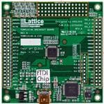
Connectors are provided for key functions and test points on this evaluation board, as shown in Figure 1. The USB
programming cable is connected to the USB port (J2) shown on the bottom of the figure.
Access to the ispPOWR1014A device’s I/O pins are available as shown along the right and left edges of the
assembly, where two 2x20 blocks of pads (J3 and J6) support the attachment of test probes or a ribbon-cable connector. An array of 60 prototype holes for interfacing is shown at the top of the figure.
Several LEDs on the evaluation board are provided to indicate proper function and as aids to debugging. The green
LED (D9) indicates that the on-board 3.3V supply (derived from the input USB voltage) is powered up. Eight red
LEDs (D1 through D8) are provided to demonstrate control of digital outputs OUT7 through OUT14 so that a user
may easily view the progress of Sequence, Monitor, Reset programs run on the evaluation board.
2
�POWR1014A Breakout Board
Evaluation Kit User’s Guide
Figure 1. POWR1014A Breakout Board, Top Side
LED Array
4x15 Prototype Area
20-Pin Header
(J3)
20-Pin Header
(J6)
USB Interface
(J2)
JTAG Header Landing
(J1)
Storage and Handling
Static electricity can shorten the lifespan of electronic components. Please observe these tips to prevent damage
that could occur from electro-static discharge:
• Use anti-static precautions such as operating on an anti-static mat and wearing an anti-static wrist-band.
• Store the evaluation board in the packaging provided.
• Touch a metal USB housing to equalize voltage potential between you and the board.
Software Requirements
The POWR1014A Breakout Board uses an FTDI USB interface device that requires USB drivers contained in the
following software to communicate properly. Initial manual testing (Quick Start) using the computer USB power
maybe accomplished before loading the software drivers. For manual testing only, plug the board into the computer
USB port and “cancel” when requested to install new hardware. If the incorrect drivers are installed by Windows
they may require removal before the FTDI USB drivers can be loaded and the POWR1014A Breakout Board can
be recognized by the computer.
• PAC-Designer design software
• ispVM™ System device programming software
• FTDI USB drivers
3
�POWR1014A Breakout Board
Evaluation Kit User’s Guide
POWR1014A Device
This board features the Power Manager II ispPAC-POWR1014A general-purpose power-supply monitor and
sequence controller, incorporating both in-system programmable logic and in-system programmable analog functions implemented in non-volatile E2CMOS technology. A complete description of this device can be found in the
ispPAC-POWR1014/A Data Sheet.
Demonstration Design
Lattice provides a pre-programmed demo to illustrate basic operation of the POWR1014A device. The program
demonstrates sequencing of the output pins Out4 through Out14. Using an internal timer the program alternates
the POWR1014A outputs, illuminating LEDs D1, D3, D5 and D7 then LEDs D2, D4, D6 and D8.
Note: To restore the factory default demo or program it with other Lattice-supplied examples see the Download
Demo or Create New Designs section of this document.
Run the Demonstration Design
USB Cable Power Connection
Download USB Hardware Drivers: Communication with the POWR1014A Breakout Board with a PC via the USB
cable will require the USB hardware drivers contained in the Software Requirements section. Loading these drivers
enables the computer to recognize and program the POWR1014A Breakout Board. To load these USB drivers, use
one of the following methods:
Preferred Installation:
1. Run ispVM System and choose Install/Uninstall LSC USB/Parallel Port Driver from the ispTools tab.
Optional Installation:
1. Connect the USB cable from a USB port on your PC to the board’s USB mini-B socket (J2). After connection is
made, a green Power LED (D9) will light up indicating the board is powered on.
2. If you are prompted, “Windows may connect to Windows Update” select No, not this time from available
options and click Next to proceed with the installation. Choose the Install from specific location (Advanced)
option and click Next.
3. Browse to the FTDI USB Drivers listed in the Software Requirements section. Search for the best driver in
these locations and click the Browse button to browse to the Windows driver folder created in the Download
Windows USB Hardware Drivers section. Select the CDM 2.04.06 WHQL Certified folder and click OK.
4. Click Next. A screen will display as Windows copies the required driver files. Windows will display a message
indicating that the installation was successful.
5. Click Finish to install the USB driver.
Reprogramming Designs
The support demo is preprogrammed into the POWR1014A. It may be desirable to reload the original demo program after any design modification. Lattice distributes the source (JED) and schematic (PAC) files for demonstration designs compatible with the POWR1014A Breakout Board.
Refreshing the programming for U4 POWR1014A will require the demo JEDEC file. This is available directly as a
.jed file or can be compiled from the .pac files using PAC-Designer. The .jed files are then loaded into U4 via the
USB cable using ispVM software.
Programming Devices with ispVM
To restore a POWR1014A Breakout Board to factory settings or load an alternative demo design, use the procedures in this section.
4
�POWR1014A Breakout Board
Evaluation Kit User’s Guide
For more information see AN6062, Using ispVM System to Program ispPAC Devices.
1. Connect the board to a host PC using the USB port or JTAG header connection.
2. Follow the USB Cable Interface procedure below to program the evaluation board.
USB Cable Interface Connection: The POWR1014A Breakout Board is equipped with a built-in USB-based programming circuit. This consists of a USB PHY and a USB connector. When the board is connected to a PC with a
USB cable, it is recognized by the ispVM System software as a “USB Download Cable”. The POWR1014A can
then be scanned and programmed using the ispVM System software.
Download Demo or Create New Designs
1. Browse to the POWR1014A Breakout Board design files.
2. Extract the contents of PAC_POWR1014A_BREAKOUTBOARD.zip to an accessible location on your hard
drive.
The demo design directory (PAC_POWR1014A_BREAKOUTBOARD) is unpacked.
Demo
Directory
PAC_POWR1014A_BLINKER
PAC_POWER1014A_BLINKER.JED
PAC_POWR1014A_BREAKOUTBOARD
Create or Modify the .jed Design by compiling a PAC-Designer using .PAC file: Use the procedure
below to recompile the demo project for the POWR1014A Breakout Board or modify for a custom design.
1. Run PAC-Designer.
2. From the File tab open either the .PAC project file from the Download Demo Designs section or other
>.PAC file if implementing a custom design.
3. Modification of the I/Os or change of sequencing for custom designs can be done at this step.
4. From the schematic block diagram, double-click the Sequence Controller block. The LogiBuilder interface
appears.
Table 1. Demo Design Sequencing Program (for Reference Only)
Step
Instruction
Outputs
Int.
Comment
0
Begin Startup Sequence
0
POWR1014A reset
OUT4 = 1, OUT5 = 0, OUT6 = 1,
OUT7 = 0, OUT8 = 0, OUT9 = 0,
OUT14 = 0,
0
Initializes outputs
1
0
Set outputs 4 through 14,
0 = Hi Z, 1 = Ground, then
waits for power good
0
3
OUT4 = 1, OUT5 = 0, OUT6 = 1,
OUT7 = 0, OUT8 = 1, OUT9 = 0,
OUT10 = 1, OUT11 = 0, OUT12 = 1,
OUT13 = 0, OUT14 = 1,
Alternate output settings for
OUT4 throughOUT14
4
Wait for 524.29ms using timer 1
0
Wait 0.5 sec
OUT3 = 1, OUT4 = 0, OUT5 = 1,
OUT6 = 0, OUT7 = 1, OUT8 = 0,
OUT9 = 1, OUT10 = 0, OUT11 = 1,
OUT12 = 0, OUT13 = 1, OUT14 = 0,
0
5
Alternate outputs OUT4
through OUT14
6
Wait for 524.29ms using Timer 1
0
Wait 0.5 sec
Wait for AGOOD
2
OUT4 = 0, OUT5 = 1, OUT6 = 0,
OUT7 = 1, OUT8 = 0, OUT9 = 1,
OUT10 = 0, OUT11 = 1, OUT12 = 0,
OUT13 = 1, OUT14 = 0,
5
�POWR1014A Breakout Board
Evaluation Kit User’s Guide
Table 1. Demo Design Sequencing Program (for Reference Only)
Step
Instruction
Outputs
Int.
Comment
Go to Step 3
0
Enter loop to alter sequence of
OUT4 through OUT14.
Flashes odd then even LEDs.
8
Begin shut-down sequence
0
9
Halt (end-of-program)
0
7
5. Choose Tools > Compile LogiBuilder Design. After a few moments the JEDEC programming file is output.
Click OK.
6. From the toolbar launch JED to download and save the file.
Note: PAC-Designer may not recognize files that have certain characters such as spaces or periods in the directory
path.
To program the device using a .jed file:
1. From the Start menu run ispVM System.
ispVM appears.
2. Choose Options > Cable and I/O Port Setup...
The Cable and I/O Port Setup dialog appears.
3. Make the following selections:
Cable Type: USB2
Port Setting: FTUSB-0
Click OK.
4. Choose ispTools > Scan Chain.
The New Scan Configuration Setup window appears. The POWR1014A appears in the device list.
5. Highlight the POWR1014A, right-click and choose Edit Device...
The Device Information dialog appears.
6. From the Set Device Operations section, click the Browse button.
The Open Data File dialog appears.
7. Download the .jed file either downloaded from the Lattice web site or file compiled using PAC-Designer by
browsing to the \project folder, selecting .jed, and clicking OK.
8. Select the device to be programmed by highlighting and then right-clicking and choose Set Device Operations. From the Operation list choose Flash Erase, Program, Verify.
9. From the toolbar select Go to program device
Programming requires about 20-40 seconds. A small timer window will appear to show elapsed programming time.
At the end of programming, the configuration setup window should show a “PASS” in the Status column.
6
�POWR1014A Breakout Board
Evaluation Kit User’s Guide
POWR1014A Breakout Board
This section describes the features of the ispPOWR1014A Breakout board detail.
POWR1014A
The ispPAC-POWR1014A-02TN48I in the 7x7mm 48-pin TQFP package has the ability to monitor 10 analog inputs
and provides 14 digital outputs. Two of the outputs can be configured to provide 6V to 12V MOSFET gate drive.
Table 2. POWR1014A Interface Reference
Item
Description
Reference designator
U4
Part number
POWR1014A
Manufacturer
Lattice Semiconductor
Web site
www.latticesemi.com
JTAG Interface Circuits
For power and programming, a FTDI USB UART/FIFO IC converter provides a communication interface between a
PC host and the JTAG programming chain of the POWR1014A Breakout Board. The USB 5V supply is also used
as a source for the 3.3V supply rail. A USB mini-B socket is provided for the USB connector cable.
Table 3. JTAG Interface Reference
Item
Description
Reference designator
U2
Part number
FT2232H
Manufacturer
Future Technology Devices International (FTDI)
Web site
www.ftdichip.com
Table 4. JTAG Programming Pin Information
Description
POWR1014A Pin
Test Data Output
Pin 21 TDO
Test Data Output
—
Test Data Input
Pin 18 TDI
Test Mode Select
Pin 16 TMS
Test Clock
Pin 22 TCK
LEDs
A green LED (D9) is used to indicate USB 5V power and red LEDs (D1 to D8) are used to show the status of the
outputs.
Table 5. User LEDs Reference
Item
Description
Reference designators
D1 through D9
Part number
LTST-C190KGKT and LTST-C190KRKT
Manufacturer
Lite-On It Corporation
Web site
www.liteonit.com
7
�POWR1014A Breakout Board
Evaluation Kit User’s Guide
Power Supply
3.3V supply rail is converted from the USB 5V interface by a linear regulator U1 when the board is connected to a
host PC.
Test Points
The ability to program the POWR1014A without enabling the device I/Os can be accomplished by powering the
VCCPROG only. After programming, VCCPROG should be left open and VCCA and VCCD should be powered for
normal operation. TP1 provides access to VCCPROG. See Appendix A. Schematics for more details:
• TP1, VCCPROG
USB Programming and Debug Interface
The USB mini-B socket of the POWR1014A Breakout Board serves as the programming and debug interface.
JTAG Programming
For JTAG programming a preprogrammed USB PHY peripheral controller is provided on the board to serve as the
programming interface to the POWR1014A.
Programming requires ispVM System software.
Mechanical Specifications
Dimensions: 3 in. [L] x 3 in. [W] x 1/2 in. [H]
Environmental Requirements
The POWR1014A Breakout Board must be stored between -40° C and 100° C. The recommended operating temperature is between 0° C and 90° C.
The board can be damaged without proper anti-static handling.
Glossary
LED: Light Emitting Diode.
RoHS: Restriction of Hazardous Substances Directive.
USB: Universal Serial Bus.
FTDI: Future Technology Devices International Ltd.
Troubleshooting
Use the tips in this section to diagnose problems with the POWR1014A Breakout Board.
LEDs Do Not Flash
If power is applied (LED D9 illuminated) but LEDs D1 through D8 do not flash according to the preprogrammed
counter demonstration then it is likely the board has been reprogrammed with a new design. Follow the directions
in the Demonstration Design section to restore the factory default.
USB Cable Not Detected
If ispVM System cannot detect the USB2 cable type programming interface to the board, the incorrect USB driver
may have been installed. This usually occurs if you attach the board to your PC prior to installing the USB driver or
ispVM System software.
8
�POWR1014A Breakout Board
Evaluation Kit User’s Guide
To correct a USB driver installation:
1. Start ispVM and choose Options > Cable and I/O Port Setup.
The Cable and I/O Port Setup Dialog appears.
2. Click the Troubleshooting the USB Driver Installation Guide link.
The Troubleshooting the USB Driver Installation Guide document appears in your system’s PDF file reader.
3. Follow the instructions in the guide to install the Lattice USB driver.
Determine the Source of a Pre-Programmed Device
You may receive your POWR1014A Breakout board after it has been reprogrammed by someone else. To restore
the board to the factory default, see the Download Demo or Create New Designs section for details on downloading
and reprogramming the device.
You can also determine which demo design is currently programmed onto the board by comparing the JEDEC
checksums against of the programming file with what is read from the programmed device.
To compare JEDEC file checksum:
1. Connect the POWR1014A Breakout Board to a host PC using the USB port.
2. Start ispVM and choose ispTools > Scan.
The device appears in the Device List.
3. Double-click the device row.
The Device Information dialog appears.
4. Click the Browse button.
The Save as Data File dialog appears.
5. Specify a new JEDEC Data File name and click the Save button.
6. From the Operation list choose Read and Save JEDEC and click OK.
7. Choose Project > Download.
ispVM reads the contents from the device and writes the results to the JEDEC file specified.
Open the JEDEC file into a text editor and page to the bottom of the file.
Note the hexadecimal checksum at the line above the User Electronic Data note line. Compare this value
against the checksum of the original JEDEC demo programming files.
Ordering Information
Description
POWR1014A Breakout Board Evaluation Kit
Ordering Part Number
POWR1014A-B-EVN
Technical Support Assistance
Hotline: 1-800-LATTICE (North America)
+1-503-268-8001 (Outside North America)
e-mail: techsupport@latticesemi.com
Internet: www.latticesemi.com
9
China RoHS Environment-Friendly
Use Period (EFUP)
�POWR1014A Breakout Board
Evaluation Kit User’s Guide
Revision History
Date
Version
March 2011
01.0
Initial release.
Change Summary
February 2012
01.1
Updated document with new corporate logo.
© 2012 Lattice Semiconductor Corp. All Lattice trademarks, registered trademarks, patents, and disclaimers are as
listed at www.latticesemi.com/legal. All other brand or product names are trademarks or registered trademarks of
their respective holders. The specifications and information herein are subject to change without notice.
10
�11
A
B
C
D
5
5
4
4
PROTOTYPE AREA
LED ARRAY
2
3
2
Resistant Tolerance: R12 1%
All the rest up to 5%
CONNECTED HEADER
isp POWR
CONNECTED HEADER
3
Date:
Size
B
Title
AXELSYS
Sunday, December 19, 2010
POWR1014A-B-EVN
Document Number
1
Sheet
1
POWR1014A Breakout Board, Cover
1
of
4
Rev
A
A
B
C
D
POWR1014A Breakout Board
Evaluation Kit User’s Guide
Appendix A. Schematics
Figure 2. POWR1014A Breakout Board
USB to JTAG
USB CON
�A
B
C
5
1
2
J2
2
VCC
DD+
ID
GND
1k
SKT_MINIUSB_B_RA
D9
Green
R1
1
1
C10
10u
1
2
3
4
5
VBUS_5V
2
IN
2
FT_EEDATA
1
0
1
0.1uF
R19
2
C20
600ohm 500mA
L4
3
OUT
TAB
R22
1
R21
10k
1
10
0
C15
0.1uF
2k2
2
2
R17 2
R18
1 NCP1117ST33
GND
2
4
FT_EECS
FT_EECLK
R2
2
Default
1
0
1
C11
22u
4
Dm
Dp
2
1
2
3
4
VCC
NU
ORG
VSS
93LC56-SO8
CS
CLK
DI
DO
U3
C13
0.1uF
8
7
6
5
1
C21
0.1uF
C12
4u7
VCC3FT
VCC3FT
L3
2
1
600ohm 500mA
L2
2
1
600ohm 500mA
C1
4u7
C14
0.1uF
C2
0.1uF
VCC3D
1
C3
4u7
C18
18pF
C16
10u
VCC1_8FT
2
1
2
1
12MHZ
3
3
4
3
VCC3FT
G1 G2
1
X1
C4
0.1uF
C17
0.1uF
2
VCC3A
C19
18pF
63
62
61
FT_EECS
FT_EECLK
FT_EEDATA
13
3
2
6
12k 1%
2
R12
1
14
2
R11
5k1
1
7
8
49
50
VCC1_8FT
FT2232H
VCC3FT
PWREN#
BCBUS0
BCBUS1
BCBUS2
BCBUS3
BCBUS4
BCBUS5
BCBUS6
BCBUS7
BDBUS0
BDBUS1
BDBUS2
BDBUS3
BDBUS4
BDBUS5
BDBUS6
BDBUS7
ACBUS0
ACBUS1
ACBUS2
ACBUS3
ACBUS4
ACBUS5
ACBUS6
ACBUS7
ADBUS0
ADBUS1
ADBUS2
ADBUS3
ADBUS4
ADBUS5
ADBUS6
ADBUS7
SUSPEND#
FTDI High-Speed USB
TEST
OSCO
OSCI
EECS
EECLK
EEDATA
REF
RESET#
DM
DP
VREGOUT
VREGIN
U2
FT2232HL
VCC3FT
2
36
60
48
52
53
54
55
57
58
59
38
39
40
41
43
44
45
46
26
27
28
29
30
32
33
34
16
17
18
19
21
22
23
24
VCC3FT
1
2
L1
2
1
600ohm 500mA
2
1
10
10
10
0
C5
0.1uF
cc0402
1
2
R3 2
R4 2
R7 2
R9
2
3
C6
0.1uF
cc0402
1
2
U1
1
2
1
2
1
2
3
4
5
6
7
8
TCK
TDO
TDI
TMS
DNI
Date:
Size
C
Title
header_1x8
1
2
3
4
5
6
7
8
J1
C7
0.1uF
cc0402
1
2
2
1
2
1
2
1
2
VCC_3.3V
1
2
1
2
1
2
R15
5k1
R20
5k1
R16
5k1
VCC3FT
C9
0.1uF
cc0402
1
TCK ( 4 )
TDI ( 4 )
TDO ( 4 )
TMS ( 4 )
TDISEL ( 4 )
ATDI ( 4 )
1
Tuesday, December 21, 2010
POWR1014A-B-EVN
Document Number
Sheet
2
of
POWR1014A Breakout Board, USBIF to JTAG
AXELSYS
R14
5k1
TCK
TDI
TDO
TMS
VCC3FT
C8
0.1uF
cc0402
1
2
VBUS_5V
1
2
2
1
4
9
VPHY
VPLL
4
1
2
2
1
12
37
64
VCORE
VCORE
VCORE
AGND
1
2
20
31
42
56
10
1
2
VCCIO
VCCIO
VCCIO
VCCIO
GND
GND
GND
GND
GND
GND
GND
GND
1
5
11
15
25
35
47
51
1
2
1
12
2
D
5
4
Rev
A
A
B
C
D
POWR1014A Breakout Board
Evaluation Kit User’s Guide
Figure 3. USB Interface to JTAG
�A
B
C
5
J4
Proto Type Area
Proto Type Area
( 4 ) OUT[14:4]
4X15 PROTOTYPE AREA
1
VCC3D
1
2
1
OUT14 2
D8
Red
R39
2k
1
2
R51
2k
1
2
1
OUT13 2
4
R52
2k
D6
Red
R41
2k
R53
2k
VCC3D
D5
Red
R42
2k
OUT6
OUT5
OUT4
R54
2k
D4
Red
R43
2k
R59
2k
1
2
1
2
SMBA_OUT
LED DISPLAY ARRAY
D7
Red
R40
2k
4
1
2
1
2
1
OUT12 2
1
2
1
2
1
OUT11 2
1
2
1
2
R55
2k
R60
2k
1
R61
2k
D3
Red
R44
2k
2
R56
2k
R62
2k
3
D2
Red
R45
2k
R57
2k
( 4 ) SCL_
( 4 ) SDA_
3
2
1
2
1
2
1
2
OUT9
1
OUT10 2
1
2
1
2
2
OUT8
1
1
2
OUT7
1
1
2
1
2
2
1
D1
Red
R58
2k
( 4 ) HVOUT2
( 4 ) HVOUT1
(4)
(4)
(4)
(4)
ispIN1
ispIN2
ispIN3
ispIN4
C27
0.1uF
( 4 ) SMBA_OUT
( 4 ) VMON[10:1]
R46
2k
2k2
R26
( 4 ) PLDCLK
( 4 ) MCLK
( 4 ) RESETB
2k2
R25
VCC3D
2
1
( 4 ) OUT[14:4]
1
2
1
2
1
2
13
C28
0.1uF
1
2
D
5
VMON10
VMON9
VMON8
VMON7
VMON6
VMON5
VMON4
VMON3
VMON2
VMON1
C29
0.1uF
VCC_3.3V
OUT14
OUT13
OUT12
OUT11
OUT10
OUT9
OUT8
OUT7
OUT6
OUT5
OUT4
J3
1 2
3 4
5 6
7 8
9 10
1112
1314
1516
1718
1920
2122
2324
2526
2728
2930
3132
3334
3536
3738
3940
2
4
6
8
10
12
14
16
18
20
22
24
26
28
30
32
34
36
38
40
2
J6
1 2
3 4
5 6
7 8
9 10
1112
1314
1516
1718
1920
2122
2324
2526
2728
2930
3132
3334
3536
3738
3940
2
4
6
8
10
12
14
16
18
20
22
24
26
28
30
32
34
36
38
40
header_2x20
DNI
1
3
5
7
9
11
13
15
17
19
21
23
25
27
29
31
33
35
37
39
EXTERNAL POWER PINS
header_2x20
DNI
1
3
5
7
9
11
13
15
17
19
21
23
25
27
29
31
33
35
37
39
2
Title
Date:
Size
C
AXELSYS
1
Tuesday, December 21, 2010
POWR1014A-B-EVN
Document Number
Sheet
3
of
POWR1014A Breakout Board, CON and LED
1
4
Re v
A
A
B
C
D
POWR1014A Breakout Board
Evaluation Kit User’s Guide
Figure 4. Connectors and LEDs
�A
B
5
( 3 ) ispIN1
( 3 ) ispIN2
( 3 ) ispIN3
( 3 ) ispIN4
4
R47
5k1
R48
5k1
R49
5k1
R50
5k1
( 3 ) VMON[10:1]
1
C
4
1
2
1
2
1
2
14
2
TDISEL
ATDI
TDI
TMS
TCK
TDO
( 3 ) SCL_
( 3 ) SDA_
(2)
(2)
(2)
(2)
(2)
(2)
VMON1
VMON2
VMON3
VMON4
VMON5
VMON6
VMON7
VMON8
VMON9
VMON10
3
3
39
38
19
17
18
16
22
21
44
46
47
48
25
26
27
28
32
33
34
35
36
37
ispPAC-POWR1014A-02TN48I
SCL
SDA
TDISEL
ATDI
TDI
TMS
TCK
TDO
IN1
IN2
IN3
IN4
VMON1
VMON2
VMON3
VMON4
VMON5
VMON6
VMON7
VMON8
VMON9
VMON10
U4
VCC3A
VCC3D
HVOUT1
HVOUT2
C22
0.1uF
cc0402
GNDA
GNDD2
GNDD1
PLDCLK
MCLK
RESETB
SMBA_OUT3
OUT4
OUT5
OUT6
OUT7
OUT8
OUT9
OUT10
OUT11
OUT12
OUT13
OUT14
TP1
2
1
VCC3A
1
23
41
29
45
24
20
VCCD1
VCCD2
VCCA
VCCINP
VCCPROG
VCCJ
15
14
30
31
7
42
43
40
13
12
11
10
9
8
6
5
4
3
2
1
VCC3D
1
C23
0.1uF
cc0402
OUT4
OUT5
OUT6
OUT7
OUT8
OUT9
OUT10
OUT11
OUT12
OUT13
OUT14
2
1
2
C24
0.1uF
cc0402
HVOUT1 ( 3 )
HVOUT2 ( 3 )
C25
0.1uF
cc0402
2
C26
0.1uF
cc0402
PLDCLK ( 3 )
MCLK ( 3 )
RESETB ( 3 )
OUT[14:4] ( 3 )
SMBA_OUT ( 3 )
2
1
2
1
2
D
5
Title
Date:
Size
C
AXELSYS
1
Sunday, December 19, 2010
POWR1014A-B-EVN
Document Number
Sheet
4
of
4
POWR1014A Breakout Board, Lattice ispPOWR
1
Re v
A
A
B
C
D
POWR1014A Breakout Board
Evaluation Kit User’s Guide
Figure 5. POWR1014A
�POWR1014A Breakout Board
Evaluation Kit User’s Guide
Appendix B. Bill of Materials
Table 6. POWR1014A Breakout Board Evaluation Kit Bill of Materials
Item
Quantity
Reference
1
3
C1, C3, C12
2
21
C2, C4, C5, C6,
C7, C8, C9, C13
Part
Class
Description
Manufacturer
Manufacturer
Part Number
Digikey P/N
PCB
Footprint
4u7
Cap Cer 4.7uF
Discrete 6.3V 10% X5R
0603
Panasonic
ECJ-1VB0J475K
0.1uF
Cer 0.1uF
Discrete Cap
16V X7R 0402
Kemet
C0402C104K4RA 399-3521-2-ND
CTU
cc0402
PCC2396CT-ND
Assembly
cc0603
C14, C15, C17,
C20, C21, C22
C23, C24, C25,
C26, C27, C28
C29
3
2
C10, C16
10u
Cap Cer 10uF
Discrete 6.3V 20% X5R
0603
Panasonic
ECJ-1VB0J106M
cc0603
4
1
C11
22u
CER 22UF
Discrete CAP
10V X5R 0805
Taiyo Yuden
LMK212BJ226M
G-T
cc0805
5
2
C18, C19
18pF
CER 18PF
Discrete CAP
25V C0G 0402
Kemet
C0402C180K3GA C0402C180K3GA
CTU
CTU-ND
cc0402
6
8
D1, D2, D3, D4,
D5, D6, D7, D8
Red
LED SUPER RED
Discrete CLEAR 0603
Lite-On Inc
SMD
LTST-C190KRKT
7
1
D9
Green
LED SUPER
Discrete GREEN CLEAR
0603 SMD
LTST-C190KGKT
8
1
J1
header_1x8
9
1
J2
SKT_MINIUSB_B_RA
10
2
J3, J6
11
1
J4
Lite-On Inc
160-1436-2-ND
led_0603
led_0603
hdr_amp_87220_
8_1x8_100
IO
Neltron
5075BMR-05-SMCR
skt_miniusb_b_ra
header_2x20
Proto Type Area
hdr_samtec_mtsw
_2x20_100
DNI
hdr_th_4x15_100
DNI
600ohm 500mA
Ferrite Bead
Discrete 600ohm@100MH Murata
z 500mA 0603
BLM18AG601SN
1D
490-1014-1-ND
FB0603
12
4
L1, L2, L3, L4
13
1
R1
1k
1/16W 1K 1% Yageo
Discrete Res
0402
RC0402FR071KL
311-1.00KLRTRND
cr0402
14
8
R2, R3, R4, R7,
R9, R17, R18
0
1/10W 0.0
Discrete Res
Ohm 5% 0603
Yageo
RC0603JR070RL
311-0.0GRTR-ND
cr0603
5k1
1/16W 5.1K
Discrete Res
1% 0402
Yageo
RC0402FR075K1L
311-5.10KLRTRND
cr0402
12k
1/16W 12.0K Yageo
Discrete Res
1% 0402
RC0402FR0712KL
311-12.0KLRTRND
cr0402
10k
1/16W 10.0K Yageo
Discrete Res
1% 0402
RC0402FR0710KL
311-10.0KLRTRND
cr0402
Yageo
RC0402FR072K2L
311-2.20KLRTRND
cr0402
Yageo
RC0402JR072KL
311-2.0KJRTRND
cr0402
R19
15
9
R11, R14, R15,
R16, R20, R47
R48, R49, R50
16
17
1
1
R12
R21
18
3
R22, R25, R26
2k2
1/16W 2.2K
Discrete Res
1% 0402
19
20
R39, R40, R41,
R42, R43, R44
2k
RES 2.0K OHM
Discrete 1/16W 5% 0402
SMD
R45, R46, R51,
R52, R53, R54,
R55, R56, R57,
R58, R59, R60
R61, R62
20
1
TP1
TP_S_40_63
21
1
U1
NCP1117ST33
22
1
U2
FT2232HL
23
1
U3
93LC56-SO8
24
1
U4
ispPAC-POWR1014A
-02TN48I
25
1
X1
12MHZ
IO
Square test point,
40mil inner diameter, 63mil outer
diameter
tp_s_40_63
On Semi
IC
IC 93LC56
EEPROM
sot223_4p
FTDI
FT2232HL
Microchip
93LC56T-I/SN
tqfp64_0p5_12p2
x12p2_h1p6
so8_50_244
tqfp48_0p5_9p2x
9p2_h1p7
TXC
15
7M-12.000MAAJT
DNI
crystal_4p_3p2x2
p5
�


 工商网监
湘ICP备2023018690号
工商网监
湘ICP备2023018690号
