SiI9136-3/SiI1136 HDMI Deep Color
Transmitter
Data Sheet
SiI-DS-1084-D
June 2017
�SiI9136-3/SiI1136 HDMI Deep Color Transmitter
Data Sheet
Contents
Acronyms in This Document ................................................................................................................................................. 6
1. General Description ...................................................................................................................................................... 7
1.1. Video Input ........................................................................................................................................................... 7
1.2. Audio Input ........................................................................................................................................................... 7
1.3. HDMI Output ........................................................................................................................................................ 7
1.4. Control Capability ................................................................................................................................................. 7
1.5. Packaging .............................................................................................................................................................. 7
2. Product Family .............................................................................................................................................................. 8
3. Functional Description .................................................................................................................................................. 9
3.1. Video Data Input and Conversion ......................................................................................................................... 9
3.1.1.
Input Clock Multiplier/Divider .................................................................................................................... 10
3.1.2.
Video Data Capture ..................................................................................................................................... 10
3.1.3.
Embedded Sync Decoder ............................................................................................................................ 10
3.1.4.
Data Enable Generator ............................................................................................................................... 10
3.1.5.
Combiner .................................................................................................................................................... 10
3.1.6.
4:2:2 to 4:4:4 Upsampler ............................................................................................................................ 10
3.1.7.
RGB Range Expansion ................................................................................................................................. 10
3.1.8.
Color Space Converter ................................................................................................................................ 11
3.1.9.
RGB/YCbCr Range Compression ................................................................................................................. 11
3.1.10. 4:4:4 to 4:2:2 Downsampler ....................................................................................................................... 11
3.1.11. Clipping ....................................................................................................................................................... 11
3.1.12. 18-to-8/10/12/16-Dither ............................................................................................................................ 11
3.2. Audio Data Capture............................................................................................................................................. 11
3.3. Framer ................................................................................................................................................................. 11
3.4. HDCP Encryption Engine/XOR Mask ................................................................................................................... 11
3.5. HDCP Key ROM ................................................................................................................................................... 12
3.6. TMDS Transmitter ............................................................................................................................................... 12
3.7. GPIO .................................................................................................................................................................... 12
3.8. Hot Plug Detector ............................................................................................................................................... 12
3.9. CEC Interface ....................................................................................................................................................... 12
3.10.
DDC Master I2C Interface ................................................................................................................................ 12
3.11.
Receiver Sense and Interrupt Logic ................................................................................................................ 13
3.12.
Configuration Logic and Registers .................................................................................................................. 13
3.13.
I2C Slave Interface ........................................................................................................................................... 13
4. Electrical Specifications .............................................................................................................................................. 14
4.1. Absolute Maximum Conditions .......................................................................................................................... 14
4.2. Normal Operating Conditions ............................................................................................................................. 14
4.2.1.
I/O Specifications ........................................................................................................................................ 15
4.2.2.
DC Power Supply Specifications .................................................................................................................. 16
4.3. AC Specifications ................................................................................................................................................. 16
4.3.1.
Video/HDMI Timing Specifications ............................................................................................................. 16
4.3.2.
Audio AC Timing Specifications ................................................................................................................... 17
4.3.3.
Video AC Timing Specifications ................................................................................................................... 18
4.3.4.
Control Signal Timing Specifications ........................................................................................................... 18
4.3.5.
CEC Timing Specifications ........................................................................................................................... 19
4.4. Timing Diagrams ................................................................................................................................................. 19
4.4.1.
Input Timing Diagrams ................................................................................................................................ 19
4.4.2.
Reset Timing Diagrams ............................................................................................................................... 20
4.4.3.
TMDS Timing Diagram ................................................................................................................................ 20
4.4.4.
Audio Timing Diagrams ............................................................................................................................... 21
4.4.5.
I2C Timing Diagrams .................................................................................................................................... 21
5. Pin Diagram and Descriptions ..................................................................................................................................... 22
© 2010-2017 Lattice Semiconductor Corp. All Lattice trademarks, registered trademarks, patents, and disclaimers are as listed at www.latticesemi.com/legal. All other brand or product names are
trademarks or registered trademarks of their respective holders. The specifications and information herein are subject to change without notice.
2
SiI-DS-1084-D
�SiI9136-3/SiI1136 HDMI Deep Color Transmitter
Data Sheet
5.1. Pin Diagram......................................................................................................................................................... 22
5.2. Pin Descriptions .................................................................................................................................................. 23
5.2.1.
Video Data Input ......................................................................................................................................... 23
5.2.2.
TMDS Output .............................................................................................................................................. 24
5.2.3.
Audio Input ................................................................................................................................................. 24
5.2.4.
DDC, CEC, Configuration, and Control ........................................................................................................ 25
5.2.5.
Power and Ground ...................................................................................................................................... 25
5.2.6.
Not Connected and Reserved ..................................................................................................................... 25
6. Feature Information ................................................................................................................................................... 26
6.1. RGB to YCbCr Color Space Converter.................................................................................................................. 26
6.2. YCbCr to RGB Color Space Converter.................................................................................................................. 26
6.3. I2C Register Information ..................................................................................................................................... 27
6.4. I2S Audio Input .................................................................................................................................................... 27
6.5. Direct Stream Digital Input ................................................................................................................................. 27
6.6. S/PDIF Input ........................................................................................................................................................ 27
6.7. I2S and S/PDIF Supported MCLK Frequencies ..................................................................................................... 27
6.8. Audio Downsampler Limitations......................................................................................................................... 28
6.9. High Bitrate Audio on HDMI ............................................................................................................................... 29
6.10.
Power Domains ............................................................................................................................................... 29
6.11.
Internal DDC Master ....................................................................................................................................... 30
6.12.
Deep Color Support ........................................................................................................................................ 30
6.13.
Source Termination ........................................................................................................................................ 31
6.14.
3D and 4K Video Formats ............................................................................................................................... 31
6.15.
Control Signal Connections ............................................................................................................................. 32
6.16.
Input Data Bus Mapping ................................................................................................................................. 33
6.16.1. Common Video Input Formats .................................................................................................................... 33
6.16.2. RGB and YCbCr 4:4:4 Separate Sync ........................................................................................................... 34
6.16.3. YC 4:2:2 Separate Sync Formats ................................................................................................................. 36
6.16.4. YC 4:2:2 Embedded Syncs Formats ............................................................................................................. 38
6.16.5. YC Mux 4:2:2 Separate Sync Formats ......................................................................................................... 40
6.16.6. YC Mux 4:2:2 Embedded Sync Formats ...................................................................................................... 42
6.16.7. RGB and YCbCr 4:4:4 Dual Edge Mode Formats ......................................................................................... 44
7. Design Recommendations .......................................................................................................................................... 47
7.1. Power Supply Decoupling ................................................................................................................................... 47
7.2. Power Supply Sequencing ................................................................................................................................... 47
7.3. ESD Recommendations ....................................................................................................................................... 47
7.4. High-Speed TMDS Signals ................................................................................................................................... 48
7.4.1.
Layout Guidelines ....................................................................................................................................... 48
7.4.2.
TMDS Output Recommendation ................................................................................................................ 48
7.4.3.
EMI Considerations ..................................................................................................................................... 48
8. Packaging .................................................................................................................................................................... 49
8.1. ePad Requirements............................................................................................................................................. 49
8.2. PCB Layout Guidelines ........................................................................................................................................ 49
8.3. Package Dimensions ........................................................................................................................................... 50
8.4. Marking Specification ......................................................................................................................................... 51
8.5. Ordering Information .......................................................................................................................................... 51
References .......................................................................................................................................................................... 52
Standards Documents..................................................................................................................................................... 52
Standards Groups ........................................................................................................................................................... 52
Lattice Semiconductor Documents ................................................................................................................................. 52
Technical Support ........................................................................................................................................................... 53
Revision History .................................................................................................................................................................. 54
© 2010-2017 Lattice Semiconductor Corp. All Lattice trademarks, registered trademarks, patents, and disclaimers are as listed at www.latticesemi.com/legal. All other brand or product names are
trademarks or registered trademarks of their respective holders. The specifications and information herein are subject to change without notice.
SiI-DS-1084-D
3
�SiI9136-3/SiI1136 HDMI Deep Color Transmitter
Data Sheet
Figures
Figure 1.1. Typical Application for Streaming Sticks ............................................................................................................. 7
Figure 3.1. SiI9136-3/SiI1136 Functional Block Diagram ...................................................................................................... 9
Figure 3.2. Transmitter Video Data Processing Path ............................................................................................................ 9
Figure 4.1. VCCTP Test Point for VCC Noise Tolerance ....................................................................................................... 14
Figure 4.2. IDCK Clock Duty Cycle ....................................................................................................................................... 19
Figure 4.3. Control and Data Single-Edge Setup and Hold Times—EDGE = 1 ..................................................................... 19
Figure 4.4. Control and Data Single-Edge Setup and Hold Times—EDGE = 0 ..................................................................... 19
Figure 4.5. Control and Data Dual-Edge Setup and Hold Times ......................................................................................... 19
Figure 4.6. VSYNC and HSYNC Delay Times Based on DE ................................................................................................... 20
Figure 4.7. DE HIGH and LOW Times .................................................................................................................................. 20
Figure 4.8. Conditions for Use of RESET# ............................................................................................................................ 20
Figure 4.9. RESET# Minimum Timings................................................................................................................................. 20
Figure 4.10. Differential Transition Times .......................................................................................................................... 20
Figure 4.11. I2S Input Timings ............................................................................................................................................. 21
Figure 4.12. S/PDIF Input Timings ....................................................................................................................................... 21
Figure 4.13. MCLK Timings .................................................................................................................................................. 21
Figure 4.14. DSD Input Timings ........................................................................................................................................... 21
Figure 4.15. I2C Data Valid Delay (Driving Read Cycle Data) ............................................................................................... 21
Figure 5.1. Pin Diagram ....................................................................................................................................................... 22
Figure 6.1. High Speed Data Transmission .......................................................................................................................... 29
Figure 6.2. High Bitrate Stream Before and After Reassembly and Splitting ...................................................................... 29
Figure 6.3. High Bitrate Stream After Splitting ................................................................................................................... 29
Figure 6.4. Simplified Host I2C Interface Using Master DDC Port ....................................................................................... 30
Figure 6.5. Master I2C Supported Transactions .................................................................................................................. 30
Figure 6.6. Controller Connections Schematic .................................................................................................................... 32
Figure 6.7. 8-Bit Color Depth RGB/YCbCr/xvYCC 4:4:4 Timing ........................................................................................... 35
Figure 6.8. 10-Bit Color Depth RGB/YCbCr/xvYCC 4:4:4 Timing ......................................................................................... 35
Figure 6.9. 12-Bit Color Depth RGB/YCbCr/xvYCC 4:4:4 Timing ......................................................................................... 35
Figure 6.10. 8-Bit Color Depth YC 4:2:2 Timing .................................................................................................................. 37
Figure 6.11. 10-Bit Color Depth YC 4:2:2 Timing................................................................................................................. 37
Figure 6.12. 12-Bit Color Depth YC 4:2:2 Timing................................................................................................................. 37
Figure 6.13. 8-Bit Color Depth YC 4:2:2 Embedded Sync Timing ........................................................................................ 39
Figure 6.14. 10-Bit Color Depth YC 4:2:2 Embedded Sync Timing ...................................................................................... 39
Figure 6.15. 12-Bit Color Depth YC 4:2:2 Embedded Sync Timing ...................................................................................... 39
Figure 6.16. 8-Bit Color Depth YC Mux 4:2:2 Timing .......................................................................................................... 40
Figure 6.17. 10-Bit Color Depth YC Mux 4:2:2 Timing ........................................................................................................ 41
Figure 6.18. 12-Bit Color Depth YC Mux 4:2:2 Timing ........................................................................................................ 41
Figure 6.19. 8-Bit Color Depth YC Mux 4:2:2 Embedded Sync Timing ................................................................................ 42
Figure 6.20. 10-Bit Color Depth YC Mux 4:2:2 Embedded Sync Timing .............................................................................. 43
Figure 6.21. 12-Bit Color Depth YC Mux 4:2:2 Embedded Sync Timing .............................................................................. 43
Figure 6.22. 8-Bit Color Depth 4:4:4 Dual Edge Timing ...................................................................................................... 45
Figure 6.23. 10-Bit Color Depth 4:4:4 Dual Edge Timing .................................................................................................... 45
Figure 6.24. 12-Bit Color Depth 4:4:4 Dual Edge Timing .................................................................................................... 45
Figure 6.25. 16-Bit Color Depth 4:4:4 Dual Edge Timing .................................................................................................... 46
Figure 7.1. Decoupling and Bypass Schematic .................................................................................................................... 47
Figure 7.2. Decoupling and Bypass Capacitor Placement ................................................................................................... 47
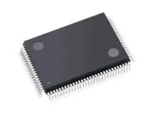
Figure 8.1. 100-Pin Package Diagram ................................................................................................................................. 50
Figure 8.2. Marking Diagram .............................................................................................................................................. 51
Figure 8.3. Alternate Topside Marking ............................................................................................................................... 51
© 2010-2017 Lattice Semiconductor Corp. All Lattice trademarks, registered trademarks, patents, and disclaimers are as listed at www.latticesemi.com/legal. All other brand or product names are
trademarks or registered trademarks of their respective holders. The specifications and information herein are subject to change without notice.
4
SiI-DS-1084-D
�SiI9136-3/SiI1136 HDMI Deep Color Transmitter
Data Sheet
Tables
Table 2.1. Product Selection Guide ...................................................................................................................................... 8
Table 4.1. Absolute Maximum Conditions .......................................................................................................................... 14
Table 4.2. Normal Operating Conditions ............................................................................................................................ 14
Table 4.3. DC Digital I/O Specifications............................................................................................................................... 15
Table 4.4. TMDS I/O Specifications ..................................................................................................................................... 15
Table 4.5. DC Specifications ................................................................................................................................................ 16
Table 4.6. Video Input AC Specifications ............................................................................................................................ 16
Table 4.7. TMDS AC Output Specifications ......................................................................................................................... 16
Table 4.8. S/PDIF Input Port Timings .................................................................................................................................. 17
Table 4.9. I2S Input Port Timings ......................................................................................................................................... 17
Table 4.10. DSD Input Port Timings .................................................................................................................................... 17
Table 4.11. Video AC Timing Specifications ........................................................................................................................ 18
Table 4.12. Control Signal Timing Specifications ................................................................................................................ 18
Table 6.1. RGB to YCbCr Conversion Formulas ................................................................................................................... 26
Table 6.2. YCbCr-to-RGB Conversion Formula .................................................................................................................... 26
Table 6.3. Control of the Default I2C Addresses with the CI2CA Pin ................................................................................... 27
Table 6.4. Supported MCLK Frequencies ............................................................................................................................ 28
Table 6.5. Channel Status Bits Used for Word Length ........................................................................................................ 28
Table 6.6. Supported 3D and 4K Video Formats ................................................................................................................. 31
Table 6.7. Video Input Formats .......................................................................................................................................... 33
Table 6.8. RGB/YCbCr 4:4:4 Separate Sync Data Mapping ................................................................................................. 34
Table 6.9. YC 4:2:2 Separate Sync Data Mapping ............................................................................................................... 36
Table 6.10. YC 4:2:2 Embedded Sync Data Mapping .......................................................................................................... 38
Table 6.11. YC Mux 4:2:2 Separate Sync Data Mapping ..................................................................................................... 40
Table 6.12. YC Mux 4:2:2 Embedded Sync Data Mapping .................................................................................................. 42
Table 6.13. RGB/YCbCr 4:4:4 Separate Sync Dual-Edge Data Mapping .............................................................................. 44
© 2010-2017 Lattice Semiconductor Corp. All Lattice trademarks, registered trademarks, patents, and disclaimers are as listed at www.latticesemi.com/legal. All other brand or product names are
trademarks or registered trademarks of their respective holders. The specifications and information herein are subject to change without notice.
SiI-DS-1084-D
5
�SiI9136-3/SiI1136 HDMI Deep Color Transmitter
Data Sheet
Acronyms in This Document
A list of acronyms used in this document.
Acronym
ACPI
Definition
Advanced Configuration and Power Interface
CBUS
Control Bus
CEC
Consumer Electronics Control
CPI
CEC Programming Interface
CSC
Color Space Converters
DDC
Display Data Channel
DSC
Display Stream Compression
DVI
Digital Visual Interface
EDDC
Enhanced Display Data Channel
EDID
Extended Display Identification Data
EMI
Electromagnetic interference
ESD
Electrostatic Discharge
GPIO
General Purpose Input/Output
HDCP
High-bandwidth Digital Content Protection
HDMI
High-Definition Multimedia Interface
HDTV
High-Definition Television
HPD
Hot Plug Detect
I2C
Inter-Integrated Circuit
KSV
Key Selection Vector
MCLK
Master Clock
SPDIF
Sony/Philips Digital Interface Format
TMDS
Transition Minimized Differential Signaling
TPI
Transmitter Programming Interface
VSIF
Vendor Specific InfoFrame
© 2010-2017 Lattice Semiconductor Corp. All Lattice trademarks, registered trademarks, patents, and disclaimers are as listed at www.latticesemi.com/legal. All other brand or product names are
trademarks or registered trademarks of their respective holders. The specifications and information herein are subject to change without notice.
6
SiI-DS-1084-D
�SiI9136-3/SiI1136 HDMI Deep Color Transmitter
Data Sheet
1. General Description
1.3.
The Lattice Semiconductor SiI9136-3/SiI1136
transmitter is an HDMI® Deep Color transmitter with
3D and 4K x 2K support for consumer electronics
products such as set-top boxes, Blu-ray players and
recorders, A/V Receivers, DVD players and recorders,
personal video recorders, home theater-in-a-box
systems, and home theater PCs. Figure 1.1 shows an
example of system architecture using the
SiI9136-3/SiI1136 device.
The SiI9136-3/SiI1136 transmitter, with the latest
generation 300 MHz TMDS™ core, enables home
theater devices to deliver up to 16-bit Deep Color at
1080p/30 resolutions and up to 12-bit Deep Color at
1080p/60 resolutions. On the audio side, high bitrate
audio formats such as Dolby® TrueHD and DTS-HD are
supported for an enhanced digital audio experience.
1.1.
Video Input
Supports most common standard and
nonstandard video input formats
Supports most common 3D formats
Supports video resolutions up to 8-bit 4K (30 Hz),
12-bit 1080p (60 Hz), 12-bit 720p/1080i (120 Hz),
and 16-bit 1080p (30 Hz)
DVI, HDCP (on SiI9136-3 only), and HDMI
transmitter with xvYCC extended color gamut,
Deep Color up to 16-bit color, 3D, and high bitrate
audio support
300 MHz HDMI transmitter
Supports all mandatory and some optional 3D
modes
Preprogrammed HDCP key set (on SiI9136-3 only)
simplifies the manufacturing process, lowers cost,
and provides the highest level of HDCP key
security
1.4.
Audio Input
S/PDIF input supports PCM and compressed audio
formats (Dolby Digital, DTS, AC-3)
DSD input supports Super Audio CD applications
(SACD)
I²S input supports PCM, DVD-Audio input (up to
8-channel 192 kHz)
High Bitrate audio support such as DTS HD and
Dolby True HD
Control Capability
Consumer Electronics Control (CEC) interface that
incorporates an HDMI-compliant CEC I/O and the
Lattice CEC Programming Interface (CPI) reduces
the need for system-level control by the system
microcontroller and simplifies firmware overhead
Four General Purpose I/O (GPIO) pins
Three dynamic power management modes as
required in the Advanced Configuration and Power
Interface (ACPI) Specification, according to system
needs
1.5.
1.2.
HDMI Output
Packaging
100-pin, 14 mm x 14 mm, 0.5 mm pitch TQFP
package with ePad
Figure 1.1. Typical Application for Streaming Sticks
© 2010-2017 Lattice Semiconductor Corp. All Lattice trademarks, registered trademarks, patents, and disclaimers are as listed at www.latticesemi.com/legal. All other brand or product names are
trademarks or registered trademarks of their respective holders. The specifications and information herein are subject to change without notice.
SiI-DS-1084-D
7
�SiI9136-3/SiI1136 HDMI Deep Color Transmitter
Data Sheet
2. Product Family
Table 2.1 summarizes the differences between the SiI9136-3/SiI1136 transmitter and the SiI9134 transmitter.
Table 2.1. Product Selection Guide
Transmitter
Video Input
Digital Video Input Ports
I/O Voltage
Core Voltage
SiI9134
SiI9136
SiI9136-3/SiI1136
1
1
1
3.3 V
3.3 V
3.3 V
1.8 V
1.2 V
1.2 V
Input Pixel Clock Multiply/Divide
0.5x, 2x, 4x
0.5x, 2x, 4x
0.5x, 2x, 4x
Maximum Pixel Input Clock Rate
165 MHz
165 MHz
300 MHz
Maximum TMDS Output Clock
225 MHz
225 MHz
300 MHz
BTA-T1004 Format Support
Video Format Conversion
36-bit and 30-bit Deep Color
Yes
Yes
Yes
Yes
Yes
Yes
48-bit Deep Color
No
Yes
Yes
xvYCC
No
Yes
Yes
YCbCr RGB CSC
Yes
Yes
Yes
RGB YCbCr CSC
Yes
Yes
Yes
4:2:2 4:4:4 Upsampling
Yes
Yes
Yes
4:4:4 4:2:2 Decimation
Yes
Yes
Yes
16–235 0–255 Expansion
Yes
Yes
Yes
0–255 16–235 Compression
Yes
Yes
Yes
16–235/240 Clipping
Audio Input
S/PDIF Input Ports
Yes
Yes
Yes
1
1
1
4 (8-channel)
4 (8-channel)
4 (8-channel)
High Bitrate Audio Support
Compressed DTS-HD and Dolby True-HD
Yes
Yes
Yes
One-bit Audio (DSD/SACD)
Yes
Yes1
Yes1
192 kHz on I2S
192 kHz on S/PDIF
192 kHz on I2S
192 kHz on S/PDIF
192 kHz on I2S
192 kHz on S/PDIF
I2S Input Bits
2-Channel Maximum Sample Rate
8-Channel Maximum Sample Rate
Down Sampling
Internal MCLK Generator
I2C Address Bus
Device Address Select
192 kHz
192 kHz
192 kHz
96 kHz to 48 kHz
192 kHz to 48 kHz
96 kHz to 48 kHz
192 kHz to 48 kHz
96 kHz to 48 kHz
192 kHz to 48 kHz
No
Yes2
Yes2
CI2CA Pin
CI2CA Pin
CI2CA Pin
Master DDC Bus
Other
CEC Interface
Yes
Yes
Yes
No
Yes
Yes
xvYCC Gamut Data
Yes
Yes
Yes
3D Support
Yes
Yes
Yes
Programming Interface
HDCP Reset
No
Yes
Yes
Software Register
Software Register
Software Register
100-pin TQFP
100-pin TQFP
Package
100-pin TQFP
Notes:
1. Shared with I2S Input Interface.
2. Internal MCLK generation is ON by default.
3. HDCP Reset does not apply to the SiI1136 transmitter.
© 2010-2017 Lattice Semiconductor Corp. All Lattice trademarks, registered trademarks, patents, and disclaimers are as listed at www.latticesemi.com/legal. All other brand or product names are
trademarks or registered trademarks of their respective holders. The specifications and information herein are subject to change without notice.
8
SiI-DS-1084-D
�SiI9136-3/SiI1136 HDMI Deep Color Transmitter
Data Sheet
3. Functional Description
Figure 3.1 shows the functional diagram of the SiI9136-3/SiI1136 transmitter. Pin descriptions begin on page 23. A
description of each of the blocks shown in the diagram follows the figure. The power domains are described in the Power
Domains section on page 29.
Note:
HDCP blocks do not apply to the SiI1136 transmitter.
CEC
Interface
I2C Slave
Interface
CSDA
CSCL
DDC Master
I2C Interface
Configuration
Logic and
Registers
CI2CA
CEC
DSDA
DSCL
INT
RESET#
Hot Plug Detect
Hot-Plug
Detector
Receiver Sense
and Interrupt Logic
GPIO
HPD
GPIO[3:0]
IDCK
D[35:0]
Video Data Input
and Conversion
HSYNC
EXT_SWING
VSYNC
DE
HDCP
ROM
SPDIF_IN
MCLK
SCK
TMDS
Transmitter
TX0±
TX1±
TX2±
Audio Data
Capture
WS
TXC±
HDCP
Encryption
Engine
XOR
Mask
Framer
SD[3:0]
DL[3],DR[3]
Figure 3.1. SiI9136-3/SiI1136 Functional Block Diagram
3.1.
Video Data Input and Conversion
Figure 3.2 shows the video data processing stages through the transmitter. Each of the processing blocks can be
bypassed by setting the appropriate register bits. The HSYNC and VSYNC input signals are required, except in
embedded sync modes. The DE input signal is optional, because it can be created with the DE generator using the
HSYNC and VSYNC signals.
IDCK
Input
Clock
Multiplier/
Divider
Clock
Data
Embedded
Sync Decoder
D[35:0]
Video
Data
Capture
DE
HSYNC,
VSYNC
HSYNC,
VSYNC
Combiner
DE
Data
Enable
Generator
HSYNC
VSYNC
DE
4:2:2 to 4:4:4
Upsampler
bypass 422
YCbCr to
RGB Color
Space Converter
bypass CSC
DE can be explicit input,
decoded from embedded
syncs, or generated from
Hsync and Vsync edges.
external DE
RGB
Range
Expansion
RGB to
YCbCr Color
Space Converter
RGB/YCbCr
Range
Compression
4:4:4 to 4:2:2
Downsampler
Clipping
Dither
18 to
8/10/12/16
bypass Expansion
bypass CSC
bypass Compression
bypass 444
bypass Clipping
bypass Dither
To HDCP XOR Mask
Figure 3.2. Transmitter Video Data Processing Path
© 2010-2017 Lattice Semiconductor Corp. All Lattice trademarks, registered trademarks, patents, and disclaimers are as listed at www.latticesemi.com/legal. All other brand or product names are
trademarks or registered trademarks of their respective holders. The specifications and information herein are subject to change without notice.
SiI-DS-1084-D
9
�SiI9136-3/SiI1136 HDMI Deep Color Transmitter
Data Sheet
3.1.1. Input Clock Multiplier/Divider
The input pixel clock can be multiplied by 0.5, 2, or 4. Video input formats that use a 2x clock, such as YC Mux mode,
can be transmitted across the HDMI link with a 1x clock. Similarly, 1x-to-2x, 1x-to-4x, and 2x-to-4x conversions are
possible.
3.1.2. Video Data Capture
The bus configurations support most standardized video input formats as well as other widely used non-standard
formats. Each configuration has four key attributes: data width, input mode, clock mode, and synchronization.
The video input port is a 36-bit wide bus that can be configured to any of the following data widths:
8-, 10-, or 12-bit input in double speed clock mode
12-, 15-, 18-, or 24-bit input in dual edge clock mode
16-, 20-, 24-, 30-, or 36-input in single speed clock mode
The input mode includes color format such as RGB, YCbCr, or xvYCC, and color sampling such as 4:4:4 or 4:2:2.
Clock mode refers to the input clock rate relative to the pixel clock rate. The SiI9136-3/SiI1136 device supports 1x mode
and 2x mode, or dual edge mode. 1x mode and 2x mode means that the input clock operates at one or two times the
pixel clock rate. Dual edge mode means that the input clock rate equals the pixel clock rate, but a sample is captured
on both the rising edge and the falling edge of the input clock. Thus, with the Video Input configured for 24 bits with a
dual edge clock, 48 bits of video data are received per clock cycle. The 24 MSBs of the video data are latched on the
first clock edge, and the 24 LSBs are latched on the next clock edge. The first clock edge is programmable and can be
either the rising or falling edge.
Synchronization attributes refer to how the horizontal and vertical sync signals are configured. Separate
synchronization involves placing the horizontal sync, vertical sync, and data enable signals on separate input pins.
Embedded synchronization combines these signals with one or more of the data inputs.
3.1.3. Embedded Sync Decoder
The transmitter can create DE, HSYNC, and VSYNC signals using the Start of Active Video (SAV) and End of Active Video
(EAV) codes within the ITU-R BT.656-format video stream.
3.1.4. Data Enable Generator
The transmitter includes logic to construct a Data Enable (DE) signal from the incoming HSYNC, VSYNC, and IDCK. This
signal is used to correct timing from sync extraction to conform to CEA-861D timing specifications. By programming
registers, the DE signal can define the size of the active display region. This feature is particularly useful when the
transmitter connects to MPEG decoders that do not provide a specific DE output signal.
3.1.5. Combiner
The clock, data, and sync information is combined into a complete set of signals required for TMDS encoding. From
here, the signals are manipulated by the register-selected video processing blocks.
3.1.6. 4:2:2 to 4:4:4 Upsampler
Chrominance upsampling doubles the number of chrominance samples per line, converting 4:2:2 sampled video to
4:4:4.
3.1.7. RGB Range Expansion
The SiI9136-3/SiI1136 transmitter can scale the input color range from limited-range into full-range using the range
expansion block. When enabled by itself, the range expansion block expands 16–235 (64–943 to 256–3775, 409660415 for 30/36/48-bit color depth) limited-range data into 0–255 (0–1023, 0–4095 to 0-65535 for 30/36/48-bit color
depth) full-range data for each video channel. When range expansion and the YCbCr to RGB color space converter are
both enabled, the input conversion range for the Cb and Cr channels is 16–240 (64–963, 256–3855 to 4096-61695 for
30/36/48-bit color depth).
© 2010-2017 Lattice Semiconductor Corp. All Lattice trademarks, registered trademarks, patents, and disclaimers are as listed at www.latticesemi.com/legal. All other brand or product names are
trademarks or registered trademarks of their respective holders. The specifications and information herein are subject to change without notice.
10
SiI-DS-1084-D
�SiI9136-3/SiI1136 HDMI Deep Color Transmitter
Data Sheet
3.1.8. Color Space Converter
Two Color Space Converters (CSCs) (YCbCr to RGB and RGB to YCbCr) are available to interface to the many video
formats supplied by A/V processors and to provide full DVI backward compatibility. The CSC can be adjusted to perform
standard-definition conversions (ITU.601) or high-definition conversions (ITU.709) by setting the appropriate registers.
3.1.9. RGB/YCbCr Range Compression
When enabled by itself, the range compression block compresses 0–255/0–1023/0–4095/0–65535 full-range data into
16–235/64–943/256–3775/4096–60415 limited-range data for each video channel. When enabled with the RGB to
YCbCr converter, this block compresses to 16–240/64–963/256–3855/4096–61695 for the Cb and Cr channels. The
color range scaling is linear.
3.1.10. 4:4:4 to 4:2:2 Downsampler
Downsampling reduces the number of chrominance samples per line by half, converting 4:4:4 sampled video to 4:2:2.
3.1.11. Clipping
The clipping block, when enabled, clips the values of the output video to 16–235 for RGB video or the Y channel, and to
16–240 for the Cb and Cr channels.
3.1.12. 18-to-8/10/12/16-Dither
The 18-to-8/10/12/16-dither block dithers internally processed, 18-bit data to 8, 10, 12, or 16 bits for output on the
HDMI link. It can be bypassed to output 10/12-bit modes when supplied by the A/V processor or converted in the
decimator and CSC.
3.2.
Audio Data Capture
The audio capture block supports I2S, Direct Stream Digital, and S/PDIF audio input formats. The appropriate registers
must be configured to describe the audio format provided to the SiI9136-3/SiI1136 transmitter. This information is
passed over the HDMI link in the CEA-861D Audio Info (AI) packets.
3.3.
Framer
The framer block handles the packetizing and framing of the data stream sent across the HDMI link. Audio and video
data packets are inserted into the respective HDMI Video Data and Data Island periods. This block handles the correct
insertion of all HDMI packet types.
3.4.
HDCP Encryption Engine/XOR Mask
The HDCP encryption engine contains the logic necessary to encrypt the incoming audio and video data and includes
support for HDCP authentication and repeater checks. The system microcontroller or microprocessor controls the
encryption process by using a set sequence of register reads and writes. An algorithm uses HDCP keys and a Key
Selection Vector (KSV) stored in the HDCP key ROM to calculate a number that is then applied to an XOR mask. This
process encrypts the audio and video data on a pixel-by-pixel basis during each clock cycle. The HDCP encryption
engine/XOR mask does not apply to the SiI1136 transmitter.
© 2010-2017 Lattice Semiconductor Corp. All Lattice trademarks, registered trademarks, patents, and disclaimers are as listed at www.latticesemi.com/legal. All other brand or product names are
trademarks or registered trademarks of their respective holders. The specifications and information herein are subject to change without notice.
SiI-DS-1084-D
11
�SiI9136-3/SiI1136 HDMI Deep Color Transmitter
Data Sheet
3.5.
HDCP Key ROM
The SiI9136-3/SiI1136 transmitter comes preprogrammed with a set of production HDCP keys stored in an internal
ROM. System manufacturers do not need to purchase key sets from the Digital-Content Protection LLC. Lattice
Semiconductor handles all purchasing, programming, and security for the HDCP keys. The preprogrammed HDCP keys
provide the highest level of security because there is no way to read the keys once the device is programmed.
Customers must sign the HDCP license agreement (www.digital-cp.com) or be under a specific NDA with Lattice
Semiconductor before receiving SiI9136-3/SiI1136 samples.
The SiI1136 transmitter is functionally equivalent to the SiI9136-3 except the HDCP keys are not preprogrammed and
therefore does not support HDCP encryption.
3.6.
TMDS Transmitter
The TMDS digital core performs 8-to-10-bit TMDS encoding on the data received from the HDCP XOR mask, and is then
sent over three TMDS data and a TMDS clock differential lines. A resistor connected to the EXT_SWING pin controls the
swing amplitude of the TMDS signal.
3.7.
GPIO
The SiI9136-3/SiI1136 transmitter has four General Purpose I/O pins. Each pin supports the following functions:
Input mode: The value can be read through local I2C bus access; an interrupt can be generated on either the falling
or the rising edge of the input signal.
Output mode: The value can be set through the local I2C bus access.
3.8.
Hot Plug Detector
When HIGH, the Hot Plug Detection signal indicates to the transmitter that the EDID of the connected receiver is
readable. A HIGH voltage is at least 2.0 V, and a LOW voltage is less than 0.8 V.
3.9.
CEC Interface
The Consumer Electronics Control (CEC) Interface block provides CEC-compliant signals between CEC devices and a CEC
master. A CEC controller compatible with the Lattice Semiconductor CEC API is included on-chip. The controller has a
high-level register interface accessible through the I2C interface, and can be used to send and receive CEC commands.
This controller makes CEC control easy and straightforward by removing the burden of programming the host
processor to perform these low-level transactions on the CEC bus. See the CEC Programming Interface (CPI)
Programmer Reference for details on the API (see the Lattice Semiconductor Documents section on page 52). The
Programmer’s Reference requires an NDA with Lattice Semiconductor.
3.10. DDC Master I2C Interface
The host uses the DDC master logic to read the EDID by programming the target address, offset, and number of bytes.
Upon completion, or when the DDC master FIFO becomes full, an interrupt signal is sent to the host so that the host
can read data out of the FIFO.
The TPI hardware uses the DDC master logic to carry out HDCP authentication tasks. The arbitration logic arbitrates the
access from host and the internal TPI hardware. See the Internal DDC Master section on page 30 for more information.
© 2010-2017 Lattice Semiconductor Corp. All Lattice trademarks, registered trademarks, patents, and disclaimers are as listed at www.latticesemi.com/legal. All other brand or product names are
trademarks or registered trademarks of their respective holders. The specifications and information herein are subject to change without notice.
12
SiI-DS-1084-D
�SiI9136-3/SiI1136 HDMI Deep Color Transmitter
Data Sheet
3.11. Receiver Sense and Interrupt Logic
The Interrupt logic of this block buffers interrupt events from different sources. Receiver Sense and Hot Plug Interrupts
are also available in power down mode. The logic for handling these interrupts when all clocks are disabled is also part
of this block. The INT pin provides an interrupt signal to the system microcontroller when any of the following occur:
Monitor Detect (either from the HPD input level or from the Receiver Sense feature) changes
VSYNC (useful for synchronizing a microcontroller to the vertical timing interval)
Error in the audio format
DDC FIFO status change
HDCP authentication error.
3.12. Configuration Logic and Registers
This block contains the configuration registers that control the operation of the transmitter. The registers are accessed
via the I2C interface. This block also contains logic for simplifying the configuration of the transmitter by automatically
programming different parameters.
3.13. I2C Slave Interface
The controller I2C interface on the transmitter (signals CSCL and CSDA) is a slave interface with an operating frequency
from 3 kHz to 400 kHz and with an input tolerance of up to 4.0 V when all device operating voltages are present. The
host uses this interface to configure the transmitter by reading from and writing to appropriate registers.
© 2010-2017 Lattice Semiconductor Corp. All Lattice trademarks, registered trademarks, patents, and disclaimers are as listed at www.latticesemi.com/legal. All other brand or product names are
trademarks or registered trademarks of their respective holders. The specifications and information herein are subject to change without notice.
SiI-DS-1084-D
13
�SiI9136-3/SiI1136 HDMI Deep Color Transmitter
Data Sheet
4. Electrical Specifications
4.1.
Absolute Maximum Conditions
Table 4.1. Absolute Maximum Conditions
Symbol
IOVCC33
Parameter
I/O Pin Supply Voltage
Min
–0.3
Typ
—
Max
4.0
Units
V
Note
2
CVCC12
Digital Core Supply Voltage
–0.5
—
1.5
V
2
AVCC
Analog Supply Voltage 1.2 V
–0.5
—
1.5
V
2
VI
Input Voltage
–0.3
—
IOVCC + 0.3
V
—
VO
Output Voltage
–0.3
—
IOVCC + 0.3
V
—
TJ
Junction Temperature
—
—
125
C
—
TSTG
Storage Temperature
–65
—
150
C
—
Notes:
1. Permanent device damage can occur if absolute maximum conditions are exceeded.
2. Functional operation should be restricted to the conditions described in the Normal Operating Conditions section.
4.2.
Normal Operating Conditions
Table 4.2. Normal Operating Conditions
Symbol
IOVCC33
Parameter
I/O Pin Supply Voltage
Min
3.135
Typ
3.3
Max
3.465
Units
V
Note
—
CVCC12
Digital Core Supply Voltage
1.14
1.2
1.26
V
—
AVCC
Analog Supply Voltage, 1.2 V
1.14
1.2
1.26
V
—
VCCN
Supply Voltage Noise Tolerance
—
—
100
mVP-P
*
TA
Ambient Temperature (with power applied)
0
25
70
C
—
ja
Thermal Resistance (Theta JA)
—
—
29.3
C/W
—
jc
Junction to case resistance (Theta JC)
—
—
12.8
C/W
—
*Note: The supply voltage noise is measured at test point VCCTP. See Figure 4.1. The ferrite bead provides filtering of power supply
noise. The figure is representative and applies to the IOVCC33, CVCC12, and AVCC pins.
VCCTP
Ferrite
VCC
0.1 F
10 F
0.1 F
SiI9136-3/
SiI1136
1 nF
GND
Figure 4.1. VCCTP Test Point for VCC Noise Tolerance
© 2010-2017 Lattice Semiconductor Corp. All Lattice trademarks, registered trademarks, patents, and disclaimers are as listed at www.latticesemi.com/legal. All other brand or product names are
trademarks or registered trademarks of their respective holders. The specifications and information herein are subject to change without notice.
14
SiI-DS-1084-D
�SiI9136-3/SiI1136 HDMI Deep Color Transmitter
Data Sheet
4.2.1. I/O Specifications
Under normal operating conditions unless otherwise specified.
Table 4.3. DC Digital I/O Specifications
Symbol
VIH
VIL
Parameter
HIGH-level Input Voltage*
LOW-level Input Voltage*
VTH+
VTHVTH+
LOW to HIGH Threshold
HIGH to LOW Threshold
LOW to HIGH Threshold
VTHVTH+
VTH-
HIGH to LOW Threshold
LOW to HIGH Threshold
HIGH to LOW Threshold
VOH
VOL
HIGH-level Output Voltage
LOW-level Output Voltage
High Impedance Output Leakage
Current
IOZ
Signal Type
Conditions
LVTTL
—
Schmitt
RESET#, CSCL, CSDA
Schmitt
DSCL, DSDA
Schmitt
CEC_A
LVTTL
IOH
HIGH level Output Current
IOL
LOW level Output Current
*Note: All unused input signals should be tied LOW.
Min
2.0
–0.3
Typ
—
—
Max
5.5
0.8
Units
V
V
1.9
—
3.0
—
—
—
—
0.7
—
V
V
V
—
2.0
—
—
—
—
1.5
—
0.8
V
V
V
—
2.4
—
—
—
—
0.4
V
V
—
@ VO = 3.3 V or 0 V
–10
—
10
A
—
—
@ VOH {Min}
@ VOL {Max}
—
—
—
—
8
8
mA
mA
Table 4.4. TMDS I/O Specifications
Signal
Type
Conditions
Min
Typ
Max
Units
VOD
Differential outputs:
single-ended swing
amplitude*
TMDS
RLOAD = 50 Ω
REXT_SWING as defined in
the Pin Descriptions
section
400
500
600
mV
VODD
Differential outputs:
differential swing
amplitude
TMDS
—
800
1000
1200
mV
VDOH
Differential HIGH level
output voltage
TMDS
≤ 165 MHz TMDS clock
> 165 MHz TMDS clock
AVCC – 10 mV
AVCC – 200 mV
—
—
AVCC + 10 mV
AVCC + 10 mV
V
V
VDOL
Differential LOW level
output voltage
TMDS
≤ 165 MHz TMDS clock
> 165 MHz TMDS clock
AVCC – 600 mV
AVCC – 700 mV
—
—
AVCC – 400 mV
AVCC – 400 mV
V
V
IDOS
Differential output
short circuit current
TMDS
VOUT = 0 V
—
—
5
μA
Symbol
Parameter
*Note: Single-ended swing amplitude limits are defined by the HDMI Specification.
© 2010-2017 Lattice Semiconductor Corp. All Lattice trademarks, registered trademarks, patents, and disclaimers are as listed at www.latticesemi.com/legal. All other brand or product names are
trademarks or registered trademarks of their respective holders. The specifications and information herein are subject to change without notice.
SiI-DS-1084-D
15
�SiI9136-3/SiI1136 HDMI Deep Color Transmitter
Data Sheet
4.2.2. DC Power Supply Specifications
Table 4.5 shows the power consumption in the three power modes. Measurement uses Dot Moiré pattern with
8-chanel I2S audio and HDCP enabled.
Table 4.5. DC Specifications
Symbol
Parameter
Mode
IPON
Power On Current
D0
IPSTBY
IPOFF
Power Standby Current
D2
D3
Power Off current
74.25 MHz
IOVCC33
Typ
Max
1.8
1.7
AVCC
Typ
Max
10.9
12.2
CVCC12
Typ
Max
36.3
40.0
148.5 MHz
225 MHz
297 MHz
3.6
4.7
3.82
18.2
25.4
33.1
68.4
83.9
94.9
Frequency1
—
—
3.1
3.8
3.22
4.70
4.70
20.3
28.3
37.3
0.50
0.50
Units
mA
75.6
92.9
105.2
9.10
5.10
mA
mA
mA
mA
mA
Notes:
1. TMDS clock frequency does not matter in D3 and D2 modes.
2. Current measurement for IOVCC33 is lower at 297 MHz since only 24-bits per pixel is used. At 225 MHz used for deep color,
each pixel is 36-bits wide.
4.3.
AC Specifications
4.3.1. Video/HDMI Timing Specifications
Under normal operating conditions unless otherwise specified.
Table 4.6. Video Input AC Specifications
Symbol
TDDF
TDDR
Parameter
VSYNC and HSYNC Delay from DE falling
edge
VSYNC and HSYNC Delay to DE rising edge
Conditions
Min
Typ
Max
Units
Figure
—
1
—
—
TCIP
Figure 4.6
—
1
—
—
TCIP
Figure 4.6
THDE
DE HIGH Time
—
—
—
8191
TCIP
Figure 4.7
TLDE
DE LOW Time
—
138*
—
—
TCIP
Figure 4.7
*Note: TLDE minimum is defined for HDMI mode carrying 480p video with 192 kHz audio, which requires at least 138 pixel clock
cycles of blanking to carry the audio packets. If only HDCP is running, the minimum DE LOW time is 58 clock cycles, according to the
HDCP Specification. If neither HDCP nor audio are running, the minimum DE LOW time is 12 clock cycles for TMDS. The minimum
vertical blanking time is three horizontal line times.
Table 4.7. TMDS AC Output Specifications
Symbol
Parameter
SLHT
Differential Swing LOW-to-HIGH
Transition Time
SHLT
Differential Swing HIGH-to-LOW
Transition Time
Conditions
REXT_SWING = 3.83 kΩ
Internal Source
Termination On
REXT_SWING = 3.83 kΩ
Internal Source
Termination On
Min
Typ
Max
Units
Figure
95.5
—
181.81
ps
Figure 4.10
86.5
—
172.3
ps
Figure 4.10
Notes:
1. These limits are defined by the HDMI Specification.
2. Refer to the Source Termination section on page 31 for information about internal source termination.
© 2010-2017 Lattice Semiconductor Corp. All Lattice trademarks, registered trademarks, patents, and disclaimers are as listed at www.latticesemi.com/legal. All other brand or product names are
trademarks or registered trademarks of their respective holders. The specifications and information herein are subject to change without notice.
16
SiI-DS-1084-D
�SiI9136-3/SiI1136 HDMI Deep Color Transmitter
Data Sheet
4.3.2. Audio AC Timing Specifications
Table 4.8. S/PDIF Input Port Timings
Symbol
FS_SPDIF
TSPCYC
Parameter
Sample Rate
S/PDIF Cycle Time
Conditions
2 Channel
CL = 10 pF
Min
32
—
Typ
—
—
Max
192
1.0
Units
kHz
UI
Figure
—
Figure 4.12
Notes
—
1
TSPDUTY
TMCLKCYC
S/PDIF Duty Cycle
MCLK Cycle Time
CL = 10 pF
CL = 10 pF
90%
13.3
—
—
110%
—
UI
ns
Figure 4.12
Figure 4.13
1
3
FMCLK
TMCLKDUTY
MCLK Frequency
MCLK Duty Cycle
CL = 10 pF
CL = 10 pF
—
40%
—
—
75
60%
MHz
TMCLKCYC
—
Figure 4.13
3
3
TAUDDLY
Audio Pipeline Delay
—
—
30
70
s
—
4
Conditions
—
CL = 10 pF
CL = 10 pF
Min
32
—
90%
Typ
—
—
—
Max
192
1.0
110%
Units
kHz
UI
UI
Figure
—
Figure 4.11
Figure 4.11
Notes
—
1
—
CL = 10 pF
CL = 10 pF
15
0
—
—
—
—
ns
ns
Figure 4.11
Figure 4.11
2
2
Note: Refer to the notes for Table 4.10.
Table 4.9. I2S Input Port Timings
Symbol
FS_I2S
TSCKCYC
TSCKDUTY
Parameter
Sample Rate
I2S Cycle Time
I2S Duty Cycle
TI2SSU
I2S Setup Time
TI2SHD
I2S Hold Time
Note: Refer to the notes for Table 4.10.
Table 4.10. DSD Input Port Timings
Symbol
FS_DSD
Parameter
Sample Rate
Conditions
—
Min
—
Typ
44.1
Max
88.2
Units
kHz
Figure
—
Notes
—
TDCKCYC
TDCKDUTY
TDSDSU
DSD Cycle Time
DSD Duty Cycle
DSD Setup Time
CL = 10 pF
CL = 10 pF
CL = 10 pF
—
90%
20
—
—
—
2.0
110%
—
UI
UI
ns
Figure 4.14
Figure 4.14
Figure 4.14
1
1
—
TDSDHD
DSD Hold Time
CL = 10 pF
20
—
—
ns
Figure 4.14
—
Notes:
1. Proportional to unit time (UI) according to sample rate. Refer to the I2S, S/PDIF, or DSD Specifications.
2. Setup and hold minimum times are based on 13.388 MHz sampling, which is adapted from Figure 3 of the Philips I2S
Specification.
3. If a separate master clock input (MCLK) is used for time-stamping purposes, it has to be coherent with the audio input.
Coherent means that the MCLK and audio input have been created from the same clock source. This requirement usually uses
the original MCLK to strobe the audio out from the sourcing chip.
4. Audio pipeline delay is measured from the transmitter input pins to the TMDS output.
© 2010-2017 Lattice Semiconductor Corp. All Lattice trademarks, registered trademarks, patents, and disclaimers are as listed at www.latticesemi.com/legal. All other brand or product names are
trademarks or registered trademarks of their respective holders. The specifications and information herein are subject to change without notice.
SiI-DS-1084-D
17
�SiI9136-3/SiI1136 HDMI Deep Color Transmitter
Data Sheet
4.3.3. Video AC Timing Specifications
Under normal operating conditions unless otherwise specified.
Table 4.11. Video AC Timing Specifications
Symbol
TCIP
FCIP
Parameter
IDCK period, one pixel per clock
IDCK frequency, one pixel per clock
Conditions
—
—
Min
3.3
25
Typ
—
—
Max
40
300
Units
ns
MHz
Figure
Figure 4.2
—
Notes
1
1
TCIP12
FCIP12
IDCK period, dual-edge clock
IDCK frequency, dual-edge clock
—
—
12.3
25
—
—
40
82.5
ns
MHz
Figure 4.2
—
2
2
TDUTY
IDCK duty cycle
Worst case IDCK clock jitter, DJ
Worst case IDCK clock jitter, RJ
—
—
—
45%
—
—
—
—
—
55%
0.20
0.25
TCIP
TBIT
TBIT
Figure 4.2
—
—
—
TSIDF
THIDF
Setup time to IDCK falling edge
Hold time to IDCK falling edge
EDGE = 0
1.36
0.45
—
—
—
—
ns
ns
Figure 4.4
5
TSIDR
THIDR
TSIDD
Setup time to IDCK rising edge
Hold time to IDCK rising edge
Setup time to IDCK rising or falling edge
1.57
1.16
1.57
—
—
—
—
—
—
ns
ns
ns
Figure 4.3
5
TIJIT
EDGE = 1
3, 4
Dual-edge
Figure 4.5
6
clocking
THIDD
Hold time to IDCK rising or falling edge
1.16
—
—
ns
Notes:
1. TCIP and FCIP apply in single-edge clocking modes. TCIP is the inverse of FCIP and is not a controlling specification.
2. TCIP12 and FCIP12 apply in dual-edge mode. TCIP12 is the inverse of FCIP12 and is not a controlling specification.
3. TBIT is the TMDS bit time.
4. Total jitter (TJ) is calculated from DJ (deterministic jitter), RJ (random jitter, rms) and required BER (Bit Error Rate). For BER of
1E-9, TJ = DJ + 12 • RJ = 3.2 TBIT.
5. Setup and hold time specifications apply to Data, DE, VSYNC, and HSYNC input pins, relative to IDCK input clock.
6. Setup and hold limits are not affected by the setting of the EDGE bit for 12/15/18/24-bit dual-edge clocking mode.
4.3.4. Control Signal Timing Specifications
Under normal operating conditions unless otherwise specified.
Table 4.12. Control Signal Timing Specifications
Symbol
Parameter
TRESET
TI2CDVD
THDDAT
TINT
Conditions
Min
Typ
Max
Units
RESET# signal LOW time required for reset
—
50
—
—
µs
SDA Data Valid Delay from SCL falling edge
on READ command
CL = 400pF
—
—
700
0–400 kHz
2.0
—
RESET# = HIGH
—
—
I2C data hold time
Response time for INT output pin from
change in input condition (HPD, Receiver
Sense, VSYNC change, etc.).
Figure
Figure 4.8
Figure 4.9
Note
ns
Figure 4.15
2, 6
—
ns
—
3, 6
100
µs
—
—
1, 5
FSCL
Frequency on master DDC SCL signal
—
40
70
100
kHz
—
4
FCSCL
Frequency on master CSCL signal
—
40
—
400
kHz
—
—
Notes:
1. Reset on RESET# signal can be LOW as the supply becomes stable (shown in Figure 4.8), or pulled LOW for at least TRESET (shown
in Figure 4.9).
2. All standard-mode (100 kHz) I2C timing requirements are guaranteed by design. These timings apply to the slave I2C port (pins
CSDA and CSCL) and to the master I2C port (pins DSDA and DSCL).
3. This minimum hold time is required by CSCL and CSDA signals as an I2C slave. The device does not include the 300 ns internal
delay required by the I2C Specification (Version 2.1, Table 5, note 2).
4. The master DDC block provides an SCL signal for the E-DDC bus. The HDMI Specification limits this to I2C Standard Mode or 100
kHz. Use of the Master DDC block does not require an active IDCK.
5. Not a Schmitt trigger.
6. Operation of I2C pins above 100 kHz is defined by LVTTL levels VIH, VIL, VOH, and VOL (see Table 4.3 on page 15). For these levels,
I2C speeds up to 400 kHz are supported.
© 2010-2017 Lattice Semiconductor Corp. All Lattice trademarks, registered trademarks, patents, and disclaimers are as listed at www.latticesemi.com/legal. All other brand or product names are
trademarks or registered trademarks of their respective holders. The specifications and information herein are subject to change without notice.
18
SiI-DS-1084-D
�SiI9136-3/SiI1136 HDMI Deep Color Transmitter
Data Sheet
4.3.5. CEC Timing Specifications
See the HDMI 1.4 Specification – Supplement 1 Consumer Electronics Control (CEC).
4.4.
Timing Diagrams
4.4.1. Input Timing Diagrams
TCIP/TCIP12
50%
50%
50%
TDUTY
Figure 4.2. IDCK Clock Duty Cycle
TCIP
IDCK
50 %
50 %
TSIDR
D[23:0], DE,
HSYNC,VSYNC
THIDR
no change allowed
50 %
50 %
Signals may change only in the unshaded portion of the waveform, to meet both the
minimum setup and minimum hold time specifications.
Figure 4.3. Control and Data Single-Edge Setup and Hold Times—EDGE = 1
IDCK
50 %
50 %
TSIDF
D[23:0], DE,
HSYNC,VSYNC
THIDF
no change allowed
50 %
50 %
Signals may change only in the unshaded portion of the waveform, to meet both the
minimum setup and minimum hold time specifications.
Figure 4.4. Control and Data Single-Edge Setup and Hold Times—EDGE = 0
TCIP12
IDCK
50 %
TSIDD
D[11:0], DE,
HSYNC,VSYNC
50 %
50 %
THIDD
no change
allowed
TSIDD
50 %
THIDD
no change
allowed
50 %
Signals may change only in the unshaded portion of the waveform, to meet both the
minimum setup and minimum hold time specifications.
Figure 4.5. Control and Data Dual-Edge Setup and Hold Times
© 2010-2017 Lattice Semiconductor Corp. All Lattice trademarks, registered trademarks, patents, and disclaimers are as listed at www.latticesemi.com/legal. All other brand or product names are
trademarks or registered trademarks of their respective holders. The specifications and information herein are subject to change without notice.
SiI-DS-1084-D
19
�SiI9136-3/SiI1136 HDMI Deep Color Transmitter
Data Sheet
DE
50%
50%
TDDR
TDDF
VSYNC, HSYNC
50%
50%
Figure 4.6. VSYNC and HSYNC Delay Times Based on DE
THDE
DE
2.0 V
2.0 V
0.8 V
0.8 V
TLDE
Figure 4.7. DE HIGH and LOW Times
4.4.2. Reset Timing Diagrams
VCC must be stable between its limits listed in the Normal Operating Conditions section on page 14 for TRESET before RESET# goes
HIGH, as shown in Figure 4.8. Before accessing registers, RESET# must be pulled LOW for TRESET. This can be done by holding RESET#
LOW until TRESET after stable power, as described above, or by pulling RESET# LOW from a HIGH state for at least T RESET, as shown in
Figure 4.9.
VCCmax
VCCmin
VCC
RESET#
TRESET
Figure 4.8. Conditions for Use of RESET#
RESET#
TRESET
Figure 4.9. RESET# Minimum Timings
4.4.3. TMDS Timing Diagram
SLHT
SHLT
80% VOD
20% VOD
Figure 4.10. Differential Transition Times
© 2010-2017 Lattice Semiconductor Corp. All Lattice trademarks, registered trademarks, patents, and disclaimers are as listed at www.latticesemi.com/legal. All other brand or product names are
trademarks or registered trademarks of their respective holders. The specifications and information herein are subject to change without notice.
20
SiI-DS-1084-D
�SiI9136-3/SiI1136 HDMI Deep Color Transmitter
Data Sheet
4.4.4. Audio Timing Diagrams
TSCKCYC
TSCKDUTY
SCK
50 %
50 %
TI2SSU
SD[0:3], WS
TI2SHD
no change allowed
50 %
50 %
Figure 4.11. I2S Input Timings
TSPCYC
T SPDUTY
50%
SPDIF
Figure 4.12. S/PDIF Input Timings
TMCLKCYC
MCLK
50%
50%
TMCLKDUTY
Figure 4.13. MCLK Timings
TDCKCYC
TDCKDUTY
DCLK
50 %
TDSDSU
DL[3:0], DR[3:0]
50 %
TDSDHD
no change allowed
50 %
50 %
Figure 4.14. DSD Input Timings
4.4.5. I2C Timing Diagrams
CSDA, DSDA
TI2CDVD
CSCL, DSCL
Figure 4.15. I2C Data Valid Delay (Driving Read Cycle Data)
© 2010-2017 Lattice Semiconductor Corp. All Lattice trademarks, registered trademarks, patents, and disclaimers are as listed at www.latticesemi.com/legal. All other brand or product names are
trademarks or registered trademarks of their respective holders. The specifications and information herein are subject to change without notice.
SiI-DS-1084-D
21
�SiI9136-3/SiI1136 HDMI Deep Color Transmitter
Data Sheet
5. Pin Diagram and Descriptions
5.1.
Pin Diagram
63
62
61
60
59
58
57
56
55
54
NC
64
GND
NC
65
EXT_SWING
NC
66
TXC-
NC
67
AVCC
NC
68
TXC+
NC
69
TX0+
NC
70
TX0-
NC
71
TX1-
NC
72
AVCC
NC
73
TX1+
NC
74
TX2+
NC
75
TX2-
NC
Figure 5.1 shows the pin diagram for the SiI9136-3/SiI1136 transmitter. A description of the pin functions begins on the
next page.
53
52
51
HPD
76
50
GPIO1
77
49
GPIO3
D35
78
48
GND
D34
79
47
RESET#
D33
80
46
INT
D32
81
45
CSCL
D31
82
44
CSDA
D30
83
43
CI2CA
D29
84
42
DSCL
D28
85
41
DSDA
D27
86
40
CEC_A
D26
87
39
GPIO2
CVCC12
88
38
CVCC12
D25
89
37
IOVCC33
D24
90
36
MCLK
IOVCC33
91
35
SCK
D23
92
34
WS_DR0
D22
93
33
SD0_DL0
D21
94
32
SD1_DR1
D20
95
31
SD2_DL1
D19
96
30
SD3_DR2
D18
97
29
SPDIF_IN_DL2
D17
98
28
DR3
D16
99
27
DL3
GND
100
26
GPIO0
SiI9136-3
SiI9136-3/SiI1136
(TopView)
View)
(Top
D9
17
18
19
20
21
22
23
24
25
DE
D10
16
HSYNC
D11
15
IDCK
D12
14
VSYNC
CVCC12
13
D0
D13
12
CVCC12
D14
11
D1
D15
10
D2
9
D3
8
D4
7
CVCC12
6
D5
5
D6
4
IOVCC33
3
D7
2
D8
1
IOVCC33
ePad (GND)
NC
Figure 5.1. Pin Diagram
© 2010-2017 Lattice Semiconductor Corp. All Lattice trademarks, registered trademarks, patents, and disclaimers are as listed at www.latticesemi.com/legal. All other brand or product names are
trademarks or registered trademarks of their respective holders. The specifications and information herein are subject to change without notice.
22
SiI-DS-1084-D
�SiI9136-3/SiI1136 HDMI Deep Color Transmitter
Data Sheet
5.2.
Pin Descriptions
5.2.1. Video Data Input
Name
D0
Pin
20
D1
19
D2
18
D3
17
D4
15
D5
14
D6
13
D7
11
D8
10
D9
9
D10
8
D11
7
D12
6
D13
4
D14
3
D15
2
D16
99
D17
98
D18
97
D19
96
D20
95
D21
94
D22
93
D23
92
D24
90
D25
89
D26
87
D27
86
D28
85
D29
84
D30
83
D31
82
D32
81
D33
80
D34
79
D35
78
IDCK
Type
Dir
Description
LVTTL
5 V tolerant
Input
Video Data Inputs.
The video data inputs can be configured to support a wide variety of input
formats, including multiple RGB and YCbCr bus formats, using the VID_CONFIG
registers.
See the Common Video Input Formats section on page 33 for details.
22
LVTTL
5 V tolerant
Input
Input Data Clock.
Input configurable using the VID_CONFIG registers.
DE
25
LVTTL
5 V tolerant
Input
Data Enable.
This signal is HIGH when the transmitter input pixel data is valid and LOW
otherwise. DE is optional for some input formats, such as ITU-R BT.656.
HSYNC
24
LVTTL
5 V tolerant
Input
Horizontal Sync input control signal.
HSYNC is optional for some input formats, such as ITU-R BT.656.
VSYNC
23
LVTTL
5 V tolerant
Input
Vertical Sync input control signal.
VSYNC is optional for some input formats, such as ITU-R BT.656.
© 2010-2017 Lattice Semiconductor Corp. All Lattice trademarks, registered trademarks, patents, and disclaimers are as listed at www.latticesemi.com/legal. All other brand or product names are
trademarks or registered trademarks of their respective holders. The specifications and information herein are subject to change without notice.
SiI-DS-1084-D
23
�SiI9136-3/SiI1136 HDMI Deep Color Transmitter
Data Sheet
5.2.2. TMDS Output
Name
TX0+
Pin
58
TX0-
57
TX1+
60
TX1-
59
TX2+
63
TX2-
62
TXC+
55
TXC-
54
EXT_SWING
52
Type
Dir
Description
TMDS
Output
HDMI Transmitter Output Port Data.
TMDS low voltage differential signal output data pairs.
TMDS
Output
HDMI Transmitter Output Port Clock.
TMDS low voltage differential signal output clock pair.
Analog
Input
Output
External Swing Voltage Control.
Recommended values (actual value depends on board design):
5.6 k resistor to ground without using internal termination.
4.02 k resistor to ground using internal termination.
5.2.3. Audio Input
Description
I2S Mode; S/PDIF Mode
DSD Mode
Input
Audio Input Master Clock.
—
LVTTL
5 V tolerant
Input
I2S Serial Clock.
DSD Clock.
34
LVTTL
5 V tolerant
Input
I2S Word Select.
DSD Data Right Bit 0.
SD0_DL0
33
LVTTL
5 V tolerant
Input
I2S Data 0.
DSD Data Left Bit 0.
SD1_DR1
32
LVTTL
5 V tolerant
Input
I2S Data 1.
DSD Data Right Bit 1.
SD2_DL1
31
LVTTL
5 V tolerant
Input
I2S Data 2.
DSD Data Left Bit 1.
SD3_DR2
30
LVTTL
5 V tolerant
Input
I2S Data 3.
DSD Data Right Bit 2.
SPDIF_IN_DL2
29
LVTTL
5 V tolerant
Input
S/PDIF Input.
DSD Data Left Bit 2.
DR3
28
LVTTL
5 V tolerant
Input
—
DSD Data Right Bit 3.
DL3
27
LVTTL
5 V tolerant
Input
—
DSD Data Left Bit 3.
Name
Pin
Type
Dir
MCLK
36
LVTTL
5 V tolerant
SCK
35
WS_DR0
© 2010-2017 Lattice Semiconductor Corp. All Lattice trademarks, registered trademarks, patents, and disclaimers are as listed at www.latticesemi.com/legal. All other brand or product names are
trademarks or registered trademarks of their respective holders. The specifications and information herein are subject to change without notice.
24
SiI-DS-1084-D
�SiI9136-3/SiI1136 HDMI Deep Color Transmitter
Data Sheet
5.2.4. DDC, CEC, Configuration, and Control
Name
INT
Pin
46
Type
LVTTL
Dir
Output
Description
Interrupt Output.
RESET#
47
Schmitt
Input
Reset signal.
Active LOW asynchronous reset input for entire chip.
HPD
76
LVTTL
Input
Hot Plug Detect.
General Purpose I/O Data 0.
GPIO0
26
LVTTL
Input
Output
GPIO1
77
LVTTL
Input
Output
General Purpose I/O Data 1.
GPIO2
39
LVTTL
Input
Output
General Purpose I/O Data 2.
GPIO3
49
LVTTL
Input
Output
General Purpose I/O Data 3.
DSCL
42
Schmitt
Open drain
5 V tolerant
Input
Output
DDC I2C Clock.
HDCP KSV, An, and Ri values are exchanged over this I2C port during
authentication. True open drain, so does not pull to ground if power not
applied.
DSDA
41
Schmitt
Open drain
5 V tolerant
Input
Output
DDC I2C Data.
HDCP KSV, An, and Ri values are exchanged over this I2C port during
authentication. True open drain, it does not pull to ground if power not applied.
CI2CA
43
LVTTL
5 V tolerant
Input
Selects base address group for CSCL/CSDA interface. See Table 6.3 on page 27.
CSCL
45
Schmitt
5 V tolerant
Input
Local Configuration/Status I2C Clock.
Chip configuration/status registers are accessed through this I2C port.
CSDA
44
Schmitt
Open drain
5 V tolerant
Input
Output
Local Configuration/Status I2C Data.
Chip configuration/status registers are accessed through this I2C port.
CEC_A
40
CEC Compliant Input
5 V tolerant
Output
HDMI compliant CEC I/O.
As an input, this pin acts as a LVTTL Schmitt-triggered input and is 5 V tolerant.
As an output, the pin acts as an NMOS driver with resistive pull-up. This pin has
an internal pull-up resistor.
5.2.5. Power and Ground
Name
CVCC12
Pin
5, 16, 21, 38, 88
Type
Power
Description
Digital Core VCC.
Supply
1.2 V
IOVCC33
1, 12, 37, 91
Power
I/O VCC.
3.3 V
AVCC
56, 61
Power
Analog VCC.
1.2 V
GND
48, 53, 100
Ground
These pins must be connected to ground.
Ground
Description
These pins should be left unconnected.
Supply
None
5.2.6. Not Connected and Reserved
Name
NC
Pin
50, 51, 64–75
Type
Not connected
© 2010-2017 Lattice Semiconductor Corp. All Lattice trademarks, registered trademarks, patents, and disclaimers are as listed at www.latticesemi.com/legal. All other brand or product names are
trademarks or registered trademarks of their respective holders. The specifications and information herein are subject to change without notice.
SiI-DS-1084-D
25
�SiI9136-3/SiI1136 HDMI Deep Color Transmitter
Data Sheet
6. Feature Information
6.1.
RGB to YCbCr Color Space Converter
The RGBYCbCr color space converter can convert from video data RGB to standard definition or to high definition
YCbCr formats. Table 6.1 shows the conversion formulas that are used. The HDMI AVI packet defines the color space of
the incoming video.
Table 6.1. RGB to YCbCr Conversion Formulas
Video Format
Conversion
640 x 480
480i
ITU-R BT.601
ITU-R BT.601
576i
480p
576p
ITU-R BT.601
ITU-R BT.601
ITU-R BT.601
240p
288p
ITU-R BT.601
ITU-R BT.601
720p
1080i
1080p
ITU-R BT.709
ITU-R BT.709
ITU-R BT.709
6.2.
Formulas
CE Mode 16-235 RGB
Y = 0.299R′ + 0.587G′ + 0.114B′
Cb = –0.172R′ – 0.339G′ + 0.511B′ + 128
Cr = 0.511R′ – 0.428G′ – 0.083B′ + 128
Y = 0.213R′ + 0.715G′ + 0.072B′
Cb = –0.117R′ – 0.394G′ + 0.511B′ + 128
Cr = 0.511R′ – 0.464G′ – 0.047B′ + 128
YCbCr to RGB Color Space Converter
The YCbCrRGB color space converter allows MPEG decoders to interface with RGB-only inputs. The CSC can convert
from YCbCr in standard-definition (ITU.601) or high-definition (ITU.709) to RGB. See the detailed formulas in Table 6.2.
Note the difference between RGB range for CE modes and PC modes.
Table 6.2. YCbCr-to-RGB Conversion Formula
Format change
Conversion
YCbCr 16-235 Input2, 3, 4
to
RGB 16-235 Output2, 3, 4
YCbCr 16-235 Input2, 3, 4
to
RGB 0-255 Output2, 3, 4
6011
7091
601
709
YCbCr Input Color Range2, 3
R′ = Y + 1.371(Cr – 128)
G′ = Y – 0.698(Cr – 128) – 0.336(Cb – 128)
B′ = Y + 1.732(Cb – 128)
R′ = Y + 1.540(Cr – 128)
G′ = Y – 0.459(Cr – 128) – 0.183(Cb – 128)
B′ = Y + 1.816(Cb – 128)
R′ = 1.164((Y-16) + 1.371(Cr – 128))
G′ = 1.164((Y-16) – 0.698(Cr – 128) – 0.336(Cb – 128))
B′ = 1.164((Y-16) + 1.732(Cb – 128))
R′ = 1.164((Y-16) + 1.540(Cr – 128))
G′ = 1.164((Y-16) – 0.459(Cr – 128) – 0.183(Cb – 128))
B′ = 1.164((Y-16) + 1.816(Cb – 128))
Notes:
1.
2.
3.
4.
No clipping can be done.
For 10-bit deep color, multiply all occurrences of the values 16, 128, 235, and 255 by 4.
For 12-bit deep color, multiply all occurrences of the values 16, 128, 235, and 255 by 16.
For 16-bit deep color, multiply all occurrences of the values 16, 128, 235, and 255 256.
© 2010-2017 Lattice Semiconductor Corp. All Lattice trademarks, registered trademarks, patents, and disclaimers are as listed at www.latticesemi.com/legal. All other brand or product names are
trademarks or registered trademarks of their respective holders. The specifications and information herein are subject to change without notice.
26
SiI-DS-1084-D
�SiI9136-3/SiI1136 HDMI Deep Color Transmitter
Data Sheet
6.3.
I2C Register Information
I2C registers monitor and control all functions of the transmitter. The four local I 2C slave addresses can be altered by
setting the CI2CA signal LOW or HIGH as shown in Table 6.3. An external pull-up or pull-down resistor, depending on
the desired set of I2C addresses, is used to set the level on the CI2CA pin. Refer to the Programmer Reference (see the
Lattice Semiconductor Documents section on page 52) for complete information. The Programmer’s Reference requires
an NDA with Lattice Semiconductor.
Table 6.3. Control of the Default I2C Addresses with the CI2CA Pin
Block
Configuration Registers
TPI
CI2CA = 0
0x7A
0x72
CI2CA = 1
0x7E
0x76
CPI
0xC0
0xC4
6.4.
I2S Audio Input
The I2S input has four I2S data signals to support up to eight channels of linear pulse code modulation (LPCM) audio.
The I2S interface also supports high bit rate audio formats such as Dolby ® TrueHD and DTS HD Master Audio. Twochannel PCM audio can be downsampled by a factor of 2 or 4 to support 32, 44.1, or 48 kHz basic sample rates as
required by the HDMI standard.
6.5.
Direct Stream Digital Input
Nine pins are used for the Direct Stream Digital interface that provides 8-channel one-bit audio data (DSD). This
interface is for SACD applications. Seven of the nine pins of this interface (four data left, four data right, and one clock)
share the I2S and S/PDIF pins.
The one-bit audio inputs are sampled on the positive edge of the DSD clock, assembled into 56-bit packets, and
mapped to the appropriate FIFO. The Audio InfoFrame, instead of the Channel Status bits, carries the sampling
information for one-bit audio. The one-bit audio interface supports an input clock frequency of 2.882 MHz (64 • 44.1
kHz).
6.6.
S/PDIF Input
The Sony/Philips Digital Interface Format (S/PDIF) interface is usually associated with compressed audio formats such
as Dolby® Digital (AC-3), DTS, and the more advanced variants of these formats.
6.7.
I2S and S/PDIF Supported MCLK Frequencies
The transmitter includes an integrated MCLK generator for operation without an external clock PLL, although an
external MCLK can be used. The I2S and S/PDIF interfaces support sampling frequencies of 32, 44.1, 48, 64, 88.2, 96,
128, 176.4, and 192 kHz. The 64 and 128 kHz sampling rates, however, are not part of the HDMI standard; and must be
downsampled to 32 kHz before transmitting across the HDMI link. Table 6.4 lists the supported MCLK frequencies.
© 2010-2017 Lattice Semiconductor Corp. All Lattice trademarks, registered trademarks, patents, and disclaimers are as listed at www.latticesemi.com/legal. All other brand or product names are
trademarks or registered trademarks of their respective holders. The specifications and information herein are subject to change without notice.
SiI-DS-1084-D
27
�SiI9136-3/SiI1136 HDMI Deep Color Transmitter
Data Sheet
Table 6.4. Supported MCLK Frequencies
128
32 kHz
4.096 MHz
44.1 kHz
5.645 MHz
Audio Sample Rate, Fs
I2S and S/PDIF Supported Rates
48 kHz
88.2 kHz
96 kHz
6.144 MHz
11.290 MHz
12.288 MHz
192
256
6.144 MHz
8.192 MHz
8.467 MHz
11.290 MHz
9.216 MHz
12.288 MHz
16.934 MHz
22.579 MHz
18.432 MHz
24.576 MHz
33.868 MHz
45.158 MHz
36.864 MHz
49.152 MHz
384
512
768
12.288 MHz
16.384 MHz
24.576 MHz
16.934 MHz
22.579 MHz
33.869 MHz
18.432 MHz
24.576 MHz
36.864 MHz
33.864 MHz
45.158 MHz
67.738 MHz
36.864 MHz
49.152 MHz
73.728 MHz
67.737 MHz
73.728 MHz
1024
1152
32.768 MHz
36.864 MHz
45.158 MHz
50.803 MHz
49.152 MHz
55.296 MHz
Multiple of Fs
6.8.
176.4 kHz
22.579 MHz
192 kHz
24.576 MHz
Audio Downsampler Limitations
The SiI9136-3/SiI1136 transmitter has an audio downsampler function that downsamples the incoming two-channel
audio data and sends the result over the HDMI link. The audio data can be downsampled by one-half or one-fourth
with register control. Supported conversions are: from 192 kHz to 48 kHz, 176.4 kHz to 44.1 kHz, 96 kHz to 48 kHz, and
88.2 kHz to 44.1 kHz. Some limitations in the audio sample word length when using this feature may need special
consideration in a real application.
When enabling the audio downsampler, the Channel Status registers for the audio sample word lengths sent over the
HDMI link always indicate the maximum possible length. For example, if the input S/PDIF stream was in 20-bit mode
with 16 bits valid, after enabling the downsampler the Channel Status indicates 20-bit mode with 20 bits valid.
Audio sample word length is carried in bits 33 through 35 of the Channel Status register over the HDMI link, as shown
in Table 6.5. These bits are always set to 0b101 when enabling the downsampler feature. Audio data is not affected
because 0s are placed into the LSBs of the data, and the wider word length is sent across the HDMI link.
Table 6.5. Channel Status Bits Used for Word Length
Bit
Audio Sample Word Length
35
34
33
0
0
0
Maximum Word Length1
32
0
Sample Word Length
(bits)
Note
Not indicated
0
0
1
0
1
0
1
0
0
0
0
0
16
18
19
2
2
2
1
1
0
0
1
0
1
0
0
0
0
1
20
17
Not indicated
2, 4
2
3
0
0
0
1
1
0
1
1
20
22
3
3
1
1
1
0
0
1
0
1
0
1
1
1
23
24
21
3
3, 4
3
Notes:
1. Maximum audio sample word length (MAXLEN) is 20 bits if MAXLEN = 0 and 24 bits if MAXLEN = 1.
2. Maximum audio sample word length is 20.
3. Maximum audio sample word length is 24.
4. Bits [35:33] are always 0b101 when the downsampler is enabled
© 2010-2017 Lattice Semiconductor Corp. All Lattice trademarks, registered trademarks, patents, and disclaimers are as listed at www.latticesemi.com/legal. All other brand or product names are
trademarks or registered trademarks of their respective holders. The specifications and information herein are subject to change without notice.
28
SiI-DS-1084-D
�SiI9136-3/SiI1136 HDMI Deep Color Transmitter
Data Sheet
6.9.
High Bitrate Audio on HDMI
The high bitrate compression standards such as Dolby TrueHD and DTS-HD transmit data at bit rates as high as 18 or
24 Mb/s. Because these bit rates are so high, DVD decoders and HDMI transmitters operating as source devices, and
DSP and HDMI receivers as sink devices, must carry the data using four I 2S lines rather than a single very-high-speed
S/PDIF interface or I2S bus. See Figure 6.1.
MPEG
Transmitter
Receiver
DSP
Figure 6.1. High Speed Data Transmission
The High Bitrate audio stream is originally encoded as a single stream. To send the stream over four I 2S lines, the DVD
decoder splits it into four streams. Figure 6.2 shows the High Bitrate stream before it has been split into four I2S lines,
and Figure 6.3 shows the same audio stream after being split. Each sample requires 16 cycles of the I2S clock (SCK).
Sample 0
Sample 1
Sample 2
Sample 3
Sample 4
Sample 5
...
Sample N-1
Sample N
16-Bits
0 1 2 3 4 5 6 7 8 9 10 11 12 13 14 15
Figure 6.2. High Bitrate Stream Before and After Reassembly and Splitting
WS
Left
Right
Left
Right
SD0
Sample 0
Sample 1
Sample 8
Sample 9
SD1
Sample 2
Sample 3
Sample 10
Sample 11
SD2
Sample 4
Sample 5
Sample 12
Sample 13
SD3
Sample 6
Sample 7
Sample 14
Sample 15
Figure 6.3. High Bitrate Stream After Splitting
6.10. Power Domains
To reduce standby power, the SiI9136-3/SiI1136 transmitter supports three power modes. Each mode complies with
the ACPI Specification.
Power-On mode (D0): The System is powered up and running completely. All functions are available.
Power-Standby mode (D2): Some sub-systems are enabled, but the audio and video processing pipelines are
disabled. The configuration interface, CEC, GPIO, and DDC master are active. The TMDS core is configured
independently. The Host is able to perform the following functions during this mode:
CEC: send and receive messages
DDC: read EDID from HDMI receiver
optional: TMDS core enabled for generating receiver-sense interrupt requests
Power-Off mode (D3): The chip is in its lowest power-state. All clocks are disabled. No register access is possible.
The only active function is the interrupt request generation for Hot-plug events, if that function has been
configured before entering this mode. An IRQ is asserted in this mode, but cannot be deasserted, as register access
is not possible. The host must assert RESET# to the chip to properly leave Power-Off mode.
© 2010-2017 Lattice Semiconductor Corp. All Lattice trademarks, registered trademarks, patents, and disclaimers are as listed at www.latticesemi.com/legal. All other brand or product names are
trademarks or registered trademarks of their respective holders. The specifications and information herein are subject to change without notice.
SiI-DS-1084-D
29
�SiI9136-3/SiI1136 HDMI Deep Color Transmitter
Data Sheet
6.11. Internal DDC Master
Figure 6.4 illustrates how the transmitter contains a master I2C port for direct connection to the HDMI cable. A
pass-through mechanism allows direct control of the DDC lines by the host I2C controller.
CEC Programming
Interface registers
Audio
HDMI
Transmitter
Programming
Interface registers
MPEG Chip
I2C
DDC
DDC Master access
HDMI Connnector
SiI9136-3/SiI1136 Transmitter
Video
Figure 6.4. Simplified Host I2C Interface Using Master DDC Port
The DDC Master Interface supports the I2C transactions specified by the VESA Enhanced Display Data Channel
Standard. The DDC master block complies with the 100 kHz Standard Mode timing of the I 2C Specification and supports
slave clock stretching, as required by E-DDC. Figure 6.5 shows the supported transactions and timing sequences.
Current Read
S
slv addr + R
As
data 0
Am
As
device offset
As
data 1
Am
data n
Am
N/As
P
Sequential Read
S
slv addr + W
Sr
slv addr + R
As
data 0
Am
N/As* Sr
slv addr + W
As
device offset
As
data n
Am
N/As
P
Enhanced DDC Read
S
0x60
N/As
segment
Sr
slv addr + R
data n
N/As
As
data 0
Am
Am
data n
N/As
P
Sequential Write
S
slv addr + W
As
device offset
As
data 0
As
As
P
S = start
Sr = restart
As = slave acknowledge
Am = master acknowledge
N = no ack
P = stop
*Do not care for segment 0, ACK for segment 1 and above
Figure 6.5. Master I2C Supported Transactions
6.12. Deep Color Support
The SiI9136-3/SiI1136 transmitter provides support for Deep Color video data up to the maximum specified link speed
of 2.25 Gb/s, at a 225 MHz internal clock rate for the Deep Color packetized data. It supports 30-bit, 36-bit, and 48-bit
video input formats, and converts the data to 8-bit packets for encryption and encoding for transferring across the
TMDS link.
When the input data width is wider than desired, the device can be programmed to dither or truncate the video data to
the desired size. For instance, if the input data width is 12 bits per pixel component, but the sink device only supports
10 bits, the transmitter can be programmed either to dither or to truncate the 12-bit input data to the desired 10-bit
output data. Dither processing is the final block in the video processing path and occurs after all other video processing
has been performed; refer to the Video Data Input and Conversion section on page 9. Note that the actual maximum
link speed for 3D FP or 4K formats is 300 MHz. However, Deep Color is only supported up to 1080p60. Thus, for Deep
Color the maximum link speed is 225 MHz.
© 2010-2017 Lattice Semiconductor Corp. All Lattice trademarks, registered trademarks, patents, and disclaimers are as listed at www.latticesemi.com/legal. All other brand or product names are
trademarks or registered trademarks of their respective holders. The specifications and information herein are subject to change without notice.
30
SiI-DS-1084-D
�SiI9136-3/SiI1136 HDMI Deep Color Transmitter
Data Sheet
6.13. Source Termination
TMDS transmitters use a current source to develop the low-voltage differential signal at the receiver end of the
DC-coupled TMDS transmission line, which constitutes open termination for reflected waveforms. Thus, signal
reflections created by traces, packaging, connectors, and the cable can arrive at the transmitter with increased
amplitude.
To reduce these reflections, the transmitter chip has an internal termination option of 150 Ω for single-ended
termination and 300 Ω for differential termination. This termination reduces the amplitude of the reflected signal, but
it also lowers the common-mode input voltage at the sink. As a result, Lattice Semiconductor recommends turning
internal source termination off when the transmitter operates at less than or equal to 165 MHz and turning it on for
frequencies above 165 MHz Using internal source termination at the higher frequencies while still maintaining
conformance to the HDMI Specification is possible because the sink input voltage range tolerance is wider above 165
MHz.
6.14. 3D and 4K Video Formats
The SiI9136-3/SiI1136 transmitter supports the 3D and 4K video modes described in the HDMI Specification. All modes
support RGB 4:4:4, YCbCr 4:2:2, and YCbCr 4:4:4 color formats, and 8-, 10-, and 12-bit data width per color component.
External separate HSYNC, VSYNC, and DE signals can be supplied, or these signals can be supplied as embedded
EAV/SAV sequences in the video stream. Table 6.6 shows only the maximum possible resolution with a given frame
rate. For example, Side-by-Side mode is defined for 1080p60, which implies that 720p60 and 480p60 are also
supported. Furthermore, a frame rate of 24 Hz also means that a frame rate of 23.98 Hz is supported, and a frame rate
of 60 Hz also means that a frame rate of 59.94 Hz is supported. Input pixel clock changes accordingly.
When using Side-by-Side format, 4:4:4 to 4:2:2 downsampling and 4:2:2 dithering and upsampling to 4:4:4 should be
avoided because these combinations may result in visible artifacts. Dithering should also be avoided when using frame
packing formats. Video processing should be bypassed in the case of L + depth format. The SiI9136-3/SiI1136 device
supports transmission of the Vendor Specific InfoFrame (VSIF), which carries 3D and 4K information to the receiver.
Table 6.6. Supported 3D and 4K Video Formats
3D Format
Frame Packing
L + depth
Side-by-Side
Top and Bottom
4K Format
4K
Extended Definition
Resolution
Frame Rate (Hz)
Input Pixel Clock (MHz)
1080p
50/60
297.00
1080p
24
720p
50/60
interlaced
1080i
50/60
progressive
1080p
50/60
full
1080p
50/60
1080p
50/60
1080i
50/60
74.25
progressive
1080p
50/60
148.5
progressive
half
148.5
297.00
297.00
interlaced
1080i
50/60
progressive
720p
50/60
Extended Definition
Resolution
—
3840 x 2160
Frame Rate (Hz)
29.97/30
25
23.98/24
Input Pixel Clock (MHz)
296.703/297.000
297.000
296.703/297.000
SMPTE
4096 x 2160
24
297.000
74.25
© 2010-2017 Lattice Semiconductor Corp. All Lattice trademarks, registered trademarks, patents, and disclaimers are as listed at www.latticesemi.com/legal. All other brand or product names are
trademarks or registered trademarks of their respective holders. The specifications and information herein are subject to change without notice.
SiI-DS-1084-D
31
�SiI9136-3/SiI1136 HDMI Deep Color Transmitter
Data Sheet
6.15. Control Signal Connections
Figure 6.6 shows the interconnection between the host processor and transmitter. The INT output can be connected as
an interrupt to the processor, or the processor can poll a register to determine if any of the enabled interrupts have
occurred.
IOVCC
IOVCC
Stuff only one of two 4.7 k
resistors to set chip I2C address.
Host processor
4.7 k
4.7 k
4.7 k
C_SCL
SiI9136-3/SiI1136
Transmitter
CSCL
C_SDA
CSDA
CI2CA
4.7 k
RESET#
CEC_A
INT
GPIO
C_CEC
GPIO
Figure 6.6. Controller Connections Schematic
© 2010-2017 Lattice Semiconductor Corp. All Lattice trademarks, registered trademarks, patents, and disclaimers are as listed at www.latticesemi.com/legal. All other brand or product names are
trademarks or registered trademarks of their respective holders. The specifications and information herein are subject to change without notice.
32
SiI-DS-1084-D
�SiI9136-3/SiI1136 HDMI Deep Color Transmitter
Data Sheet
6.16. Input Data Bus Mapping
6.16.1. Common Video Input Formats
The video data capture block receives uncompressed 8- to 16-bit color depth, or bits per color component, digital video
from the digital video input interface and provides a data path width of 8 to 36 bits. The data path is divided internally
into three 16-bit data channels, which are configured for one of the video formats listed in Table 6.7.
Table 6.7. Video Input Formats
Color Video
Space Format
RGB
4:4:4
4:4:4
YCbCr
xvYCC
4K
Single
Bus
Input Pixel Clock (MHz)
Width/
6
SYNC
VGA
Color
480i2, 3
720p 1080i SXGA 1080p UXGA
2 XGA
480p
Depth
36/12
Sep
27 25/27 65 74.25 74.25 108 148.5
—
Single
30/10
Sep
27
25/27
65
74.25 74.25
108
148.5
162
Single
24/8
Sep
27
25/27
65
74.25 74.25
108
148.5
Dual
12/8
Sep
27
25/27
65
74.25 74.25
—
—
Dual
15/10
Sep
27
25/27
65
74.25 74.25
—
Dual
18/12
Sep
27
25/27
65
74.25 74.25
—
Clock
Edge
Mode
Notes
Page
—
1
30
—
1
30
162
297
1, 7
30
—
—
4
44
—
—
—
4
44
—
—
—
4
44
Dual
24/16
Sep
27
25/27
65
74.25 74.25
—
—
—
—
4
44
Single
36/12
Sep
27
25/27
65
74.25 74.25
108
148.5
—
—
1
30
Single
30/10
Sep
27
25/27
65
74.25 74.25
108
148.5
162
—
1
30
Single
24/8
Sep
27
25/27
65
74.25 74.25
108
148.5
162
297
1, 7
30
Dual
12/8
Sep
27
25/27
65
74.25 74.25
—
—
—
—
4
44
Dual
15/10
Sep
27
25/27
65
74.25 74.25
—
—
—
—
4
44
Dual
18/12
Sep
27
25/27
65
74.25 74.25
—
—
—
—
4
44
Dual
24/16
Sep
27
25/27
65
74.25 74.25
—
—
—
—
4
44
Sep
27
25/27
65
74.25 74.25
108
148.5
162
297
1, 7
36
Single
16/8
20/10
24/12
Emb
27
25/27
65
74.25 74.25
108
148.5
162
297
1, 4, 7
38
Single/
YC Mux
8/8
10/10
12/12
4:2:2
Sep
27
50/54
130
148.5 148.5
—
—
—
—
1
40
Emb
27
50/54
130
148.5 148.5
—
—
—
—
1, 4
42
T1004
—
50/54
130
—
—
—
—
1, 4, 5
—
—
—
Notes:
1. Latching edge is programmable.
2. 480i/p support also encompasses 576i/p support.
3. 480i must be provided at 27 MHz, using pixel replication, to be transmitted across the HDMI link.
4. If embedded syncs are provided, DE is generated internally from SAV/EAV sequences. Embedded syncs use ITU-R BT.656
SAV/EAV sequences of FF, 00, 00, XY.
5. BTA-T1004 format is defined for a single-channel (8/10/12-bit) bus.
6. Sep = separate sync; Emb = embedded sync; T1004 = BTA-T1004 encoded sync.
7. 4K resolution only supports capturing data at the falling edge of IDCK.
The system configures registers that set the bus width, video format, and rising or falling edge latching, according to
the format of the video data received by the transmitter. The logic also supports dual-edge clocking.
Relevant format information must also be programmed into registers to be formed into AVI InfoFrame packets for
passing over the HDMI link.
In the tables which follow in this section, shaded cells labeled LOW should be held LOW when not used for a selected
video format. When not used, they should be tied to ground.
In the timing diagrams which follow in this chapter, data bits labeled val do not convey pixel information and contain
values defined by the relevant specification. In the diagrams showing embedded sync, the SAV and EAV sequence FF,
00, 00, XY is specified by ITU-R BT.656.
© 2010-2017 Lattice Semiconductor Corp. All Lattice trademarks, registered trademarks, patents, and disclaimers are as listed at www.latticesemi.com/legal. All other brand or product names are
trademarks or registered trademarks of their respective holders. The specifications and information herein are subject to change without notice.
SiI-DS-1084-D
33
�SiI9136-3/SiI1136 HDMI Deep Color Transmitter
Data Sheet
6.16.2. RGB and YCbCr 4:4:4 Separate Sync
The pixel clock runs at the pixel rate and a complete definition of each pixel is received on each clock cycle. Each
column in Table 6.8 shows the first pixel of n + 1 pixels in the line of video. The figures below the table show RGB and
YCbCr data; the YCbCr 4:4:4 data is given in braces {}.
Table 6.8. RGB/YCbCr 4:4:4 Separate Sync Data Mapping
D0
24-bit Data Bus
8-bit Color Depth
RGB
YCbCr
LOW
LOW
30-bit Data Bus
10-bit Color Depth
RGB
YCbCr
LOW
LOW
36-bit Data Bus
12-bit Color Depth
RGB
YCbCr
B0[0]
Cb0[0]
D1
D2
LOW
LOW
LOW
LOW
LOW
B0[0]
LOW
Cb0[0]
B0[1]
B0[2]
Cb0[1]
Cb0[2]
D3
D4
D5
LOW
B0[0]
B0[1]
LOW
Cb0[0]
Cb0[1]
B0[1]
B0[2]
B0[3]
Cb0[1]
Cb0[2]
Cb0[3]
B0[3]
B0[4]
B0[5]
Cb0[3]
Cb0[4]
Cb0[5]
D6
D7
B0[2]
B0[3]
Cb0[2]
Cb0[3]
B0[4]
B0[5]
Cb0[4]
Cb0[5]
B0[6]
B0[7]
Cb0[6]
Cb0[7]
D8
D9
D10
B0[4]
B0[5]
B0[6]
Cb0[4]
Cb0[5]
Cb0[6]
B0[6]
B0[7]
B0[8]
Cb0[6]
Cb0[7]
Cb0[8]
B0[8]
B0[9]
B0[10]
Cb0[8]
Cb0[9]
Cb0[10]
D11
D12
D13
B0[7]
LOW
LOW
Cb0[7]
LOW
LOW
B0[9]
LOW
LOW
Cb0[9]
LOW
LOW
B0[11]
G0[0]
G0[1]
Cb0[11]
Y0[0]
Y0[1]
D14
D15
LOW
LOW
LOW
LOW
G0[0]
G0[1]
Y0[0]
Y0[1]
G0[2]
G0[3]
Y0[2]
Y0[3]
D16
D17
D18
G0[0]
G0[1]
G0[2]
Y0[0]
Y0[1]
Y0[2]
G0[2]
G0[3]
G0[4]
Y0[2]
Y0[3]
Y0[4]
G0[4]
G0[5]
G0[6]
Y0[4]
Y0[5]
Y0[6]
D19
D20
G0[3]
G0[4]
Y0[3]
Y0[4]
G0[5]
G0[6]
Y0[5]
Y0[6]
G0[7]
G0[8]
Y0[7]
Y0[8]
D21
D22
D23
G0[5]
G0[6]
G0[7]
Y0[5]
Y0[6]
Y0[7]
G0[7]
G0[8]
G0[9]
Y0[7]
Y0[8]
Y0[9]
G0[9]
G0[10]
G0[11]
Y0[9]
Y0[10]
Y0[11]
D24
D25
LOW
LOW
LOW
LOW
LOW
LOW
LOW
LOW
R0[0]
R0[1]
Cr0[0]
Cr0[1]
D26
D27
D28
LOW
LOW
R0[0]
LOW
LOW
Cr0[0]
R0[0]
R0[1]
R0[2]
Cr0[0]
Cr0[1]
Cr0[2]
R0[2]
R0[3]
R0[4]
Cr0[2]
Cr0[3]
Cr0[4]
D29
D30
D31
R0[1]
R0[2]
R0[3]
Cr0[1]
Cr0[2]
Cr0[3]
R0[3]
R0[4]
R0[5]
Cr0[3]
Cr0[4]
Cr0[5]
R0[5]
R0[6]
R0[7]
Cr0[5]
Cr0[6]
Cr0[7]
D32
D33
R0[4]
R0[5]
Cr0[4]
Cr0[5]
R0[6]
R0[7]
Cr0[6]
Cr0[7]
R0[8]
R0[9]
Cr0[8]
Cr0[9]
D34
D35
R0[6]
R0[7]
Cr0[6]
Cr0[7]
R0[8]
R0[9]
Cr0[8]
Cr0[9]
R0[10]
R0[11]
Cr0[10]
Cr0[11]
HSYNC
HSYNC
HSYNC
HSYNC
HSYNC
HSYNC
HSYNC
VSYNC
DE
VSYNC
DE
VSYNC
DE
VSYNC
DE
VSYNC
DE
VSYNC
DE
VSYNC
DE
Pin Name
© 2010-2017 Lattice Semiconductor Corp. All Lattice trademarks, registered trademarks, patents, and disclaimers are as listed at www.latticesemi.com/legal. All other brand or product names are
trademarks or registered trademarks of their respective holders. The specifications and information herein are subject to change without notice.
34
SiI-DS-1084-D
�SiI9136-3/SiI1136 HDMI Deep Color Transmitter
Data Sheet
blank
Pixel 0
Pixel 1
Pixel 2
Pixel 3
Pixeln - 1
Pixel n
blank
blank
blank
D[35:20]
val
R0[7:0]
{Cr0[7:0]}
R1[7:0]
{Cr1[7:0]}
R2[7:0]
{Cr2[7:0]}
R3[7:0]
{Cr3[7:0]}
Rn-1[7:0]
{Crn-1[7:0]}
Rn[7:0]
{Crn[7:0]}
val
val
val
D[23:16]
val
G0[7:0]
{Y0[7:0]}
G1[7:0]
{Y1[7:0]}
G2[7:0]
{Y2[7:0]}
G3[7:0]
{Y3[7:0]}
Gn-1[7:0]
{Yn-1[7:0]}
Gn[7:0]
{Yn[7:0]}
val
val
val
D[11:4]
val
B0[7:0]
{Cb0[7:0]}
B1[7:0]
{Cb1[7:0]}
B2[7:0]
{Cb2[7:0]}
B3[7:0]
{Cb3[7:0]}
Bn-1[7:0]
{Cbn-1[7:0]}
Bn[7:0]
{Cbn[7:0]}
val
val
val
IDCK
DE
HSYNC,
VSYNC
Figure 6.7. 8-Bit Color Depth RGB/YCbCr/xvYCC 4:4:4 Timing
blank
Pixel 0
Pixel 1
Pixel 2
Pixel 3
Pixel n - 1
Pixel n
blank
blank
blank
D[35:26]
val
R0[9:0]
{Cr0[9:0]}
R1[9:0]
{Cr1[9:0]}
R2[9:0]
{Cr2[9:0]}
R3[9:0]
{Cr3[9:0]}
Rn-1[9:0]
{Crn-1[9:0]}
Rn[9:0]
{Crn[9:0]}
val
val
val
D[23:14]
val
G0[9:0]
{Y0[9:0]}
G1[9:0]
{Y1[9:0]}
G2[9:0]
{Y2[9:0]}
G3[9:0]
{Y3[9:0]}
Gn-1[9:0]
{Yn-1[9:0]}
Gn[9:0]
{Yn[9:0]}
val
val
val
D[11:2]
val
B0[9:0]
{Cb0[9:0]}
B1[9:0]
{Cb1[9:0]}
B2[9:0]
{Cb2[9:0]}
B3[9:0]
{Cb3[9:0]}
Bn-1[9:0]
{Cbn-1[9:0]}
Bn[9:0]
{Cbn[9:0]}
val
val
val
IDCK
DE
HSYNC,
VSYNC
Figure 6.8. 10-Bit Color Depth RGB/YCbCr/xvYCC 4:4:4 Timing
blank
Pixel 0
Pixel 1
Pixel 2
Pixel 3
Pixel n - 1
Pixel n
blank
blank
blank
D[35:24]
val
R0[11:0]
{Cr0[11:0]}
R1[11:0]
{Cr1[11:0]}
R2[11:0]
{Cr2[11:0]}
R3[11:0]
{Cr3[11:0]}
Rn-1[11:0]
{Crn-1[11:0]}
Rn[11:0]
{Crn[11:0]}
val
val
val
D[23:12]
val
G0[11:0]
{Y0[11:0]}
G1[11:0]
{Y1[11:0]}
G2[11:0]
{Y2[11:0]}
G3[11:0]
{Y3[11:0]}
Gn-1[11:0]
{Yn-1[11:0]}
Gn[11:0]
{Yn[11:0]}
val
val
val
D[11:0]
val
B0[11:0]
{Cb0[11:0]}
B1[11:0]
{Cb1[11:0]}
B2[11:0]
{Cb2[11:0]}
B3[11:0]
{Cb3[11:0]}
Bn-1[11:0]
{Cbn-1[11:0]}
Bn[11:0]
{Cbn[11:0]}
val
val
val
IDCK
DE
HSYNC,
VSYNC
Figure 6.9. 12-Bit Color Depth RGB/YCbCr/xvYCC 4:4:4 Timing
© 2010-2017 Lattice Semiconductor Corp. All Lattice trademarks, registered trademarks, patents, and disclaimers are as listed at www.latticesemi.com/legal. All other brand or product names are
trademarks or registered trademarks of their respective holders. The specifications and information herein are subject to change without notice.
SiI-DS-1084-D
35
�SiI9136-3/SiI1136 HDMI Deep Color Transmitter
Data Sheet
6.16.3. YC 4:2:2 Separate Sync Formats
The YC 4:2:2 formats receive one pixel for every pixel clock period. A luma (Y) value is carried for every pixel, but the
chroma values (Cb and Cr) change only every second pixel. The data bus can be 16, 20, or 24 bits. HSYNC and VSYNC are
driven explicitly on their own signals. Each pair of columns in Table 6.9 shows the first and second pixel of n + 1 pixels in
the line of video. The DE HIGH time must contain an even number of pixel clocks.
Table 6.9. YC 4:2:2 Separate Sync Data Mapping
Pin Name
D[3:0]
16-bit Data Bus
8-bit Color Depth
Pixel #0
Pixel #1
LOW
LOW
20-bit Data Bus
10-bit Color Depth
Pixel #0
Pixel #1
LOW
LOW
24-bit Data Bus
12-bit Color Depth
Pixel #0
Pixel #1
LOW
LOW
D4
D5
D6
LOW
LOW
LOW
LOW
LOW
LOW
LOW
LOW
Y0[0]
LOW
LOW
Y1[0]
Y0[0]
Y0[1]
Y0[2]
Y1[0]
Y1[1]
Y1[2]
D7
D8
LOW
LOW
LOW
LOW
Y0[1]
LOW
Y1[1]
LOW
Y0[3]
Cb0[0]
Y1[3]
Cr0[0]
D9
D10
D11
LOW
LOW
LOW
LOW
LOW
LOW
LOW
Cb0[0]
Cb0[1]
LOW
Cr0[0]
Cr0[1]
Cb0[1]
Cb0[2]
Cb0[3]
Cr0[1]
Cr0[2]
Cr0[3]
D[15:12]
D16
D17
LOW
Y0[0]
Y0[1]
LOW
Y1[0]
Y1[1]
LOW
Y0[2]
Y0[3]
LOW
Y1[2]
Y1[3]
LOW
Y0[4]
Y0[5]
LOW
Y1[4]
Y1[5]
D18
D19
Y0[2]
Y0[3]
Y1[2]
Y1[3]
Y0[4]
Y0[5]
Y1[4]
Y1[5]
Y0[6]
Y0[7]
Y1[6]
Y1[7]
D20
D21
D22
Y0[4]
Y0[5]
Y0[6]
Y1[4]
Y1[5]
Y1[6]
Y0[6]
Y0[7]
Y0[8]
Y1[6]
Y1[7]
Y1[8]
Y0[8]
Y0[9]
Y0[10]
Y1[8]
Y1[9]
Y1[10]
D23
D[27:24]
Y0[7]
LOW
Y1[7]
LOW
Y0[9]
LOW
Y1[9]
LOW
Y0[11]
LOW
Y1[11]
LOW
D28
D29
D30
Cb0[0]
Cb0[1]
Cb0[2]
Cr0[0]
Cr0[1]
Cr0[2]
Cb0[2]
Cb0[3]
Cb0[4]
Cr0[2]
Cr0[3]
Cr0[4]
Cb0[4]
Cb0[5]
Cb0[6]
Cr0[4]
Cr0[5]
Cr0[6]
D31
D32
D33
Cb0[3]
Cb0[4]
Cb0[5]
Cr0[3]
Cr0[4]
Cr0[5]
Cb0[5]
Cb0[6]
Cb0[7]
Cr0[5]
Cr0[6]
Cr0[7]
Cb0[7]
Cb0[8]
Cb0[9]
Cr0[7]
Cr0[8]
Cr0[9]
D34
D35
Cb0[6]
Cb0[7]
Cr0[6]
Cr0[7]
Cb0[8]
Cb0[9]
Cr0[8]
Cr0[9]
Cb0[10]
Cb0[11]
Cr0[10]
Cr0[11]
HSYNC
HSYNC
HSYNC
HSYNC
HSYNC
HSYNC
HSYNC
VSYNC
DE
VSYNC
DE
VSYNC
DE
VSYNC
DE
VSYNC
DE
VSYNC
DE
VSYNC
DE
© 2010-2017 Lattice Semiconductor Corp. All Lattice trademarks, registered trademarks, patents, and disclaimers are as listed at www.latticesemi.com/legal. All other brand or product names are
trademarks or registered trademarks of their respective holders. The specifications and information herein are subject to change without notice.
36
SiI-DS-1084-D
�SiI9136-3/SiI1136 HDMI Deep Color Transmitter
Data Sheet
blank
Pixel 0
Pixel 1
Pixel 2
Pixel 3
Pixeln - 1
Pixel n
blank
blank
blank
D[35:28]
val
Cb0[7:0]
Cr0[7:0]
Cb2[7:0]
Cr2[7:0]
Crn-1[7:0]
Cbn-1[7:0]
val
val
val
D[23:16]
val
Y0[7:0]
Y1[7:0]
Y2[7:0]
Y3[7:0]
Yn -1[7:0]
Yn [7:0]
val
val
val
Pixel n
blank
blank
blank
val
val
IDCK
DE
HSYNC,
VSYNC
Figure 6.10. 8-Bit Color Depth YC 4:2:2 Timing
blank
Pixel 0
Pixel 1
Pixel 2
Pixel 3
Pixeln - 1
D[35:28]
val
Cb0[9:2]
Cr0[9:2]
Cb2[9:2]
Cr2[9:2]
Crn-1[9:2]
Cbn-1[9:2]
val
D[23:16]
val
Y0[9:2]
Y1[9:2]
Y2[9:2]
Y3[9:2]
Y n -1[9:2]
Y n [9:2]
val
val
val
D[11:10]
val
Cb0[1:0]
Cr0[1:0]
Cb2[1:0]
Cr2[1:0]
Crn-1[1:0]
Cbn-1[1:0]
val
val
val
D[7:6]
val
Y0[1:0]
Y1[1:0]
Y2[1:0]
Y3[1:0]
Y n -1[1:0]
Y n [1:0]
val
val
val
IDCK
DE
HSYNC,
VSYNC
Figure 6.11. 10-Bit Color Depth YC 4:2:2 Timing
blank
Pixel 0
Pixel 1
Pixel 2
Pixel 3
Pixeln - 1
Pixel n
blank
blank
blank
D[35:28]
val
Cb0[11:4]
Cr0[11:4]
Cb2[11:4]
Cr2[11:4]
Crn-1[11:4]
Cbn-1[11:4]
val
val
val
D[23:16]
val
Y0[11:4]
Y1[11:4]
Y2[11:4]
Y3[11:4]
Yn-1[11:4]
Yn[11:4]
val
val
val
D[11:8]
val
Cb0[3:0]
Cr0[3:0]
Cb2[3:0]
Cr2[3:0]
Crn-1[3:0]
Cbn-1[3:0]
val
val
val
D[7:4]
val
Y0[3:0]
Y1[3:0]
Y2[3:0]
Y3[3:0]
Yn-1[3:0]
Yn[3:0]
val
val
val
IDCK
DE
HSYNC,
VSYNC
Figure 6.12. 12-Bit Color Depth YC 4:2:2 Timing
© 2010-2017 Lattice Semiconductor Corp. All Lattice trademarks, registered trademarks, patents, and disclaimers are as listed at www.latticesemi.com/legal. All other brand or product names are
trademarks or registered trademarks of their respective holders. The specifications and information herein are subject to change without notice.
SiI-DS-1084-D
37
�SiI9136-3/SiI1136 HDMI Deep Color Transmitter
Data Sheet
6.16.4. YC 4:2:2 Embedded Syncs Formats
The Embedded Sync format is identical to the YC 4:2:2 formats with Separate Syncs, except that the syncs are
embedded and not explicit. The data bus can be 16, 20, or 24 bits. Each pair of columns in Table 6.10 shows the first
and second pixel of n + 1 pixels in the line of video.
Table 6.10. YC 4:2:2 Embedded Sync Data Mapping
Pin Name
D[3:0]
16-bit Data Bus
8-bit Color Depth
Pixel #0
Pixel #1
LOW
LOW
20-bit Data Bus
10-bit Color Depth
Pixel #0
Pixel #1
LOW
LOW
24-bit Data Bus
12-bit Color Depth
Pixel #0
Pixel #1
LOW
LOW
D4
D5
LOW
LOW
LOW
LOW
LOW
LOW
LOW
LOW
Y0[0]
Y0[1]
Y1[0]
Y1[1]
D6
D7
D8
LOW
LOW
LOW
LOW
LOW
LOW
Y0[0]
Y0[1]
LOW
Y1[0]
Y1[1]
LOW
Y0[2]
Y0[3]
Cb0[0]
Y1[2]
Y1[3]
Cr0[0]
D9
D10
LOW
LOW
LOW
LOW
LOW
Cb0[0]
LOW
Cr0[0]
Cb0[1]
Cb0[2]
Cr0[1]
Cr0[2]
D11
D[15:12]
D16
LOW
LOW
Y0[0]
LOW
LOW
Y1[0]
Cb0[1]
LOW
Y0[2]
Cr0[1]
LOW
Y1[2]
Cb0[3]
LOW
Y0[4]
Cr0[3]
LOW
Y1[4]
D17
D18
D19
Y0[1]
Y0[2]
Y0[3]
Y1[1]
Y1[2]
Y1[3]
Y0[3]
Y0[4]
Y0[5]
Y1[3]
Y1[4]
Y1[5]
Y0[5]
Y0[6]
Y0[7]
Y1[5]
Y1[6]
Y1[7]
D20
D21
Y0[4]
Y0[5]
Y1[4]
Y1[5]
Y0[6]
Y0[7]
Y1[6]
Y1[7]
Y0[8]
Y0[9]
Y1[8]
Y1[9]
D22
D23
D[27:24]
Y0[6]
Y0[7]
LOW
Y1[6]
Y1[7]
LOW
Y0[8]
Y0[9]
LOW
Y1[8]
Y1[9]
LOW
Y0[10]
Y0[11]
LOW
Y1[10]
Y1[11]
LOW
D28
D29
Cb0[0]
Cb0[1]
Cr0[0]
Cr0[1]
Cb0[2]
Cb0[3]
Cr0[2]
Cr0[3]
Cb0[4]
Cb0[5]
Cr0[4]
Cr0[5]
D30
D31
D32
Cb0[2]
Cb0[3]
Cb0[4]
Cr0[2]
Cr0[3]
Cr0[4]
Cb0[4]
Cb0[5]
Cb0[6]
Cr0[4]
Cr0[5]
Cr0[6]
Cb0[6]
Cb0[7]
Cb0[8]
Cr0[6]
Cr0[7]
Cr0[8]
D33
D34
Cb0[5]
Cb0[6]
Cr0[5]
Cr0[6]
Cb0[7]
Cb0[8]
Cr0[7]
Cr0[8]
Cb0[9]
Cb0[10]
Cr0[9]
Cr0[10]
D35
Cb0[7]
Cr0[7]
Cb0[9]
Cr0[9]
Cb0[11]
Cr0[11]
HSYNC
VSYNC
DE
LOW
LOW
LOW
LOW
LOW
LOW
LOW
LOW
LOW
LOW
LOW
LOW
LOW
LOW
LOW
LOW
LOW
LOW
© 2010-2017 Lattice Semiconductor Corp. All Lattice trademarks, registered trademarks, patents, and disclaimers are as listed at www.latticesemi.com/legal. All other brand or product names are
trademarks or registered trademarks of their respective holders. The specifications and information herein are subject to change without notice.
38
SiI-DS-1084-D
�SiI9136-3/SiI1136 HDMI Deep Color Transmitter
Data Sheet
SAV
D[35:28]
FF
00
00
D[23:16]
FF
00
00
EAV
Pixel n - 1 Pixel n
Pixel 0
Pixel 1
Pixel 2
Pixel 3
XY
Cb0[7:0]
Cr0[7:0]
Cb2[7:0]
Cr2[7:0]
Crn-1[7:0]
XY
Y0[7:0]
Y1[7:0]
Y2[7:0]
Y3[7:0]
Yn-1[7:0]
Cbn-1[7:0]
FF
00
00
XY
Yn[7:0]
FF
00
00
XY
IDCK
Active
video
Figure 6.13. 8-Bit Color Depth YC 4:2:2 Embedded Sync Timing
SAV
Pixel 0
Pixel 1
Pixel 2
Pixel 3
EAV
Pixel n - 1 Pixel n
D[35:28]
FF
00
00
XY
Cb0[9:2]
Cr0[9:2]
Cb2[9:2]
Cr2[9:2]
Crn-1[9:2]
Cbn-1[9:2]
FF
00
00
XY
D[23:16]
FF
00
00
XY
Y0[9:2]
Y1[9:2]
Y2[9:2]
Y3[9:2]
Yn-1[9:2]
Yn[9:2]
FF
00
00
XY
D[11:10]
FF
00
00
XY
Cb0[1:0]
Cr0[1:0]
Cb2[1:0]
Cr2[1:0]
Crn-1[1:0]
Cbn-1[1:0]
FF
00
00
XY
D[7:6]
FF
00
00
XY
Y0[1:0]
Y1[1:0]
Y2[1:0]
Y3[1:0]
Yn-1[1:0]
Yn[1:0]
FF
00
00
XY
IDCK
Active
video
Figure 6.14. 10-Bit Color Depth YC 4:2:2 Embedded Sync Timing
SAV
Pixel 0
Pixel 1
Pixel 2
Pixel 3
D[35:28]
FF
00
00
XY
Cb0[11:4]
Cr0[11:4]
Cb2[11:4]
Cr2[11:4]
D[23:16]
FF
00
00
XY
Y0[11:4]
Y1[11:4]
Y2[11:4]
D[11:8]
FF
00
00
XY
Cb0[3:0]
Cr0[3:0]
D[7:4]
FF
00
00
XY
Y0[3:0]
Y1[3:0]
EAV
Pixel n - 1 Pixel n
Crn-1[11:4] Cbn-1[11:4]
FF
00
00
XY
Y3[11:4]
Yn-1[11:4]
Yn[11:4]
FF
00
00
XY
Cb2[3:0]
Cr2[3:0]
Crn-1[3:0]
Cbn-1[3:0]
FF
00
00
XY
Y2[3:0]
Y3[3:0]
Yn-1[3:0]
Yn[3:0]
FF
00
00
XY
IDCK
Active
video
Figure 6.15. 12-Bit Color Depth YC 4:2:2 Embedded Sync Timing
© 2010-2017 Lattice Semiconductor Corp. All Lattice trademarks, registered trademarks, patents, and disclaimers are as listed at www.latticesemi.com/legal. All other brand or product names are
trademarks or registered trademarks of their respective holders. The specifications and information herein are subject to change without notice.
SiI-DS-1084-D
39
�SiI9136-3/SiI1136 HDMI Deep Color Transmitter
Data Sheet
6.16.5. YC Mux 4:2:2 Separate Sync Formats
The video data is multiplexed onto fewer pins than the mapping described in the YC 4:2:2 Separate Sync Formats on
page 36. The clock rate is doubled so a chroma value is sent for each pixel, followed by a corresponding luma value for
the same pixel. Thus, a luma (Y) value is provided for each pixel, while the Cb and Cr values alternate on successive
pixels. Each group of four columns in Table 6.11 shows the four clock cycles for the first two pixels of the line. Pixel
values for Cb0 and Y0 values are sent with the first pixel (first two clock cycles). Then the Cr0 and Y1 values are sent
with the second pixel (next two clock cycles). The figures below the table show how this pattern is extended for the
rest of the pixels in a video line of n + 1 pixels.
Table 6.11. YC Mux 4:2:2 Separate Sync Data Mapping
8-bit Data Bus
8-bit Color Depth
Clock cycle
Second Third Fourth
LOW
LOW
Pin Name
First
D[3:0]
D4
D5
D6
LOW
LOW
D7
D[15:8]
D16
Cb0[0]
LOW
LOW
Y0[0]
Cr0[0]
Y1[0]
D17
D18
Cb0[1]
Cb0[2]
Y0[1]
Y0[2]
Cr0[1]
Cr0[2]
D19
D20
D21
Cb0[3]
Cb0[4]
Cb0[5]
Y0[3]
Y0[4]
Y0[5]
D22
D23
D[35:24]
Cb0[6]
Cb0[7]
HSYNC
VSYNC
DE
Y0[1]
Y0[2]
Y1[1]
Cb0[3]
Y0[3]
Cb0[2]
Y0[1]
Cr0[1]
LOW
Y0[2]
Cr0[2]
Y1[2]
Y1[1]
Y1[2]
Cb0[3]
Cb0[4]
Y0[3]
Y0[4]
Cr0[3]
Cr0[4]
Cr0[3]
Cr0[4]
Cr0[5]
Y1[3]
Y1[4]
Y1[5]
Cb0[5]
Cb0[6]
Cb0[7]
Y0[5]
Y0[6]
Y0[7]
Y0[6]
Cr0[6]
Y0[7]
Cr0[7]
LOW
Y1[6]
Y1[7]
Cb0[8]
Cb0[9]
HSYNC
VSYNC
DE
val
Cb0[7:0]
Cb0[0]
Cb0[1]
Cb0[2]
Cb0[1]
HSYNC
VSYNC
DE
Y0[7:0]
Y1[7:0]
Y2[7:0]
Y1[0]
Y1[1]
Y1[2]
Y1[3]
Cb0[4]
Cr0[3]
LOW
Y0[4]
Cr0[4]
Y1[3]
Y1[4]
Cb0[5]
Cb0[6]
Y0[5]
Y0[6]
Cr0[5]
Cr0[6]
Y1[5]
Y1[6]
Cr0[5]
Cr0[6]
Cr0[7]
Y1[5]
Y1[6]
Y1[7]
Cb0[7]
Cb0[8]
Cb0[9]
Y0[7]
Y0[8]
Y0[9]
Cr0[7]
Cr0[8]
Cr0[9]
Y1[7]
Y1[8]
Y1[9]
Y0[8]
Cr0[8]
Y0[9]
Cr0[9]
LOW
Y1[8]
Y1[9]
Cb0[10]
Cb0[11]
Y0[10] Cr0[10]
Y0[11] Cr0[11]
LOW
Y1[10]
Y1[11]
HSYNC
VSYNC
DE
Pixel 2
Cb2[7:0]
Fourth
Cr0[1]
Cr0[2]
HSYNC
VSYNC
DE
Pixel 1
Cr0[7:0]
LOW
Y0[0]
Cr0[0]
First
12-bit Data Bus
12-bit Color Depth
Clock cycle
Second
Third
LOW
Y0[0]
Cr0[0]
Y1[0]
Cb0[0]
Pixel 0
D[23:16]
First
10-bit Data Bus
10-bit Color Depth
Clock cycle
Second Third Fourth
LOW
LOW
Pixel 3
Cr2[7:0]
Y3[7:0]
HSYNC
VSYNC
DE
Pixel n - 1
Cbn-1[7:0]
Yn-1[7:0]
Y1[4]
HSYNC
VSYNC
DE
Pixel n
Crn-1[7:0]
Yn[7:0]
val
IDCK
DE
HSYNC
VSYNC
Figure 6.16. 8-Bit Color Depth YC Mux 4:2:2 Timing
© 2010-2017 Lattice Semiconductor Corp. All Lattice trademarks, registered trademarks, patents, and disclaimers are as listed at www.latticesemi.com/legal. All other brand or product names are
trademarks or registered trademarks of their respective holders. The specifications and information herein are subject to change without notice.
40
SiI-DS-1084-D
�SiI9136-3/SiI1136 HDMI Deep Color Transmitter
Data Sheet
Pixel 0
Pixel 1
Pixel 2
Pixel 3
D[23:16]
val
Cb0[9:2]
Y0[9:2]
Cr0[9:2]
Y1[9:2]
Cb2[9:2]
Y2[9:2]
Cr2[9:2]
Y3[9:2]
D[7:6]
val
Cb0[1:0]
Y0[1:0]
Cr0[1:0]
Y1[1:0]
Cb2[1:0]
Y2[1:0]
Cr2[1:0]
Y3[1:0]
Pixel n - 1
Pixel n
Cbn-1[9:2]
Yn-1[9:2]
Crn-1[9:2]
Yn[9:2]
val
Cbn-1[1:0]
Yn-1[1:0]
Crn-1[1:0]
Yn[1:0]
val
IDCK
DE
HSYNC
VSYNC
Figure 6.17. 10-Bit Color Depth YC Mux 4:2:2 Timing
Pixel 0
Pixel 1
Pixel 2
Pixel 3
D[23:16]
val
Cb0[11:4]
Y0[11:4]
Cr0[11:4]
Y1[11:4]
Cb2[11:4]
Y2[11:4]
Cr2[11:4]
Y3[11:4]
D[7:4]
val
Cb0[3:0]
Y0[3:0]
Cr0[3:0]
Y1[3:0]
Cb2[3:0]
Y2[3:0]
Cr2[3:0]
Y3[3:0]
Pixel n - 1
Pixel n
Cbn-1[11:4]
Yn-1[11:4]
Crn-1[11:4]
Yn[11:4]
val
Cbn-1[3:0]
Yn-1[3:0]
Crn-1[3:0]
Yn[3:0]
val
IDCK
DE
HSYNC
VSYNC
Figure 6.18. 12-Bit Color Depth YC Mux 4:2:2 Timing
© 2010-2017 Lattice Semiconductor Corp. All Lattice trademarks, registered trademarks, patents, and disclaimers are as listed at www.latticesemi.com/legal. All other brand or product names are
trademarks or registered trademarks of their respective holders. The specifications and information herein are subject to change without notice.
SiI-DS-1084-D
41
�SiI9136-3/SiI1136 HDMI Deep Color Transmitter
Data Sheet
6.16.6. YC Mux 4:2:2 Embedded Sync Formats
This format is similar to the one described in the YC Mux 4:2:2 Separate Sync Formats section on page 40, except the
syncs are embedded. A luma (Y) value is provided for each pixel, while the Cb and Cr values alternate on successive
pixels. Each group of four columns in Table 6.12 shows the four clock cycles for the first two pixels of the line. Pixel
values for Cb0 and Y0 values are sent with the first pixel (first two clock cycles). Then the Cr0 and Y1 values are sent
with the second pixel (next two clock cycles). The figures following this table show only the first two pixels and last
pixel of the line to make room to show the SAV and EAV sequences, but the remaining pixels are similar to those shown
in the figures of the previous section.
Table 6.12. YC Mux 4:2:2 Embedded Sync Data Mapping
Pin Name
First
D[3:0]
D4
8-bit Data Bus
8-bit Color Depth
Clock cycle
Second Third Fourth
LOW
LOW
D5
D6
LOW
LOW
D7
D[15:8]
D16
Cb0[0]
LOW
LOW
Y0[0]
Cr0[0]
Y1[0]
D17
D18
Cb0[1]
Cb0[2]
Y0[1]
Y0[2]
Cr0[1]
Cr0[2]
D19
D20
D21
Cb0[3]
Cb0[4]
Cb0[5]
Y0[3]
Y0[4]
Y0[5]
D22
D23
D[35:24]
Cb0[6]
Cb0[7]
Y0[1]
Y0[2]
Cr0[3]
Cr0[3]
Y0[3]
Cb0[2]
Cb0[3] Cr0[1]
LOW
Y0[2]
Cr0[2]
Y1[2]
Y1[1]
Y1[2]
Cb0[3]
Cb0[4]
Y0[3]
Y0[4]
Cr0[3]
Cr0[4]
Cr0[3]
Cr0[4]
Cr0[5]
Y1[3]
Y1[4]
Y1[5]
Cb0[5]
Cb0[6]
Cb0[7]
Y0[5]
Y0[6]
Y0[7]
Y0[6]
Cr0[6]
Y0[7]
Cr0[7]
LOW
Y1[6]
Y1[7]
Cb0[8]
Cb0[9]
Cb0[1]
00
Pixel 0
00
XY
Cb0[7:0]
Y0[7:0]
Y1[3]
Cb0[4]
Cb0[3]
LOW
Y0[4]
Cr0[4]
Y1[3]
Y1[4]
Cb0[5]
Cb0[6]
Y0[5]
Y0[6]
Cr0[5]
Cr0[6]
Y1[5]
Y1[6]
Cr0[5]
Cr0[6]
Cr0[7]
Y1[5]
Y1[6]
Y1[7]
Cb0[7]
Cb0[8]
Cb0[9]
Y0[7]
Y0[8]
Y0[9]
Cr0[7]
Cr0[8]
Cr0[9]
Y1[7]
Y1[8]
Y1[9]
Y0[8]
Cr0[8]
Y0[9]
Cr0[9]
LOW
Y1[8]
Y1[9]
Cb0[10]
Cb0[11]
Y0[10] Cr0[10]
Y0[11] Cr0[11]
LOW
Y1[10]
Y1[11]
Pixel 1
Cr0[7:0]
Y1[0]
Y1[1]
Y1[2]
LOW
LOW
LOW
SAV
Fourth
Cr0[1]
Cb0[2]
LOW
LOW
LOW
FF
Cb0[0]
Cb0[1]
Cr0[2]
Cb0[0]
LOW
Cb0[2] Cr0[0]
First
12-bit Data Bus
12-bit Color Depth
Clock cycle
Second
Third
LOW
Y0[0]
Cr0[0]
Cr0[2]
HSYNC
VSYNC
DE
D[23:16]
First
10-bit Data Bus
10-bit Color Depth
Clock cycle
Second Third Fourth
LOW
LOW
Y1[7:0]
Y1[4]
LOW
LOW
LOW
EAV
Pixel n
Crn-1[7:0]
Yn[7:0]
FF
00
00
XY
IDCK
Active
video
Figure 6.19. 8-Bit Color Depth YC Mux 4:2:2 Embedded Sync Timing
© 2010-2017 Lattice Semiconductor Corp. All Lattice trademarks, registered trademarks, patents, and disclaimers are as listed at www.latticesemi.com/legal. All other brand or product names are
trademarks or registered trademarks of their respective holders. The specifications and information herein are subject to change without notice.
42
SiI-DS-1084-D
�SiI9136-3/SiI1136 HDMI Deep Color Transmitter
Data Sheet
SAV
Pixel 0
Pixel 1
EAV
Pixel n
D[23:16]
FF
00
00
XY
Cb0[9:2]
Y0[9:2]
Cr0[9:2]
Y1[9:2]
Crn-1[9:2]
Yn[9:2]
D[7:6]
FF
00
00
XY
Cb0[1:0]
Y0[1:0]
Cr0[1:0]
Y1[1:0]
Crn-1[1:0]
Yn[1:0]
FF
00
00
XY
FF
00
00
XY
IDCK
Active
video
Figure 6.20. 10-Bit Color Depth YC Mux 4:2:2 Embedded Sync Timing
SAV
Pixel 0
Pixel 1
EAV
Pixel n
D[23:16]
FF
00
00
XY
Cb0[11:4]
Y0[11:4]
Cr0[11:4]
Y1[11:4]
Crn-1[11:4]
Yn[11:4]
FF
00
00
XY
D[7:4]
FF
00
00
XY
Cb0[3:0]
Y0[3:0]
Cr0[3:0]
Y1[3:0]
Crn-1[3:0]
Yn[3:0]
FF
00
00
XY
IDCK
Active
video
Figure 6.21. 12-Bit Color Depth YC Mux 4:2:2 Embedded Sync Timing
© 2010-2017 Lattice Semiconductor Corp. All Lattice trademarks, registered trademarks, patents, and disclaimers are as listed at www.latticesemi.com/legal. All other brand or product names are
trademarks or registered trademarks of their respective holders. The specifications and information herein are subject to change without notice.
SiI-DS-1084-D
43
�SiI9136-3/SiI1136 HDMI Deep Color Transmitter
Data Sheet
6.16.7. RGB and YCbCr 4:4:4 Dual Edge Mode Formats
The pixel clock runs at the pixel rate and a complete definition of each pixel is received on each clock cycle. One clock
edge latches in half the pixel data. The opposite clock edge latches in the remaining half of the pixel data on the same
pins. The same timing format is used for RGB and YCbCr 4:4:4. Each pair of columns in Table 6.13 shows the first pixel
of n + 1 pixels in the line of video. The figures below the table show RGB and YCbCr data; the YCbCr 4:4:4 data is given
in braces {}. Data and control signals (Dx, DE, HSYNC, and VSYNC) must change state to meet the setup and hold times
specified for the dual edge mode, with respect to the first edge of IDCK as defined by the setting of the Edge Select bit.
Refer to the Programmer Reference (see the Lattice Semiconductor Documents section on page 52). The figures show
IDCK latching input data when the Edge Select bit is set to 1 (first edge is the rising edge). See Table 4.11 on page 18 for
the required timing relationships.
Table 6.13. RGB/YCbCr 4:4:4 Separate Sync Dual-Edge Data Mapping
12-bit Data Bus
8-bit Color Depth
Pin
RGB
YCbCr
Name
First Second First Second
Edge Edge Edge Edge
D0 LOW LOW LOW LOW
D1 LOW LOW LOW LOW
LOW
LOW
15-bit Data Bus
10-bit Color Depth
RGB
YCbCr
First Second First Second
Edge Edge Edge Edge
LOW LOW LOW LOW
LOW LOW LOW LOW
18-bit Data Bus
12-bit Color Depth
RGB
YCbCr
First Second First Second
Edge Edge Edge Edge
B0[0] G0[6] Cb0[0] Y0[6]
B0[1] G0[7] Cb0[1] Y0[7]
24-bit Data Bus
16-bit Color Depth
RGB
YCbCr
First Second First Second
Edge Edge Edge Edge
B0[0] G0[8] Cb0[0] Y[08]
B0[1] G0[9] Cb0[1] Y[09]
B0[2] G0[10] Cb0[2] Y[010]
B0[3] G0[11] Cb0[3] Y[011]
D2
D3
LOW
LOW
LOW
LOW
LOW
LOW
B0[0] G0[5] Cb0[0] Y0[5]
B0[1] G0[6] Cb0[1] Y0[6]
B0[2] G0[8] Cb0[2] Y0[8]
B0[3] G0[9] Cb0[3] Y0[9]
D4
D5
D6
B0[0]
B0[1]
B0[2]
G0[4] Cb0[0] Y0[4]
G0[5] Cb0[1] Y0[5]
G0[6] Cb0[2] Y0[6]
B0[2] G0[7] Cb0[2] Y0[7]
B0[3] G0[8] Cb0[3] Y0[8]
B0[4] G0[9] Cb0[4] Y0[9]
B0[4] G0[10] Cb0[4] Y0[10] B0[4] G0[12] Cb0[4] Y[012]
B0[5] G0[11] Cb0[5] Y0[11] B0[5] G0[13] Cb0[5] Y[013]
B0[6] R0[0] Cb0[6] Cr0[0] B0[6] G0[14] Cb0[6] Y[014]
D7
D8
B0[3]
B0[4]
G0[7] Cb0[3] Y0[7] B0[5]
R0[0] Cb0[4] Cr0[0] B0[6]
R0[0] Cb0[5] Cr0[0] B0[7] R0[1] Cb0[7] Cr0[1] B0[7] G0[15] Cb0[7] Y[015]
R0[1] Cb0[6] Cr0[1] B0[8] R0[2] Cb0[8] Cr0[2] B0[8] R0[0] Cb0[8] Cr[00]
D9
D10
D11
B0[5]
B0[6]
B0[7]
R0[1] Cb0[5] Cr0[1] B0[7]
R0[2] Cb0[6] Cr0[2] B0[8]
R0[3] Cb0[7] Cr0[3] B0[9]
R0[2] Cb0[7] Cr0[2] B0[9] R0[3] Cb0[9] Cr0[3] B0[9] R0[1] Cb0[9] Cr[01]
R0[3] Cb0[8] Cr0[3] B0[10] R0[4] Cb0[10] Cr0[4] B0[10] R0[2] Cb0[10] Cr[02]
R0[4] Cb0[9] Cr0[4] B0[11] R0[5] Cb0[11] Cr0[5] B0[11] R0[3] Cb0[11] Cr[03]
D12
D13
D14
LOW
LOW
LOW
LOW
LOW
LOW
LOW
LOW
LOW
LOW LOW
LOW LOW
G0[0] R0[5]
LOW LOW G0[0] R0[6] Y0[0] Cr0[6] B0[12] R0[4] Cb0[12] Cr[04]
LOW LOW G0[1] R0[7] Y0[1] Cr0[7] B0[13] R0[5] Cb0[13] Cr[05]
Y0[0] Cr0[5] G0[2] R0[8] Y0[2] Cr0[8] B0[14] R0[6] Cb0[14] Cr[06]
D15
D16
LOW
G0[0]
LOW
R0[4]
LOW LOW G0[1] R0[6]
Y0[0] Cr0[4] G0[2] R0[7]
Y0[1] Cr0[6] G0[3] R0[9] Y0[3] Cr0[9] B0[15] R0[7] Cb0[15] Cr[07]
Y0[2] Cr0[7] G0[4] R0[10] Y0[4] Cr0[10] G0[0] R0[8] Y0[0] Cr[08]
D17
D18
D19
G0[1]
G0[2]
G0[3]
R0[5]
R0[6]
R0[7]
Y0[1] Cr0[5] G0[3] R0[8]
Y0[2] Cr0[6] G0[4] R0[9]
Y0[3] Cr0[7] LOW LOW
Y0[3] Cr0[8] G0[5] R0[11] Y0[5] Cr0[11] G0[1] R0[9] Y0[1] Cr[09]
Y0[4] Cr0[9] LOW LOW LOW LOW G0[2] R0[10] Y0[2] Cr[010]
LOW LOW LOW LOW LOW LOW G0[3] R0[11] Y0[3] Cr[011]
D20
D21
LOW
LOW
LOW
LOW
LOW
LOW
LOW
LOW
LOW
LOW
LOW
LOW
LOW
LOW
LOW
LOW
LOW
LOW
LOW
LOW
LOW
LOW
LOW
LOW
G0[4] R0[12] Y0[4] Cr[012]
G0[5] R0[13] Y0[5] Cr[013]
D22
D23
LOW
LOW
LOW
LOW
LOW
LOW
LOW
LOW
LOW
LOW
LOW
LOW
LOW
LOW
LOW
LOW
LOW
LOW
LOW
LOW
LOW
LOW
LOW
LOW
G0[6] R0[14] Y0[6] Cr[014]
G0[7] R0[15] Y0[7] Cr[015]
HS
HS
HS
HS
HS
HS
HS
HS
HS
HS
HS
HS
HS
HS
HS
HS
HS
VS
DE
VS
DE
VS
DE
VS
DE
VS
DE
VS
DE
VS
DE
VS
DE
VS
DE
VS
DE
VS
DE
VS
DE
VS
DE
VS
DE
VS
DE
VS
DE
VS
DE
LOW
LOW
LOW
© 2010-2017 Lattice Semiconductor Corp. All Lattice trademarks, registered trademarks, patents, and disclaimers are as listed at www.latticesemi.com/legal. All other brand or product names are
trademarks or registered trademarks of their respective holders. The specifications and information herein are subject to change without notice.
44
SiI-DS-1084-D
�SiI9136-3/SiI1136 HDMI Deep Color Transmitter
Data Sheet
blank
Pixel 0
Pixel 1
Pixel 2
Pixel n - 1
blank
Pixel n
blank
D[19:16]
val
G0[3:0]
{Y0[3:0]}
R0[7:4]
{Cr0[7:4]}
G1[3:0]
{Y1[3:0]}
R1[7:4]
{Cr1[7:4]}
G2[3:0]
{Y2[3:0]}
R2[7:4]
{Cr2[7:4]}
Gn-1[3:0]
{Yn-1[3:0]}
Rn-1[7:4]
{Crn-1[7:4]}
Gn[3:0]
{Yn[3:0]}
Rn[7:4]
{Crn[7:4]}
val
val
val
val
D[11:8]
val
B0[7:4]
{Cb0[7:4]}
R0[3:0]
{Cr0[3:0]}
B1[7:4]
{Cb1[7:4]}
R1[3:0]
{Cr1[3:0]}
B2[7:4]
{Cb2[7:4]}
R0[3:0]
{Cr2[3:0]}
Bn-1[7:4]
{Cbn-1[7:4]}
Rn-1[3:0]
{Crn-1[3:0]}
Bn[7:4]
{Cbn[7:4]}
Rn[3:0]
{Crn[3:0]}
val
val
val
val
D[7:4]
val
B0[3:0]
{Cb0[3:0]}
G0[7:4]
{Y0[7:4]}
B1[3:0]
{Cb1[3:0]}
G1[7:4]
{Y1[7:4]}
B2[3:0]
{Cb2[3:0]}
G0[7:4]
{Y2[7:4]}
Bn-1[3:0]
{Cbn-1[3:0]}
Gn-1[7:4]
{Yn-1[7:4]}
Bn[3:0]
{Cbn[3:0}
Gn[7:4]
{Yn[7:4]}
val
val
val
val
IDCK
DE
HSYNC,
VSYNC
Figure 6.22. 8-Bit Color Depth 4:4:4 Dual Edge Timing
blank
Pixel 0
Pixel 1
Pixel 2
Pixel n - 1
blank
Pixel n
blank
D[18:14]
val
G0[4:0]
{Y0[4:0]}
R0[9:5]
{Cr0[9:5]}
G1[4:0]
{Y1[4:0]}
R1[9:5]
{Cr1[9:5]}
G2[4:0]
{Y2[4:0]}
R2[9:5]
{Cr2[9:5]}
Gn-1[4:0]
{Yn-1[4:0]}
Rn-1[9:5]
{Crn-1[9:5]}
Gn[4:0]
{Yn[4:0]}
Rn[9:5]
{Crn[9:5]}
val
val
val
val
D[11:7]
val
B0[9:5]
{Cb0[9:5]}
R0[4:0]
{Cr0[4:0]}
B1[9:5]
{Cb1[9:5]}
R1[4:0]
{Cr1[4:0]}
B2[9:5]
{Cb2[9:5]}
R0[4:0]
{Cr2[4:0]}
Bn-1[9:5]
{Cbn-1[9:5]}
Rn-1[4:0]
{Crn-1[4:0]}
Bn[9:5]
{Cbn[9:5]}
Rn[4:0]
{Crn[4:0]}
val
val
val
val
D[6:2]
val
B0[4:0]
{Cb0[4:0]}
G0[9:5]
{Y0[9:5]}
B1[4:0]
{Cb1[4:0]}
G1[9:5]
{Y1[9:5]}
B2[4:0]
{Cb2[4:0]}
G0[9:5]
{Y2[9:5]}
Bn-1[4:0]
{Cbn-1[4:0]}
Gn-1[9:5]
{Yn-1[9:5}
Bn[4:0]
{Cbn[4:0}
Gn[9:5]
{Yn[9:5]}
val
val
val
val
IDCK
DE
HSYNC,
VSYNC
Figure 6.23. 10-Bit Color Depth 4:4:4 Dual Edge Timing
blank
Pixel 0
Pixel 1
Pixel 2
Pixel n - 1
D[17:12]
val
G0[5:0]
{Y0[5:0]}
R0[11:6]
{Cr0[11:6]}
G1[5:0]
{Y1[5:0]}
R1[11:6]
{Cr1[11:6]}
G2[5:0]
{Y2[5:0]}
R2[11:6]
{Cr2[11:6]}
Gn-1[5:0] Rn-1[11:6]
{Yn-1[5:0]} {Crn-1[11:6]}
D[11:6]
val
B0[11:6]
{Cb0[11:6]}
R0[5:0]
{Cr0[5:0]}
B1[11:6]
{Cb1[11:6]}
R1[5:0]
{Cr1[5:0]}
B2[11:6]
{Cb2[11:6]}
R2[5:0]
{Cr2[5:0]}
Bn-1[11:6]
{Cbn-1[11:6]}
D[5:0]
val
B0[5:0]
{Cb0[5:0]}
G0[11:6]
{Y0[11:6]}
B1[5:0]
{Cb1[5:0]}
G1[11:6]
{Y1[11:6]}
B2[5:0]
{Cb2[5:0]}
G2[11:6]
{Y2[11:6]}
Bn-1[5:0]
{Cbn-1[5:0]}
blank
Pixel n
Rn[11:6]
{Crn[11:6]}
val
val
val
val
Bn[11:6]
Rn-1[5:0]
{Crn-1[5:0]} {Cbn[11:6]}
Rn[5:0]
{Crn[5:0]}
val
val
val
val
Bn[5:0]
{Cbn[5:0]}
Gn[11:6]
{Yn[11:6]}
val
val
val
val
Gn-1[11:6]
{Yn-1[11:6]}
Gn[5:0]
{Yn[5:0]}
blank
IDCK
DE
HSYNC,
VSYNC
Figure 6.24. 12-Bit Color Depth 4:4:4 Dual Edge Timing
© 2010-2017 Lattice Semiconductor Corp. All Lattice trademarks, registered trademarks, patents, and disclaimers are as listed at www.latticesemi.com/legal. All other brand or product names are
trademarks or registered trademarks of their respective holders. The specifications and information herein are subject to change without notice.
SiI-DS-1084-D
45
�SiI9136-3/SiI1136 HDMI Deep Color Transmitter
Data Sheet
blank
Pixel 0
Pixel 1
Pixel 2
Gn-1[7:0] Rn-1[15:8]
{Yn-1[7:0]} {Crn-1[15:8]}
B2[15:8]
R1[7:0]
{Cr1[7:0]} {Cb2[15:8]}
R0[7:0]
{Cr2[7:0]}
Bn-1[15:8]
{Cbn-1[15:8]}
Bn[15:8]
Rn-1[7:0]
{Crn-1[7:0]} {Cbn[15:8]}
B2[7:0]
{Cb2[7:0]}
G0[15:8]
{Y2[15:8]}
Bn-1[7:0]
{Cbn-1[7:0]}
Gn-1[15:8]
{Yn-1[15:8}
val
G0[7:0]
{Y0[7:0]}
R0[15:8]
{Cr0[15:8]}
G1[7:0]
{Y1[7:0]}
R1[15:8]
{Cr1[15:8]}
D[15:8]
val
B0[15:8]
{Cb0[15:8]}
R0[7:0]
{Cr0[7:0]}
B1[15:8]
{Cb1[15:8]}
D[7:0]
val
B0[7:0]
{Cb0[7:0]}
G0[15:8]
{Y0[15:8]}
B1[7:0]
{Cb1[7:0]}
G1[15:8]
{Y1[15:8]}
blank
Pixel n
R2[15:8]
{Cr2[15:8]}
D[23:16]
G2[7:0]
{Y2[7:0]}
Pixel n - 1
Gn[7:0]
{Yn[7:0]}
Bn[7:0]
{Cbn[7:0}
blank
Rn[15:8]
{Crn[15:8]}
val
val
val
val
Rn[7:0]
{Crn[7:0]}
val
val
val
val
Gn[15:8]
{Yn[15:8]}
val
val
val
val
IDCK
DE
HSYNC,
VSYNC
Figure 6.25. 16-Bit Color Depth 4:4:4 Dual Edge Timing
© 2010-2017 Lattice Semiconductor Corp. All Lattice trademarks, registered trademarks, patents, and disclaimers are as listed at www.latticesemi.com/legal. All other brand or product names are
trademarks or registered trademarks of their respective holders. The specifications and information herein are subject to change without notice.
46
SiI-DS-1084-D
�SiI9136-3/SiI1136 HDMI Deep Color Transmitter
Data Sheet
7. Design Recommendations
7.1.
Power Supply Decoupling
Designers should include decoupling and bypass capacitors at each power pin in the layout. Figure 7.1 shows this
schematically. Figure 7.2 shows a representative layout of the various types of power connections on the transmitter.
Connections in any one group, such as all the CVCC12 pins, can share C2, C3, and the ferrite. Locate a separate C1 as
close as possible to the VCC pin. The recommended impedance of the ferrite is 10 or more in the frequency range of
1 MHz to 2 MHz.
3.3 V
L1
VCC Pin
C1
C2
C3
GND
Figure 7.1. Decoupling and Bypass Schematic
VCC
C1
C2
L1
VCC
Ferrite
GND
C3
Via to GND
Figure 7.2. Decoupling and Bypass Capacitor Placement
7.2.
Power Supply Sequencing
All power supplies in the SiI9136-3/SiI1136 transmitter are independent. However, identical supplies must be provided
at the same time. Independent supplies do not have any sequencing requirements.
7.3.
ESD Recommendations
The SiI9136-3/SiI1136 transmitter can withstand electrostatic discharges due to handling during manufacture up to 4
kV HBM. In applications where higher protection levels are required, ESD-limiting components can be placed on the
pins of the device. These components typically have a capacitive effect that reduces the signal quality on the
differential lines at higher clock frequencies, so use the lowest capacitance devices possible on these lines. In no case
should the capacitance value exceed 1 pF.
© 2010-2017 Lattice Semiconductor Corp. All Lattice trademarks, registered trademarks, patents, and disclaimers are as listed at www.latticesemi.com/legal. All other brand or product names are
trademarks or registered trademarks of their respective holders. The specifications and information herein are subject to change without notice.
SiI-DS-1084-D
47
�SiI9136-3/SiI1136 HDMI Deep Color Transmitter
Data Sheet
7.4.
High-Speed TMDS Signals
7.4.1. Layout Guidelines
These layout guidelines help to ensure signal integrity. Lattice Semiconductor encourages the board designer to follow
these guidelines as closely as possible.
Locate the output connector that carries the TMDS signals as close as possible to the device.
Route the differential lines as directly as possible from the connector to the device pins.
Route the two traces of each differential pair together.
Minimize the number of vias through which the signal lines pass.
Lay out the two traces of each differential pair with a controlled differential impedance of 100 Ω.
Because Lattice Semiconductor devices are tolerant of skews between differential pairs, spiral skew compensation for
path length differences is not required.
7.4.2. TMDS Output Recommendation
The SiI9136-3/SiI1136 transmitter is capable of sending frequencies of up to 300 MHz over the TMDS clock line.
If the output of the transmitter is connected to an HDMI connector, the output port must be HDMI-compliant. The
TMDS output is designed to give the maximum horizontal eye opening by speeding up the rise and fall time to the
minimum value of 75 ps allowed by the HDMI Specification. Depending on the design layout and with light loading, it is
possible to see rise times slightly faster than 75 ps. Adding components such as common mode filters and ESD
suppression devices slows down the rise and fall time to well within the specification. If these components are not in
the design, adding a discrete capacitor of approximately 1 pF from each of the differential signal traces to ground can
solve this compliance issue.
The following external components have been tested for output compliance. Components with similar capacitance can
also be used:
Common mode filter: TDK ACM2012H
ESD suppression diode: Semtech RClamp0524P. Semtech also makes a pin-compatible device, Semtech SRV05, that
Lattice Semiconductor has not tested but for which similar compliance performance is expected.
7.4.3. EMI Considerations
Electromagnetic interference is a function of board layout, shielding, operating voltage and frequency, and so on.
When attempting to control emissions, do not place any passive components on the differential signal lines, except for
the ESD protection described earlier. The differential signals used in HDMI are inherently low in EMI if the routing
recommendations noted in the Layout Guidelines section are followed.
The PCB ground plane should extend unbroken under as much of the transmitter chip and associated circuitry as
possible, with all ground signals of the chip using a common ground.
© 2010-2017 Lattice Semiconductor Corp. All Lattice trademarks, registered trademarks, patents, and disclaimers are as listed at www.latticesemi.com/legal. All other brand or product names are
trademarks or registered trademarks of their respective holders. The specifications and information herein are subject to change without notice.
48
SiI-DS-1084-D
�SiI9136-3/SiI1136 HDMI Deep Color Transmitter
Data Sheet
8. Packaging
8.1.
ePad Requirements
The SiI9136-3/SiI1136 HDMI Deep Color Transmitter chip is packaged in a 100-pin, 14 mm x 14mm TQFP package with
an ePad that is used for the electrical ground of the device and for improved thermal transfer characteristics. The ePad
dimensions are 5 mm x 5 mm ±0.20 mm. Soldering the ePad to the ground plane of the PCB is required to meet
package power dissipation requirements at full speed operation, and to correctly connect the chip circuitry to electrical
ground. A clearance of at least 0.25 mm should be designed on the PCB between the edge of the ePad and the inner
edges of the lead pads to avoid the possibility of electrical shorts.
The thermal land area on the PCB may use thermal vias to improve heat removal from the package. These thermal vias
also double as the ground connections of the chip and must attach internally in the PCB to the ground plane. An array
of vias should be designed into the PCB beneath the package. For optimum thermal performance, the via diameter
should be 12 mils to 13 mils (0.30 mm to 0.33 mm) and the via barrel should be plated with 1-ounce copper to plug the
via. This design helps to avoid any solder wicking inside the via during the soldering process, which may result in voids
in solder between the pad and the thermal land. If the copper plating does not plug the vias, the thermal vias can be
tented with solder mask on the top surface of the PCB to avoid solder wicking inside the via during assembly. The
solder mask diameter should be at least 4 mils (0.1 mm) larger than the via diameter.
Package stand-off when mounting the device also needs to be considered. For a nominal stand-off of approximately
0.1 mm the stencil thickness of 5 mils to 8 mils should provide a good solder joint between the ePad and the thermal
land.
8.2.
PCB Layout Guidelines
PCB layout designers should refer to Lattice Semiconductor Application Note PCB Layout Guidelines: Designing with
Exposed Pads (SiI-AN-0129) for basic design guidelines when designing with thermally enhanced packages using ePad.
© 2010-2017 Lattice Semiconductor Corp. All Lattice trademarks, registered trademarks, patents, and disclaimers are as listed at www.latticesemi.com/legal. All other brand or product names are
trademarks or registered trademarks of their respective holders. The specifications and information herein are subject to change without notice.
SiI-DS-1084-D
49
�SiI9136-3/SiI1136 HDMI Deep Color Transmitter
Data Sheet
8.3.
Package Dimensions
These drawings are not to scale.
D
D1
5.00 ± 0.20
100
76
R1
75
R2
GAGE PLANE
.25
5.00 ± 0.20
PIN 1
IDENTIFIER
E1
E
S
L
L1
Detail A
51
25
26
e
b
50
See Detail A
A
A2
A1
ccc C
C
Figure 8.1. 100-Pin Package Diagram
JEDEC Package Code MS-026
Item
Description
Min
Typ
Max
Item
Description
Min
Typ
Max
A
A1
Thickness
Stand-off
—
0.05
—
—
1.20
0.15
C
e
Lead thickness
Lead pitch
0.09
—
0.50 BSC
0.20
A2
D
Body thickness
Footprint
0.95
1.00
16.00 BSC
1.05
L
L1
Lead foot length
Total lead length
0.45
0.60
1.00 REF
0.75
E
D1
E1
Footprint
Body size
Body size
R1
R2
S
Lead radius, inside
Lead radius, outside
Lead horizontal run
0.08
0.08
0.20
—
—
—
—
0.20
—
ccc
Lead coplanarity
b
Lead width
Dimensions given in mm.
16.00 BSC
14.00 BSC
14.00 BSC
0.17
0.22
0.27
0.08
© 2010-2017 Lattice Semiconductor Corp. All Lattice trademarks, registered trademarks, patents, and disclaimers are as listed at www.latticesemi.com/legal. All other brand or product names are
trademarks or registered trademarks of their respective holders. The specifications and information herein are subject to change without notice.
50
SiI-DS-1084-D
�SiI9136-3/SiI1136 HDMI Deep Color Transmitter
Data Sheet
8.4.
Marking Specification
This marking drawing is not to scale.
Logo
SiI9136CTU
LLLLLL.LL-L
YYWW
XXXXXXX
Pin 1 location
Silicon Image Part Number
Lot # (= Job#)
Date code
Post top marking
-3
SiIxxxxrpppp-sXXXX
Product
Designation
Special
Designation
Revision
Speed
Package Type
Figure 8.2. Marking Diagram
SiI9136/1136CTU
DATECODE
Region/Country of Origin
@
Pin 1 Indicator
Figure 8.3. Alternate Topside Marking
8.5.
Ordering Information
Production Part Numbers:
Device
Part Number
Standard
SiI9136CTU-3
Non-HDCP
SiI1136CTU
The universal package can be used in lead-free and ordinary process lines.
© 2010-2017 Lattice Semiconductor Corp. All Lattice trademarks, registered trademarks, patents, and disclaimers are as listed at www.latticesemi.com/legal. All other brand or product names are
trademarks or registered trademarks of their respective holders. The specifications and information herein are subject to change without notice.
SiI-DS-1084-D
51
�SiI9136-3/SiI1136 HDMI Deep Color Transmitter
Data Sheet
References
Standards Documents
This is a list of standards abbreviations appearing in this document, and references to their respective specifications
documents.
Abbreviation
HDMI
HCTS
Standards publication, organization, and date
High Definition Multimedia Interface, Revision 1.4a, HDMI Consortium, March 2010
HDMI Compliance Test Specification, Revision 1.4a, HDMI Consortium, March 2010
HDCP
E-EDID
E-DID IG
High-bandwidth Digital Content Protection, Revision 1.4, Digital Content Protection, LLC; July 2009
Enhanced Extended Display Identification Data Standard, Release A Revision 1, VESA; Feb. 2000
VESA EDID Implementation Guide, VESA, June 2001
CEA-861-D
EDDC
A DTV Profile for Uncompressed High Speed Digital Interfaces, EIA/CEA; July 2006
Enhanced Display Data Channel Standard, Version 1.1, VESA; March 2004
Studio encoding parameters of digital television for standard 4:3 and wide screen 16:9 aspect ratios, International
Telecommunications Union, January 2007
Interface for digital component video signals in 525-line and 625-line television systems operating at the 4:2:2 level
of Recommendation ITU-R BT.601, International Telecommunications Union, December 2007
Parameter values for the HDTV standards for production and international programme exchange, International
Telecommunications Union, April 2002
Multimedia systems and equipment - Colour measurement and management - Part 2-4: Colour management Extended-gamut YCC colour space for video applications – xvYCC, International Electrotechnical Commission,
January 2006
Advanced Configuration and Power Interface, Revision 4.0, Hewlett-Packard/Intel/Microsoft/Phoenix/
Toshiba, June, 2009
ITU-R BT.601
ITU-R BT.656
ITU-R BT.709
IEC 61966-2-4
ACPI
BTA T-1004
Video Signal Interfaces for EDTV-II Studio Equipment, Version 1.0, ARIB; June 1995
Standards Groups
For information on the specifications that apply to this document, contact the responsible standards groups appearing
on this list.
Standards Organization
ANSI/EIA/CEA
VESA
Web URL
http://global.ihs.com
http://www.vesa.org
HDCP
DVI
HDMI
http://www.digital-cp.com
http://www.ddwg.org
http://www.hdmi.org
ITU
IEC
http://www.itu.int
http://www.iec.org
ARIB
http://www.arib.or.jp
Lattice Semiconductor Documents
This is a list of the related documents that are available from your Lattice Semiconductor sales representative. The
Programmer’s Reference requires an NDA with Lattice Semiconductor.
Document
SiI-PR-1032
SiI-PR-0041
Title
Transmitter Programming Interface (TPI) Programmer Reference
CEC Programming Interface (CPI) Programmer Reference
SiI-AN-1029
SiI-PR-1018
SiI-UG-1068
PCB Layout Guidelines: Designing with Exposed Pads
Repeater Programming Interface (RTPI) Programmer Reference
CP9136-3/CP1136 Transmitter/Repeater Starter Kit User Guide
© 2010-2017 Lattice Semiconductor Corp. All Lattice trademarks, registered trademarks, patents, and disclaimers are as listed at www.latticesemi.com/legal. All other brand or product names are
trademarks or registered trademarks of their respective holders. The specifications and information herein are subject to change without notice.
52
SiI-DS-1084-D
�SiI9136-3/SiI1136 HDMI Deep Color Transmitter
Data Sheet
Technical Support
For technical support questions, contact your regional sales manufacturer representative or distributor. For contact
information, visit the Lattice Semiconductor web site at www.latticesemi.com.
© 2010-2017 Lattice Semiconductor Corp. All Lattice trademarks, registered trademarks, patents, and disclaimers are as listed at www.latticesemi.com/legal. All other brand or product names are
trademarks or registered trademarks of their respective holders. The specifications and information herein are subject to change without notice.
SiI-DS-1084-D
53
�SiI9136-3/SiI1136 HDMI Deep Color Transmitter
Data Sheet
Revision History
Revision D, June 2017
Marking spec changed as per PCN13A16. Added Figure 8.3. Alternate Topside Marking.
Revision C, February 2016
Added SiI1136 transmitter support and updated to latest template.
Revision B, July 2013
1.
Add YC Mux 480i support.
2.
Update to 300 MHz maximum frequency in Deep Color Support section.
3.
Update Table 19 for 4K formats.
4.
Update Table 24 and Table 25 for correct order of sending Cr0 and Cb1.
Revision A, October 2010
First Production release.
© 2010-2017 Lattice Semiconductor Corp. All Lattice trademarks, registered trademarks, patents, and disclaimers are as listed at www.latticesemi.com/legal. All other brand or product names are
trademarks or registered trademarks of their respective holders. The specifications and information herein are subject to change without notice.
54
SiI-DS-1084-D
�7th Floor, 111 SW 5th Avenue
Portland, OR 97204, USA
T 503.268.8000
www.latticesemi.com
�