Data Sheet September 7, 2011
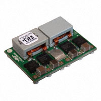
GigaTLynxTM Non-isolated Power Modules: 4.5Vdc – 14Vdc input; 0.7Vdc to 2Vdc, 50A Output
Features
Compliant to RoHS EU Directive 2002/95/EC (-Z versions) Compliant to RoHS EU Directive 2002/95/EC with lead solder exemption (non-Z versions) Input voltage from 4.5Vdc to 14Vdc Output voltage programmable from 0.7 Vdc to 2.0Vdc via external resistor Output current up to 50A Tunable control loop for fast transient response True differential remote sense Negative remote On/Off logic Output voltage sequencing (EZ-SEQUENCE Output over current protection (non-latching) Over temperature protection Monotonic startup under pre-bias conditions Parallel operation with active current sharing Small size and low profile: 33 mm x 22.9 mm x 10 mm (max.) (1.3 in x 0.9 in x 0.393 in (max.))
RTUNE + CO1 CTUNE
Applications
Distributed power architectures Intermediate bus voltage applications Industrial applications Telecommunications equipment
TM
)
Vin+
VIN PGOOD SEQ
+ CI2 CI1
VOUT SENSE+
Vout+
CO2
MODULE
TRIM+
RTrim
Wide operating temperature range [-40°C to 105°C(Ruggedized: -D), 85°C(Regular)] UL* 60950-1, 2 Ed. Recognized, CSA C22.2 No. 60950-1-07 Certified, and VDE‡ (EN60950-1, 2nd Ed.) Licensed ISO** 9001 and ISO 14001 certified manufacturing facilities
nd †
ON/OFF
TRIMGND SENSESENSE-
Description
The GigaTLynxTM series of power modules are non-isolated dc-dc converters that can deliver up to 50A of output current. These modules operate over a wide range of input voltage (VIN = 4.5Vdc-14Vdc) and provide a precisely regulated output voltage from 0.7Vdc to 2.0Vdc, programmable via an external resistor. Features include remote On/Off, adjustable output voltage, over current and over temperature protection, output voltage sequencing and paralleling. The Ruggedized version (-D) is capable of operation up to 105°C and withstand high levels of shock and vibration. The Tunable LoopTM feature, allows the user to optimize the dynamic response of the converter to match the load with reduced amount of output capacitance leading to savings on cost and PWB area.
* UL is a registered trademark of Underwriters Laboratories, Inc.
† ‡
CSA is a registered trademark of Canadian Standards Association. VDE is a trademark of Verband Deutscher Elektrotechniker e.V. ** ISO is a registered trademark of the International Organization of Standards
Document No: DS010-005 ver. 1.23 PDF name: APTS050A0X_ds.pdf
�Data Sheet September 7, 2011
GigaTLynxTM SMT Non-isolated Power Modules: 4.5 – 14Vdc input; 0.7Vdc to 2.0Vdc, 50A Output
Absolute Maximum Ratings
Stresses in excess of the absolute maximum ratings can cause permanent damage to the device. These are absolute stress ratings only, functional operation of the device is not implied at these or any other conditions in excess of those given in the operations sections of the data sheet. Exposure to absolute maximum ratings for extended periods can adversely affect the device reliability.
Parameter Input Voltage Continuous Sequencing pin voltage Operating Ambient Temperature (see Thermal Considerations section) Storage Temperature All All -D version All VsEQ TA TA Tstg -0.3 -40 -40 -55 4 85 105 125 Vdc °C °C °C Device All Symbol VIN Min -0.3 Max 14 Unit Vdc
Electrical Specifications
Unless otherwise indicated, specifications apply over all operating input voltage, resistive load, and temperature conditions.
Parameter Operating Input Voltage Maximum Input Current (VIN= VIN, min to VIN, max, IO=IO, max ) Inrush Transient Input No Load Current (VIN = VIN, nom, Io = 0, module enabled) Input Stand-by Current (VIN = VIN, nom, module disabled) Input Reflected Ripple Current, peak-to-peak (5Hz to 20MHz, 1μH source impedance; VIN, min to VIN, max, IO= IOmax ; See Test configuration section) Input Ripple Rejection (120Hz) All All 50 73 mAp-p dB All VO,set = 0.7Vdc VO,set = 1.8Vdc All It IIN,No load IIN,No load IIN,stand-by 73.4 136 1.3
2
Device Vo,set ≤ 2.0 All
Symbol VIN IIN,max
Min 4.5
Typ ⎯
Max 14 26 1
Unit Vdc Adc As mA mA mA
2
CAUTION: This power module is not internally fused. An input line fuse must always be used.
This power module can be used in a wide variety of applications, ranging from simple standalone operation to an integrated part of sophisticated power architecture. To preserve maximum flexibility, internal fusing is not included; however, to achieve maximum safety and system protection, always use an input line fuse. The safety agencies require a surface mount, fast acting fuse (ie. Littelfuse 456030 series) with a maximum rating of 30 A (see Safety Considerations section). Based on the information provided in this data sheet on inrush energy and maximum dc input current, the same type of fuse with a lower rating can be used. Refer to the fuse manufacturer’s data sheet for further information.
LINEAGE POWER
2
�Data Sheet September 7, 2011
GigaTLynxTM SMT Non-isolated Power Modules: 4.5 – 14Vdc input; 0.7Vdc to 2.0Vdc, 50A Output
Electrical Specifications (continued)
Parameter Output Voltage Set-point (VIN=VIN,nom, IO=IO, nom, Tref=25°C) Output Voltage (Over all operating input voltage, resistive load, and temperature conditions until end of life) Adjustment Range Selected by an external resistor Output Regulation Line (VIN=VIN, min to VIN, max) Load (IO=IO, min to IO, max) Temperature (Tref=TA, min to TA, max) Remote Sense Range Output Ripple and Noise on nominal output (VIN=VIN, nom and IO=IO, min to IO, max Cout = 1μF ceramic//2x10μF ceramic capacitors) Peak-to-Peak (5Hz to 20MHz bandwidth) External Capacitance ESR ≥ 1 mΩ ESR ≥ 10 mΩ With the Tunable Loop ESR ≥ 1 mΩ ESR ≥ 10 mΩ Output Current Output Current Limit Inception (Hiccup Mode ) Output Short-Circuit Current (VO≤250mV) ( Hiccup Mode ) Efficiency VIN= 12V, TA=25°C IO=IO, max , VO= VO,set Switching Frequency VO, set = 0.7Vdc VO,set = 1.2Vdc VO,set = 1.8Vdc All η η η fsw ⎯ 81.1 87.0 90.1 260 ⎯ % % % kHz All All All All All CO, max CO, max Io IO, lim IO, s/c ⎯ ⎯ 0 ⎯ ⎯ 180 5.5 ⎯ ⎯ 20000 20000 50A ⎯ ⎯ μF μF Adc % Io Adc
1 TM
Device All All
Symbol VO, set VO, set
Min -1.0 -2.0
Typ ⎯ ⎯
Max +1.0 +2.0
Unit % VO, set % VO, set
All
VO
0.7
2.0
Vdc
All All All All
⎯ ⎯ ⎯
5 8 8 0.5
mV mV mV Vdc
All
⎯
50
mVpk-pk
Without the Tunable Loop
All All
CO, max CO, max
⎯ ⎯
⎯ ⎯
1200 10000
μF μF
General Specifications
Parameter Telcordia Issue 2, Method I, Case 3, Calculated MTBF (IO=IO, max, TA=40°C) Weight ⎯ Min Typ 4,755,661 14.22 (0.5) Max Unit Hours g (oz.)
__________________________________ External capacitors may require using the new Tunable Loop feature to ensure that the module is stable as well as TM getting the best transient response. See the Tunable Loop section for details.
TM
LINEAGE POWER
3
�Data Sheet September 7, 2011
GigaTLynxTM SMT Non-isolated Power Modules: 4.5 – 14Vdc input; 0.7Vdc to 2.0Vdc, 50A Output
Feature Specifications
Unless otherwise indicated, specifications apply over all operating input voltage, resistive load, and temperature conditions. See Feature Descriptions for additional information.
Parameter On/Off Signal Interface (VIN=VIN, min to VIN, max ; open collector or equivalent, Signal referenced to GND) Logic High (On/Off pin open – Module OFF) Input High Current Input High Voltage Logic Low (Module ON) Input Low Current Input Low Voltage Turn-On Delay and Rise Times (IO=IO, max , VIN = VIN, nom, TA = 25 C, ) Case 1: On/Off input is set to Logic Low (Module ON) and then input power is applied (delay from instant at which VIN =VIN, min until Vo=10% of Vo,set) Case 2: Input power is applied for at least one second and then the On/Off input is set to logic Low (delay from instant at which Von/Off=0.3V until Vo=10% of Vo, set) Output voltage Rise time (time for Vo to rise from 10% of Vo,set to 90% of Vo, set) Output voltage overshoot – Startup IO= IO, max; VIN = 4.5 to 14Vdc, TA = 25 C Over Temperature Protection (See Thermal Consideration section) Sequencing Slew rate capability (VIN, min to VIN, max; IO, min to IO, max VSEQ < Vo) Sequencing Delay time (Delay from VIN, min to application of voltage on SEQ pin) Tracking Accuracy Power-up (2V/ms) Power-down (1V/ms) (VIN, min to VIN, max; IO, min - IO, max VSEQ < Vo) Input Undervoltage Lockout Turn-on Threshold Turn-off Threshold Hysteresis Forced Load Share Accuracy Number of units in Parallel PGOOD (Power Good) Internal pull-up, VPGOOD Overvoltage threshold for PGOOD Undervoltage threshold for PGOOD All All All 5 112.5 87.5 V %VO, set %VO, set All All All All All ⎯ 4.26 4.04 0.22 10 5 V V Vdc % Io All All TsEQ-delay VSEQ –Vo VSEQ –Vo 10 100 200 200 400 msec mV mV All dVSEQ/dt — 2 V/msec All Tref ⎯ 125 ⎯ °C
o o
Device
Symbol
Min
Typ
Max
Unit
All All All All
IIH VIH IIL VIL
0.5 3.0 ⎯ -0.3
⎯ ⎯ ⎯ ⎯
3.3 VIN, max 200 0.6
mA V µA V
All
Tdelay
―
4.8
―
msec
All
Tdelay
―
4.8
―
msec
All
Trise
―
3.6 ―
― 3.0
msec % VO, set
LINEAGE POWER
4
�Data Sheet September 7, 2011
GigaTLynxTM SMT Non-isolated Power Modules: 4.5 – 14Vdc input; 0.7Vdc to 2.0Vdc, 50A Output
Characteristic Curves
The following figures provide typical characteristics for the 12V Giga TLynx
95
TM
50A at 0.7Vo and at 25 C.
o
55 50
90
OUTPUT CURRENT, Io (A)
45 40 35 30 25 20 15 45 55
NC 0.5m/s (100LFM) 1m/s
EFFICIENCY, η (%)
85
Vin=12V Vin=4.5V Vin=14V
80
(200LFM)
Standard Part (85 C) Ruggedized (D) Part (105 C)
1.5m/s (300LFM) 2m/s (400LFM)
75
70 0 10 20 30 40 50
65
75
85
O
95
105
OUTPUT CURRENT, IO (A)
AMBIENT TEMPERATURE, TA C
Figure 1. Converter Efficiency versus Output Current.
OUTPUT VOLTAGE OUTPUT CURRENT
Figure 2. Derating Output Current versus Ambient Temperature and Airflow.
VO (V) (10mV/div) IO (A) (20Adiv)
OUTPUT VOLTAGE
VO (V) (10mV/div)
TIME, t (1μs/div)
TIME, t (0.2ms /div)
Figure 3. Typical output ripple and noise (VIN = 12V, Io = Io,max).
ON/OFF VOLTAGE VON/OFF (V) (5V/div)
Figure 4. Transient Response to Dynamic Load
Change from 50% to 100% at 12Vin, Cext =5x47uF+ +22x330uFpolymer,CTune=330nF,RTune=100ohms
INPUT VOLTAGE OUTPUT VOLTAGE
OUTPUT VOLTAGE
VO (V) (200mV/div)
TIME, t (2ms/div)
VO (V) (200mV/div)
VIN (V) (5V/div)
TIME, t (2ms/div)
Figure 5. Typical Start-up Using On/Off Voltage (Io = Io,max).
Figure 6. Typical Start-up Using Input Voltage (VIN = 12V, Io = Io,max).
LINEAGE POWER
5
�Data Sheet September 7, 2011
GigaTLynxTM SMT Non-isolated Power Modules: 4.5 – 14Vdc input; 0.7Vdc to 2.0Vdc, 50A Output
Characteristic Curves
The following figures provide typical characteristics for the 12V Giga TLynx
95
TM
50A at 1.2 Vo and at 25 C.
o
55 50
90
OUTPUT CURRENT, Io (A)
45 40 35 30 25 20 15 45 55 65 75 85 95
O
EFFICIENCY, η (%)
85
Vin=12V Vin=14V
NC
0.5m/s (100LFM)
80
Vin=4.5V
1m/s (200LFM) 1.5m/s (300LFM) 2m/s (400LFM)
Standard Part (85 C) Ruggedized (D) Part (105 C)
75
70 0 10 20 30 40 50
105
OUTPUT CURRENT, IO (A)
AMBIENT TEMPERATURE, TA C
Figure 7. Converter Efficiency versus Output Current.
OUTPUT VOLTAGE OUTPUT CURRENT,
Figure 8. Derating Output Current versus Ambient Temperature and Airflow.
VO (V) (10mV/div) IO (A) (20Adiv)
OUTPUT VOLTAGE
VO (V) (10mV/div)
TIME, t (1μs/div)
TIME, t (0.1ms /div)
Figure 9. Typical output ripple and noise (VIN = 12V, Io = Io,max).
ON/OFF VOLTAGE
Figure 10. Transient Response to Dynamic Load
Change from 50% to 100% at 12Vin, Cext =5x47uF+ +13x330uFpolymer,CTune=120nF,RTune=180ohms
VON/OFF (V) (5V/div)
INPUT VOLTAGE OUTPUT VOLTAGE
OUTPUT VOLTAGE
VO (V) (500mV/div)
TIME, t (2 ms/div)
VO (V) (500mV/div)
VIN (V) (5V/div)
TIME, t (2 ms/div)
Figure 11. Typical Start-up Using On/Off Voltage (Io = Io,max). LINEAGE POWER
Figure 12. Typical Start-up Using Input Voltage (VIN = 12V, Io = Io,max). 6
�Data Sheet September 7, 2011
GigaTLynxTM SMT Non-isolated Power Modules: 4.5 – 14Vdc input; 0.7Vdc to 2.0Vdc, 50A Output
Characteristic Curves
The following figures provide typical characteristics for the 12V Giga TLynx
100 95
TM
50A at 1.8 Vo and at 25 C.
o
Vin=12V
55 50 45
OUTPUT CURRENT, Io (A)
Output Voltage set to 2V for thermal derating curve
EFFICIENCY, η (%)
90 85 80 75 70 0 10 20 30 40 50
Vin=4.5V
40 35 30 25 20 15 10 35
NC 0.5m/s (100LFM) 1m/s (200LFM) 1.5m/s
Vin=14V
Standard Part (300LFM) (85 C) Ruggedized (D) Part (105 C)
2m/s (400LFM)
45
55
65
75
85
95
O
105
OUTPUT CURRENT, IO (A)
AMBIENT TEMPERATURE, TA C
Figure 13. Converter Efficiency versus Output Current.
Figure 14. Derating Output Current versus Ambient Temperature and Airflow.
OUTPUT VOLTAGE OUTPUT CURRENT,
OUTPUT VOLTAGE
VO (V) (10mV/div)
TIME, t (1μs/div)
IO (A) (20Adiv)
VO (V) (20mV/div)
TIME, t (0.1ms /div)
Figure 15. Typical output ripple and noise (VIN = 12V, Io = Io,max).
Figure 16. Transient Response to Dynamic Load
Change from 50% to 100% at 12Vin, Cext =5x47uF+ +8x330uFpolymer,CTune=47nF,RTune=220ohms
ON/OFF VOLTAGE
VON/OFF (V) (5V/div)
INPUT VOLTAGE OUTPUT VOLTAGE
OUTPUT VOLTAGE
VO(V) (500mV/div)
TIME, t (2 ms/div)
VO (V) (500mV/div)
VIN (V) (5V/div)
TIME, t (2 ms/div)
Figure 17. Typical Start-up Using On/Off Voltage (Io = Io,max). LINEAGE POWER
Figure 18. Typical Start-up Using Input Voltage (VIN = 12V, Io = Io,max). 7
�Data Sheet September 7, 2011
GigaTLynxTM SMT Non-isolated Power Modules: 4.5 – 14Vdc input; 0.7Vdc to 2.0Vdc, 50A Output
Test Configurations
TO OSCILLOSCOPE LTEST 1 μH VIN(+) CURRENT PROBE
Design Considerations
Input Filtering
The Giga TLynx module should be connected to a low ac-impedance source. A highly inductive source can affect the stability of the module. An input capacitance must be placed directly adjacent to the input pin of the module, to minimize input ripple voltage and ensure module stability. To minimize input voltage ripple, ceramic capacitors are recommended at the input of the module. Figure 22 shows the input ripple voltage for various output voltages at maximum load current with 2x22 µF or 4x22 µF or 4x47 µF ceramic capacitors and an input of 12V.
250
TM
BATTERY
CS 1000μF Electrolytic E.S.R.