LT1767/LT1767-1.8/
LT1767-2.5/LT1767-3.3/LT1767-5
Monolithic 1.5A, 1.25MHz
Step-Down Switching Regulators
Features
n
n
n
n
n
n
n
n
n
n
n
n
n
Description
1.5A Switch in a Small MSOP Package
Constant 1.25MHz Switching Frequency
High Power Exposed Pad (MS8E) Package
Wide Operating Voltage Range: 3V to 25V
High Efficiency 0.22Ω Switch
1.2V Feedback Reference Voltage
Fixed Output Voltages of 1.8V, 2.5V, 3.3V, 5V
2% Overall Output Tolerance
Uses Low Profile Surface Mount Components
Low Shutdown Current: 6µA
Synchronizable to 2MHz
Current Mode Loop Control
Constant Maximum Switch Current Rating at All Duty
Cycles*
Applications
n
n
n
n
n
The LT®1767 is a 1.25MHz monolithic buck switching
regulator. A high efficiency 1.5A, 0.22Ω switch is included
on the die together with all the control circuitry required
to complete a high frequency, current mode switching
regulator. Current mode control provides fast transient
response and excellent loop stability.
New design techniques achieve high efficiency at high
switching frequencies over a wide operating range. A
low dropout internal regulator maintains consistent performance over a wide range of inputs from 24V systems
to Li-Ion batteries. An operating supply current of 1mA
improves efficiency, especially at lower output currents.
Shutdown reduces quiescent current to 6µA. Maximum
switch current remains constant at all duty cycles. Synchronization allows an external logic level signal to increase
the internal oscillator from 1.5MHz to 2MHz.
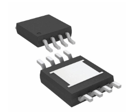
The LT1767 is available in an 8-pin MSOP fused lead-frame
package and a low thermal resistance exposed pad package.
Full cycle-by-cycle current limit and thermal shutdown are
provided. High frequency operation allows the reduction
of input and output filtering components and permits the
use of chip inductors.
DSL Modems
Portable Computers
Wall Adapters
Battery-Powered Systems
Distributed Power
L, LT, LTC, LTM, Linear Technology, the Linear logo and Burst Mode are registered trademarks
of Linear Technology Corporation. All other trademarks are the property of their respective
owners. Protected by U.S. Patents, including 6611131, 6498466.
Typical Application
Efficiency vs Load Current
12V to 3.3V Step-Down Converter
95
D2
CMDSH-3
VIN
12V
C3
2.2µF
CERAMIC
BOOST
VIN
OPEN
OR
HIGH
= ON
L1
5µH
VSW
LT1767-3.3
SHDN
SYNC
OUTPUT
3.3V
1.2A*
FB
GND
VC
CC
1.5nF
RC
4.7k
D1
UPS120
C1
10µF
CERAMIC
EFFICIENCY (%)
C2
0.1µF
85
80
75
70
*MAXIMUM OUTPUT CURRENT IS SUBJECT TO THERMAL DERATING.
VIN = 10V
VOUT = 5V
90
1767 TA01
0
0.2
0.4 0.6 0.8
1
LOAD CURRENT (A)
1.2
1.4
1767 TA01a
1767fb
For more information www.linear.com/LT1767
1
�LT1767/LT1767-1.8/
LT1767-2.5/LT1767-3.3/LT1767-5
Absolute Maximum Ratings
(Note 1)
Input Voltage ............................................................ 25V
BOOST Pin Above SW .............................................. 20V
Max BOOST Pin Voltage.............................................35V
SHDN Pin.................................................................. 25V
FB Pin Voltage ............................................................ 6V
FB Pin Current.......................................................... 1mA
SYNC Pin Current ................................................... 1mA
Operating Junction Temperature Range (Note 2)
LT1767E ............................................ – 40°C to 125°C
Storage Temperature Range .................. –65°C to 150°C
Lead Temperature (Soldering, 10 sec) ................. 300°C
Pin Configuration
TOP VIEW
BOOST
VIN
SW
GND
1
2
3
4
TOP VIEW
8
7
6
5
BOOST
VIN
SW
GND
SYNC
VC
FB
SHDN
MS8 PACKAGE
8-LEAD PLASTIC MSOP
1
2
3
4
8
7
6
5
SYNC
VC
FB
SHDN
MS8E PACKAGE
8-LEAD PLASTIC MSOP
TJMAX = 125°C, θJA = 110°C/W
GROUND PIN CONNECTED TO LARGE COPPER AREA
TJMAX = 125°C, θJA = 40°C/W
GROUND PIN CONNECTED TO LARGE COPPER AREA ON PCB
Order Information
LEAD FREE FINISH
TAPE AND REEL
PART MARKING
PACKAGE DESCRIPTION
TEMPERATURE RANGE
LT1767EMS8#PBF
LT1767EMS8-1.8#PBF
LT1767EMS8#TRPBF
LTLS
8-Lead Plastic MSOP
–40°C to 125°C
LT1767EMS8-1.8#TRPBF
LTWG
8-Lead Plastic MSOP
–40°C to 125°C
LT1767EMS8-2.5#PBF
LT1767EMS8-2.5#TRPBF
LTWD
8-Lead Plastic MSOP
–40°C to 125°C
LT1767EMS8-3.3#PBF
LT1767EMS8-3.3#TRPBF
LTWE
8-Lead Plastic MSOP
–40°C to 125°C
LT1767EMS8-5#PBF
LT1767EMS8-5#TRPBF
LTWF
8-Lead Plastic MSOP
–40°C to 125°C
LT1767EMS8E#PBF
LT1767EMS8E#TRPBF
LTZG
8-Lead Plastic MSOP, Exposed Pad
–40°C to 125°C
LT1767EMS8E-1.8#PBF
LT1767EMS8E-1.8#TRPBF
LTZH
8-Lead Plastic MSOP, Exposed Pad
–40°C to 125°C
LT1767EMS8E-2.5#PBF
LT1767EMS8E-2.5#TRPBF
LTZJ
8-Lead Plastic MSOP, Exposed Pad
–40°C to 125°C
LT1767EMS8E-3.3#PBF
LT1767EMS8E-3.3#TRPBF
LTZK
8-Lead Plastic MSOP, Exposed Pad
–40°C to 125°C
LT1767EMS8E-5#PBF
LT1767EMS8E-5#TRPBF
LTZL
8-Lead Plastic MSOP, Exposed Pad
–40°C to 125°C
Consult LTC Marketing for parts specified with wider operating temperature ranges.
Consult LTC Marketing for information on nonstandard lead based finish parts.
For more information on lead free part marking, go to: http://www.linear.com/leadfree/
For more information on tape and reel specifications, go to: http://www.linear.com/tapeandreel/
2
1767fb
For more information www.linear.com/LT1767
�LT1767/LT1767-1.8/
LT1767-2.5/LT1767-3.3/LT1767-5
Electrical Characteristics The l denotes the specifications which apply over the full operating
temperature range, otherwise specifications are at TA = 25°C. VIN = 15V, VC = 0.8V, Boost = VIN + 5V, SHDN, SYNC and switch open
unless otherwise noted.
PARAMETER
CONDITIONS
MIN
TYP
MAX
Maximum Switch Current Limit
TA = 0°C to 125°C
TA = < 0°C
1.5
1.3
2
3
3
Oscillator Frequency
3.3V < VIN < 25V
1.1
1.1
1.25
1.4
1.5
MHz
MHz
330
400
500
mV
mV
2.6
2.73
V
1
1.3
mA
6
20
45
µA
µA
l
Switch On Voltage Drop
ISW = –1.5A, 0°C ≤ TA ≤ 125°C and –1.3A, TA < 0°C
l
VIN Undervoltage Lockout
(Note 3)
l
VIN Supply Current
VFB = VNOM + 17%
l
Shutdown Supply Current
VSHDN = 0V, VIN = 25V, VSW = 0V
2.47
l
Feedback Voltage
3V < VIN < 25V, 0.4V < VC < 0.9V LT1767 (Adj)
(Note 3)
1.182
1.176
1.2
1.218
1.224
V
V
LT1767-1.8
l
1.764
1.8
1.836
V
LT1767-2.5
l
2.45
2.5
2.55
V
LT1767-3.3
l
3.234
3.3
3.366
V
LT1767-5
l
4.9
5
5.1
V
–0.25
–0.5
µA
10.5
14.7
19
29
15
21
27.5
42
21
30
39
60
kΩ
kΩ
kΩ
kΩ
150
350
l
500
850
1300
µMho
VFB = VNOM – 17%
l
80
120
160
µA
VFB = VNOM + 17%
l
70
110
180
µA
FB Input Current
LT1767 (Adj)
l
LT1767-1.8
LT1767-2.5
LT1767-3.3
LT1767-5
l
l
l
l
Error Amp Voltage Gain
0.4V < VC < 0.9V
Error Amp Transconductance
∆IVC = ±10µA
VC Pin Source Current
VC Pin Sink Current
VC Pin to Switch Current Transconductance
Duty Cycle = 0%
VC Pin 1.5A ISW Threshold
Maximum Switch Duty Cycle
A
A
l
FB Input Resistance
VC Pin Minimum Switching Threshold
UNITS
VC = 1.2V, ISW = 400mA
l
85
80
2.5
A/V
0.35
V
0.9
V
90
%
%
Minimum Boost Voltage Above Switch
ISW = –1.5A, 0°C ≤ TA ≤ 125°C and –1.3A, TA < 0°C
l
1.8
2.7
V
Boost Current
ISW = – 0.5A (Note 4)
ISW = –1.5A, 0°C ≤ TA ≤ 125°C and –1.3A, TA < 0°C (Note 4)
l
l
10
30
15
45
mA
mA
1.27
1.33
1.40
V
SHDN Input Current (Shutting Down)
SHDN = 60mV Above Threshold
l
–7
–10
–13
µA
SHDN Threshold Current Hysteresis
SHDN = 100mV Below Threshold
l
4
7
10
µA
1.5
2.2
V
SHDN Threshold Voltage
l
SYNC Threshold Voltage
SYNC Input Frequency
SYNC Pin Resistance
1.5
ISYNC = 1mA
2
20
MHz
kΩ
1767fb
For more information www.linear.com/LT1767
3
�LT1767/LT1767-1.8/
LT1767-2.5/LT1767-3.3/LT1767-5
Electrical Characteristics
Note 3: Minimum input voltage is defined as the voltage where the internal
regulator enters lockout. Actual minimum input voltage to maintain a
regulated output will depend on output voltage and load current. See
Applications Information.
Note 4: Current flows into the BOOST pin only during the on period of the
switch cycle.
Note 1: Stresses beyond those listed under Absolute Maximum Ratings
may cause permanent damage to the device. Exposure to any Absolute
Maximum Rating condition for extended periods may affect device
reliability and lifetime.
Note 2: The LT1767E is guaranteed to meet performance specifications
from 0°C to 125°C. Specifications over the – 40°C to 125°C operating
junction temperature range are assured by design, characterization and
correlation with statistical process controls.
TYPICAL PERFORMANCE Characteristics
FB vs Temperature (Adj)
Switch On Voltage Drop
1.22
Oscillator Frequency
400
1.20
1.19
1.18
–50
–25
0
25
50
75
TEMPERATURE (°C)
100
25°C
300
1.40
250
–40°C
200
150
1.35
1.30
1.25
100
1.20
50
1.15
0
125
1.45
FREQUENCY (MHz)
SWITCH VOLTAGE (mV)
1.21
1.50
125°C
350
FB VOLTAGE (V)
TA = 25°C, unless otherwise noted.
1
0.5
SWITCH CURRENT (A)
0
1767 G01
1.10
–50
1.5
–25
1767 G02
0
25
50
75
TEMPERATURE (°C)
100
125
1767 G03
SHDN Threshold vs Temperature
SHDN Supply Current vs VIN
SHDN = 0V
1.34
1.32
–10
SHUTTING DOWN
5
SHDN INPUT (µA)
VIN CURRENT (µA)
SHDN THRESHOLD (V)
1.36
4
3
2
–25
0
25
50
75
TEMPERATURE (°C)
100
125
0
–8
–6
–4
STARTING UP
–2
1
1767 G04
4
–12
6
1.38
1.30
–50
SHDN IP Current vs Temperature
7
1.40
0
5
10
15
VIN (V)
20
25
30
1767 G05
0
–50
–25
0
25
50
75
TEMPERATURE (°C)
100
125
1767 G06
1767fb
For more information www.linear.com/LT1767
�LT1767/LT1767-1.8/
LT1767-2.5/LT1767-3.3/LT1767-5
TYPICAL PERFORMANCE Characteristics
Minimum
Minimum Input
Input Voltage,
Voltage, 3.3V
3.3V Out
Out
SHDN Supply Current
VIN = 15V
5.5
VIN CURRENT (µA)
INPUT VOLTAGE (V)
6.0
TO START
5.0
4.5
4.0
3.5
2.5
1
250
1000
200
800
150
100
10
100
LOAD CURRENT (mA)
0
1k
MINIMUM
INPUT
VOLTAGE
600
400
200
50
TO RUN
3.0
1200
300
BOOST DIODE TIED TO VOUT
BOOST DIODE TIED TO VIN
6.5
Input Supply Current
VIN CURRENT (µA)
7.0
TA = 25°C, unless otherwise noted.
0.2
0
1767 G07
0.4 0.6 0.8
1
1.2
SHUTDOWN VOLTAGE (V)
0
1.4
0
5
10
15
20
INPUT VOLTAGE (V)
25
1767 G08
30
SWITCH CURRENT
1.0
20
0.5
10
FB CURRENT
0
0.2
0.4
0.6
0.8
FEEDBACK VOLTAGE (V)
1.5
1.3
L = 4.7µH
OUTPUT CURRENT (A)
1.5
Maximum Load Current,
VOUT = 2.5V
1.5
OUTPUT CURRENT (A)
SWITCH PEAK CURRENT (A)
40
FB INPUT CURRENT (µA)
2.0
0
1767 G09
Maximum Load Current,
VOUT = 5V
Current Limit Foldback
30
1.1
0.9
L = 2.2µH
0.7
L = 4.7µH
1.3
L = 2.2µH
1.1
L = 1.5µH
0.9
L = 1.5µH
1
0
1.2
1767 G10
0.5
0
5
10
15
INPUT VOLTAGE (V)
20
25
1767 G11
0.7
0
5
10
15
INPUT VOLTAGE (V)
20
25
1767 G12
1767fb
For more information www.linear.com/LT1767
5
�LT1767/LT1767-1.8/
LT1767-2.5/LT1767-3.3/LT1767-5
PIN FUNCTIONS
FB: The feedback pin is used to set output voltage using
an external voltage divider that generates 1.2V at the pin
with the desired output voltage. The fixed voltage 1.8V,
2.5V, 3.3V and 5V versions have the divider network included internally and the FB pin is connected directly to
the output. If required, the current limit can be reduced
during start up or short-circuit when the FB pin is below
0.5V (see the Current Limit Foldback graph in the Typical
Performance Characteristics section). An impedance of
less than 5kΩ (adjustable part only) at the FB pin is needed
for this feature to operate.
and the GND pin short. The GND pin of the MS8 package
is directly attached to the internal tab. This pin should
be attached to a large copper area to improve thermal
resistance. The exposed pad of the MS8E package is also
connected to GND. This should be soldered to a large
copper area to improve its thermal resistance.
BOOST: The BOOST pin is used to provide a drive voltage,
higher than the input voltage, to the internal bipolar NPN
power switch. Without this added voltage, the typical
switch voltage loss would be about 1.5V. The additional
boost voltage allows the switch to saturate and voltage
loss approximates that of a 0.22Ω FET structure.
SYNC: The sync pin is used to synchronize the internal
oscillator to an external signal. It is directly logic compatible and can be driven with any signal between 20% and
80% duty cycle. The synchronizing range is equal to initial
operating frequency, up to 2MHz. See Synchronization in
Applications Information section for details. When not in
use, this pin should be grounded.
VIN: This is the collector of the on-chip power NPN switch.
This pin powers the internal circuitry and internal regulator. At NPN switch on and off, high dI/dt edges occur
on this pin. Keep the external bypass capacitor and catch
diode close to this pin. All trace inductance in this path
will create a voltage spike at switch off, adding to the VCE
voltage across the internal NPN.
GND: The GND pin acts as the reference for the regulated
output, so load regulation will suffer if the “ground” end of
the load is not at the same voltage as the GND pin of the
IC. This condition will occur when load current or other
currents flow through metal paths between the GND pin
and the load ground point. Keep the ground path short
between the GND pin and the load and use a ground plane
when possible. Keep the path between the input bypass
6
VSW: The switch pin is the emitter of the on-chip power
NPN switch. This pin is driven up to the input pin voltage
during switch on time. Inductor current drives the switch
pin negative during switch off time. Negative voltage must
be clamped with an external catch diode with a VBR