LT5537
Wide Dynamic Range
RF/IF Log Detector
DESCRIPTIO
U
FEATURES
■
■
■
■
■
■
■
Low Frequency to 1000MHz Operation
83dB Dynamic Range with ±1dB Nonlinearity
at 200MHz
Sensitivity –76dBm or Better at 200MHz
Log-Linear Transfer Slope of 20mV/dB
Supply Voltage Range: 2.7V to 5.25V
Supply Current: 13.5mA at 3V
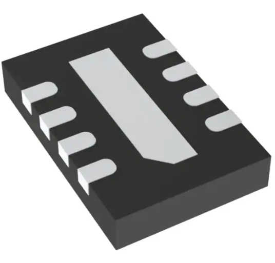
Tiny 8-Lead (3mm × 2mm) DFN Package
U
APPLICATIO S
■
■
■
■
■
■
■
The LT®5537 is a wide dynamic range RF/IF detector,
operational from below 10MHz to 1000MHz. The lower
limit of the operating frequency range can be extended to
near DC by the use of an external capacitor. The input
dynamic range at 200MHz with ±3dB nonlinearity is 90dB
(from –76dBm to 14dBm, single-ended 50Ω input). The
detector output voltage slope is nominally 20mV/dB, and
the typical temperature coefficient is 0.01dB/°C at 200MHz.
, LTC and LT are registered trademarks of Linear Technology Corporation.
All other trademarks are the property of their respective owners.
Linear-to-Log Signal Level Conversion
Received Signal Strength Indication (RSSI)
RF Power Control
RF/IF Power Detection
Receiver RF/IF Gain Control
Envelope Detection
ASK Receiver
U
TYPICAL APPLICATIO
OPTIONAL
4
Output Voltage, Linearity Error
vs Input Power at 200MHz
5
CAP+
7k
CAP–
7k
2.4
OFFSET
CANCELLATION
IN
IN
–
15nF
3
2.0
6
1nF
2
85°C
1µF
25°C
1.6
VOUT (V)
2
+
3
1.2
1
–40°C
0
0.8
OUTPUT
BUFFER
DETECTOR CELLS
1
ENBL
BANDGAP REFERENCE
AND BIASING
OUT
7.2k
VEE
0.4
–2
8
VCC = ENBL = 3V
7
0
–80
–60
–40
–20
0
INPUT POWER (dBm)
–3
20
5537 TA01b
EXPOSED PAD
9
–1
LINEARITY ERROR (dB)
15nF
RF IN
VCC
5537 TA01a
5537fa
1
�LT5537
W W
W
AXI U
U
ABSOLUTE
RATI GS
U
U
W
PACKAGE/ORDER I FOR ATIO
(Note 1)
Power Supply Voltage ........................................... 5.5V
Enable Voltage ................................... –0.2V, VCC + 0.2V
Input Power (Note 2) ......................................... 22dBm
Operating Ambient Temperature Range .. – 40°C to 85°C
Storage Temperature Range ................ – 65°C to 125°C
Maximum Junction Temperature ......................... 125°C
TOP VIEW
ENBL 1
8
OUT
IN+ 2
7
VEE
6
VCC
5
CAP–
IN– 3
9
CAP+ 4
DDB PACKAGE
8-LEAD (3mm ´ 2mm) PLASTIC DFN
θJA = 76°C/W
EXPOSED PAD (PIN 9) SHOULD BE SOLDERED TO PCB
DDB PART MARKING
LBJR
ORDER PART NUMBER
LT5537EDDB
Order Options Tape and Reel: Add #TR
Lead Free: Add #PBF Lead Free Tape and Reel: Add #TRPBF
Lead Free Part Marking: http://www.linear.com/leadfree/
Consult LTC Marketing for parts specified with wider operating temperature ranges.
ELECTRICAL CHARACTERISTICS
PARAMETER
VCC = 3V, ENBL = 3V, TA = 25°C, unless otherwise specified. (Notes 3, 4)
CONDITIONS
MIN
TYP
MAX
UNITS
Signal Input
Input Frequency Range
(Note 5)
Maximum Input Power for Monotonic Output
50Ω Termination
200MHz
600MHz
1GHz
DC Common Mode Voltage
Small-Signal Impedance
10 to 1000
MHz
14.0
11.6
9.4
dBm
dBm
dBm
VCC – 0.4
Measured at 200MHz
V
1.73kΩ //1.45pF
f = 10MHz
Linear Dynamic Range
±3dB Error
±1dB Error
88.8
72.5
dB
dB
Slope
R1 = 33k (Note 8)
19.6
mV/dB
Intercept
VOUT = 0V, Extrapolated
–97
dBm
Sensitivity
(Notes 3, 7)
–76.7
dBm
Temperature Coefficient
PIN = –20dBm
–0.007
dB/°C
f = 50MHz
Linear Dynamic Range
±3dB Error
±1dB Error
Slope
R1 = 33k (Note 8)
Intercept
VOUT = 0V, Extrapolated
–96
dBm
Sensitivity
(Notes 3, 7)
–77.2
dBm
Temperature Coefficient
PIN = –20dBm
–0.005
dB/°C
90.6
81.0
20
dB
dB
mV/dB
5537fa
2
�LT5537
ELECTRICAL CHARACTERISTICS
VCC = 3V, ENBL = 3V, TA = 25°C, unless otherwise specified. (Notes 3, 4)
PARAMETER
f = 100MHz
CONDITIONS
MIN
TYP
MAX
UNITS
Linear Dynamic Range
±3dB Error
±1dB Error
90.5
82.8
dB
dB
Slope
R1 = 33k (Note 8)
20.3
mV/dB
Intercept
VOUT = 0V, Extrapolated
–95
dBm
Sensitivity
(Notes 3, 7)
–77
dBm
Temperature Coefficient
PIN = –20dBm
–0.004
dB/°C
f = 200MHz
Linear Dynamic Range
±3dB Error
±1dB Error
90.3
83.5
dB
dB
Slope
R1 = 33k (Note 8)
21.2
mV/dB
Intercept
VOUT = 0V, Extrapolated
–94
dBm
Sensitivity
(Notes 3, 7)
–76.4
dBm
Temperature Coefficient
PIN = –20dBm
0.010
dB/°C
Linear Dynamic Range
±3dB Error
±1dB Error
88.2
70.8
dB
dB
Slope
R1 = 33k (Note 8)
23.1
mV/dB
Intercept
VOUT = 0V, Extrapolated
–91
dBm
f = 400MHz
Sensitivity
(Notes 3, 7)
–75.3
dBm
Temperature Coefficient
PIN = –20dBm
0.019
dB/°C
Linear Dynamic Range
±3dB Error
±1dB Error
85.8
72.5
dB
dB
Slope
R1 = 33k (Note 8)
25.2
mV/dB
Intercept
VOUT = 0V, Extrapolated
–89
dBm
Sensitivity
(Notes 3, 7)
–74.1
dBm
Temperature Coefficient
PIN = –20dBm
0.026
dB/°C
Linear Dynamic Range
±3dB Error
±1dB Error
63.5
51.7
dB
dB
Slope
R1 = 33k (Note 8)
31.4
mV/dB
Intercept
VOUT = 0V, Extrapolated
–80
dBm
Sensitivity
(Notes 3, 7)
–69.2
dBm
Temperature Coefficient
PIN = –20dBm
0.031
dB/°C
f = 600MHz
f = 1GHz
Output
Starting Voltage
No RF Signal Present
0.4
Response Time
Input from –30dBm to 0dBm, CLOAD = 2.5pF
110
Baseband Modulation Bandwidth
Output Load Capacitance = 2.5pF
V
ns
6
MHz
Shutdown Mode
ENBL = High (On)
1
V
ENBL = Low (Off)
0.3
V
100
0
µA
µA
Turn-On Time
100
µs
Turn-Off Time
100
µs
ENBL Input Current
VENBL = 3V
VENBL = 0V
5537fa
3
�LT5537
ELECTRICAL CHARACTERISTICS
VCC = 3V, ENBL = 3V, TA = 25°C, unless otherwise specified. (Notes 3, 4)
PARAMETER
Power Supply
CONDITIONS
MIN
Supply Voltage
(Note 6)
2.7
Supply Current
VCC = 3V
10
Shutdown Current
ENBL = Low
Note 1: Stresses beyond those listed under Absolute Maximum Ratings
may cause permanent damage to the device. Exposure to any Absolute
Maximum Rating condition for extended periods may affect device
reliability and lifetime.
Note 2: Maximum differential AC input voltage between IN+ and IN– is 4V
peak. Equivalent to 22dBm with 50Ω input impedance or 16dBm with
200Ω input impedance (1:4 transformer used).
Note 3: Tests are performed as shown in the configuration of Figure 13.
Note 4: Specifications over the –40°C to 85°C temperature range are
assured by design, characterization and correlation with statistical process
control.
Note 5: Operation at lower frequency is possible as described in the “Low
Frequency Operation” section in Applications Information.
TYP
MAX
5.25
13.5
15
UNITS
V
mA
µA
500
Note 6: The maximum output voltage is limited to approximately VCC –
0.6V. Either the output slope should be reduced or input power level
should be limited in order to avoid saturating the output circuit when VCC <
3V. See discussion in “Dynamic Range” section.
Note 7: Sensitivity is defined as the minimum input power required for the
output voltage to be within 3dB of the ideal log-linear transfer curve.
Sensitivity can be improved by as much as 10dB by using a narrowband
input impedance transformation network. See discussion in “Input
Matching” section.
Note 8: The output slope is adjustable using an external pull-down resistor
(R1). See Applications Information for description of the output circuit.
U W
TYPICAL PERFOR A CE CHARACTERISTICS
ENBL Current vs Supply Voltage
Supply Current vs Supply Voltage
20
250
RF INPUT SIGNAL OFF
ENBL = VCC
TA = 85°C
ENBL CURRENT (µA)
SUPPLY CURRENT (mA)
18
16
TA = 25°C
14
200
TA = 85°C
150
TA = 25°C
TA = –40°C
100
TA = –40°C
12
10
RF INPUT SIGNAL OFF
ENBL = VCC
50
2.5
3.0
3.5
4.0
4.5
SUPPLY VOLTAGE (V)
5.0
5.5
5537 G02
2.5
3.0
3.5
4.0
4.5
SUPPLY VOLTAGE (V)
5.0
5.5
5537 G03
5537fa
4
�LT5537
U W
TYPICAL PERFOR A CE CHARACTERISTICS
Output Voltage, Linearity Error
vs Input Power at 10MHz
2.0
3
3
2
2
–40°C
2.0
1
0
1.2
0
0.8
–1
0.4
–2
–2
–3
–3
–80
0
–80
–60
20
–40
–20
0
INPUT POWER (dBm)
85°C
–1
–60
VCC = ENBL = 3V
25°C
VOUT (V)
1.6
0
–40°C
–2
1.2
2
0
1
0
–2
–3
–3
–80
–60
–40
–20
0
INPUT POWER (dBm)
20
–1
–40°C
2.0
2
2
0
0.8
–1
0.4
VCC = ENBL = 3V
20
5537 G10
Typical Detector Characteristics
2.4
NORMALIZED AT 25°C
VCC = ENBL = 3V
2.0
TA = 25°C
200MHz
ENBL = VCC
85°C
1.6
1
VOUT (V)
–40°C
LINEARITY ERROR (dB)
1
VOUT VARIATION (dB)
3
20
–40
–20
0
INPUT POWER (dBm)
5537 G09
VOUT Variation vs Input Power
at 200MHz
25°C
–60
5537 G08
3
–40
–20
0
INPUT POWER (dBm)
85°C
–2
0
–80
85°C
VOUT (V)
2
0.4
20
–40
–20
0
INPUT POWER (dBm)
20
–40
–20
0
INPUT POWER (dBm)
NORMALIZED AT 25°C
VCC = ENBL = 3V
–1
2.4
–60
–3
–60
0.8
Output Voltage, Linearity Error
vs Input Power at 200MHz
0
–80
–2
3
1
–40°C
5537 G07
1.2
0.4
3
85°C
1
1.6
–1
VOUT Variation vs Input Power
at 100MHz
2.0
–60
0.8
5537 G06
LINEARITY ERROR (dB)
VOUT VARIATION (dB)
2.4
85°C
–3
–80
0
–40°C
Output Voltage, Linearity Error
vs Input Power at 100MHz
NORMALIZED AT 25°C
VCC = ENBL = 3V
–1
1.2
1
5537 G05
VOUT Variation vs Input Power
at 50MHz
2
25°C
0
–80
20
–40
–20
0
INPUT POWER (dBm)
5537 G04
3
2
1.6
–40°C
VOUT VARIATION (dB)
VOUT (V)
1
85°C
3
VCC = ENBL = 3V
LINEARITY ERROR (dB)
1.6
2.4
NORMALIZED AT 25°C
VCC = ENBL = 3V
85°C
LINEARITY ERROR (dB)
25°C
Output Voltage, Linearity Error
vs Input Power at 50MHz
VOUT (V)
VCC = ENBL = 3V
VOUT VARIATION (dB)
2.4
VOUT Variation vs Input Power
at 10MHz
0
–1
5V
1.2
3V
0.8
–40°C
–2
–2
–3
–3
–80
0.4
–60
–40
–20
0
INPUT POWER (dBm)
20
5537 G11
0
–80
–60
–20
–40
INPUT POWER (dBm)
0
20
5537 G12
5537fa
5
�LT5537
U W
TYPICAL PERFOR A CE CHARACTERISTICS
Output Voltage, Linearity Error
vs Input Power at 400MHz
3
2
2
–40°C
0
1.0
–1
0.5
VCC = ENBL = 3V
0
–80
–60
–40
–20
0
INPUT POWER (dBm)
25°C
2.0
0
–1
–2
–3
–3
–80
–60
1
VOUT (V)
–1
85°C
25°C
1.5
3
3
2
2
1
0
–40°C
20
85°C
1
0
–1
–1
0.5
–2
–2
–3
–3
–80
VCC = ENBL = 3V
0
–80
–60
–40
–20
0
INPUT POWER (dBm)
5537 G16
–3
20
NORMALIZED AT 25°C
VCC = ENBL = 3V
1.0
–40°C
–2
20
–40°C
5537 G17
–60
20
–40
–20
0
INPUT POWER (dBm)
5537 G18
Output Voltage Distribution vs Temperature at –20dBm
Output Voltage Distribution vs Temperature at –50dBm
25
25
RF PIN = –50dBm at 200MHz
VCC = ENBL = 3V
RF PIN = –20dBm at 200MHz
VCC = ENBL = 3V
25°C
–40°C
85°C
20
DISTRIBUTION (%)
20
DISTRIBUTION (%)
–2
VOUT Variation vs Input Power
at 1GHz
2.0
–40
–20
0
INPUT POWER (dBm)
0.5
5537 G15
LINEARITY ERROR (dB)
VOUT VARIATION (dB)
2.5
85°C
–60
–1
VCC = ENBL = 3V
0
–80
–60
–40
–20
0
INPUT POWER (dBm)
20
–40
–20
0
INPUT POWER (dBm)
3.0
0
0
1.0
Output Voltage, Linearity Error
vs Input Power at 1GHz
NORMALIZED AT 25°C
VCC = ENBL = 3V
–3
–80
–40°C
5537 G11
VOUT Variation vs Input Power
at 600MHz
2
1.5
1
–40°C
5537 G13
3
2
85°C
1
–2
20
2.5
85°C
VOUT VARIATION (dB)
VOUT (V)
1
3
LINEARITY ERROR (dB)
25°C
2.0
LINEARITY ERROR (dB)
85°C
3.0
NORMALIZED AT 25°C
VCC = ENBL = 3V
VOUT (V)
2.5
3
VOUT VARIATION (dB)
3.0
1.5
Output Voltage, Linearity Error
vs Input Power at 600MHz
VOUT Variation vs Input Power
at 400MHz
15
10
25°C
–40°C
85°C
15
10
5
5
0
0
0.8 0.825 0.85 0.875 0.9 0.925 0.95 0.975 1
OUTPUT VOLTAGE (V)
1.025 1.05 1.075 1.1
5537 G19
1.45 1.475 1.5 1.525 1.55 1.575 1.6 1.625 1.65 1.675 1.7 1.725 1.75
5537 G20
OUTPUT VOLTAGE (V)
5537fa
6
�LT5537
U
U
U
PI FU CTIO S
ENBL (Pin 1): Enable Pin. When the input voltage is higher
than 1V, the circuit is ON. When the input voltage is less than
0.3V, or this pin is not connected, the chip is disabled (OFF).
VCC (Pin 6): Power Supply Pin. This pin should be decoupled
using 1000pF and 0.1µF capacitors.
VEE (Pin 7): Ground pin.
IN+, IN– (Pins 2, 3): Differential Signal Input Pins. These
pins are internally biased to VCC – 0.4V. The impedance
between IN+ and IN– is approximately 1.73kΩ//1.45pF at
200MHz. The input pins should be AC coupled.
OUT (Pin 8): Output pin.
Exposed Pad (Pin 9): Should be connected to PCB ground.
CAP+, CAP– (Pins 4, 5): External Filter Capacitor Pins. The
minimum RF input frequency can be lowered by adding an
optional external capacitor between CAP+ and CAP–.
W
BLOCK DIAGRA
7k
4
5
CAP+
CAP–
7k
VCC
OFFSET
CANCELLATION
2
3
IN
IN –
OUTPUT
BUFFER
DETECTOR CELLS
OUT
7.2k
VEE
1
6
+
ENBL
BANDGAP REFERENCE
AND BIASING
8
7
EXPOSED PAD
7
5537 BD
5537fa
7
�LT5537
U
W
U U
APPLICATIO S I FOR ATIO
VSLOPE = ISLOPE • RLOAD
150
140
% OF 3.4µA/dB AT 200MHz
The LT5537 provides a log-linear relationship between an
RF/IF input voltage and its output. The input signal is
amplified successively by limiting amplifier stages. A series
of detector cells rectify the signals and produce an output
current which is log-linearly related to the input power with
a coefficient (ISLOPE) of 3.4µA/dB at 200MHz (independent
of the input termination impedance). This coefficient is
almost constant below 200MHz, but rises at higher frequency. The normalized slope variation plot in Figure 1 can
be used to determine the log-linear coefficient at any
frequency. The slope of the output voltage curve is determined by the total load resistance at the output terminal.
130
120
110
100
90
80
70
60
50
1
50
100 200 400 600 1000
FREQUENCY (MHz)
5537 F01
Figure 1. Slope Variation over Frequency
The on-chip pull-down resistor is 7.2k. The total load
resistance (RLOAD) can be adjusted by adding external
load resistance to change the output slope. For example,
to achieve a log-linear rate of 20mV/dB, a 33k resistor is
connected between the output pin and ground.
VCC
Slope = 3.4µA/dB • (7.2//33)kΩ = 20.1mV/dB
Additionally, an off-chip capacitor may be used to reduce
the output time domain voltage ripple.
DETECTOR
OUTPUT
8
OUT
7.2k
5537 F02
Figure 2. Simplified Output Circuit
5537fa
8
�LT5537
U
W
U U
APPLICATIO S I FOR ATIO
Dynamic Range
Input Matching
The LT5537 is capable of detecting and log-converting an
input signal over a wide dynamic range. The range of the
output voltage may be limited, however, and the monotonicity of the output versus input at high input level may be
affected if the supply voltage is low and the log-linear slope
is set too high. The minimum VCC to support 90dB
dynamic range with 20mV/dB slope is 2.8V under nominal
conditions at 25°C. The data shown in the Typical Performance Characteristics plots was taken with VCC = 3V. If
there is difficulty encountered in achieving the desired
dynamic range, then the user is advised to increase the
supply voltage or else to decrease the output slope by
connecting a smaller valued resistor between the output
and ground.
The LT5537 has a high impedance input (Figure 3). The
differential input impedance is derived from S11 measurement with one of the input pins AC grounded (Figure 4). At
200MHz, the input is equivalent to 1.73k//1.45pF (Table 1).
VCC
CAP+ CAP–
7k
TO 2ND
STAGE
7k
IN+
IN–
5537 F04
VBIAS
Figure 3. Simplified Input Circuit
The input dynamic range is constant in voltage terms,
ranging from approximately –89dBVrms to 1dBVrms at
200MHz. The dynamic range expressed in power is
dependent on the actual impedance selected in the application design.
Table 1. Parallel Equivalent RC of the LT5537 Input
FREQUENCY
R
C
100MHz
1.85kΩ
1.51pF
200MHz
1.73kΩ
1.45pF
400MHz
1.07kΩ
1.48pF
600MHz
673Ω
1.52pF
800MHz
435Ω
1.65pF
1000MHz
303Ω
1.78pF
The simplest way of input matching the LT5537 is to
terminate the input signal with a 50Ω resistor and AC
couple it to one of the input pins while AC grounding the
other input pin (Figure 13). The sensitivity (defined as the
minimum input power required for the output to be within
3dB of the ideal log-linear response) is –76.4dBm at
200MHz in this case.
To achieve the best sensitivity, the input termination
impedance should be increased and the input pins should
be differentially driven. An example application circuit is
shown in Figure 5 which uses a transformer to step up the
impedance and perform the balun function. The 240Ω
resistor (R2) sets the impedance at the input of the chip to
200Ω. A 1:4 transformer is used to match the 50Ω signal
source impedance to the circuit input impedance. C1 and
C2 are DC blocking capacitors. This application circuit has
a (3dB error) sensitivity of –82.4dBm at 200MHz.
J1
INPUT
M/A-COM
ETC4-1-2
C1
2
N/C
(1:4)
Figure 4. Input Admittance
IN+
R2
240Ω C2
IN–
3
5537 F06
Figure 5. Differential Input Matching to 200Ω
5537fa
9
�LT5537
U
W
U U
APPLICATIO S I FOR ATIO
The 1:4 input transformer can also be replaced with a
narrow band discrete balun circuit using three components as shown in Figure 6. Capacitors C11, C12 and
inductor L1 form a tank circuit having a transformer-like
function over a narrow bandwidth. The increased powerto-voltage transformation and the narrower input passband
serve to improve the sensitivity of the logarithmic detector.
The resonant balun circuit using discrete components can
be custom designed for a range of different input impedance or sensitivity requirements.
C11
C1
IN+
J1
INPUT
RS
2
L1
C12
R2
C2
IN–
RIN
3
5537 F07
Figure 6. Input Matching Network
Table 2. Matching Network Component Values for 200MHz
Center Frequency
10dB
RETURN
SENSITIVITY LOSS BW
(dBm)
(MHz)
L1
(nH)
C11,
C12
(pF)
R2
(Ω)
Q
EFFECTIVE
INPUT
RESISTANCE
(Ω)
–82.4
55
82
15
330
2.1
264
–86.1
18
120
7.5
2k
3.9
828
The examples given in Table 2 cover two different transformation ratios. The first one transforms single-ended 50Ω
to differential 264Ω. The VOUT vs PIN transfer curves in
Figure 7 indicate that the input power range for linear
logarithmic detection is shifted downward by 7dB with a
sensitivity improvement of 6dB compared with a simple
50Ω termination. The input return loss is 30dB at the
design frequency of 200MHz. Bandwidth for better than
10dB return loss is 55MHz. The second example has a
higher Q of 3.9 and a corresponding transformed impedance of 828Ω. The input power range for linear operation
is shifted downward by 12dB with a sensitivity improvement of 10dB compared with a simple 50Ω termination.
The input return loss is 25dB at the design frequency.
Bandwidth for better than 10dB return loss is 18MHz.
2.5
VOUT (V)
2.0
TA = 25°C
200MHz
VCC = ENBL = 3V
BALUN
264Ω
1.5
SINGLE ENDED
50Ω
1.0
0.5
0
–100
–80
–40
–20
–60
INPUT POWER (dBm)
0
20
5537 F10
Figure 7. Measured Output with RIN = 264Ω
5537fa
10
�LT5537
U
W
U U
APPLICATIO S I FOR ATIO
AGILENT
E4436B
SIGNAL
GENERATOR
J1
–30dB
ATTENUATOR
RF OUT
J1
J2
POWER
DIVIDER
J3
J2
RF1
RF2
MINICIRCUIT
SPDT
ZYSW-2-50DR RF IN
J3
INPUT
LT5537
DEMO
BOARD
TTL
50Ω
OUT
–30dB
ATTENUATOR
POWER
DIVIDER
OUTPUT
HP33120A
FUNCTION
GENERATOR
PM8943A
FET PROBE
10:1
SYNC
CH3
–6dB
ATTENUATOR
TRIG
CH4
HP 83480A
DIGITAL COMMUNICATIONS
ANALYZER WITH
HP 54751A
ELECTRONIC PLUG-IN
5537 F14
Figure 8. Timing Test Setup
Baseband Response
The unloaded bandwidth of the LT5537 output buffer is
10MHz. With 2.5pF loading, the output bandwidth is
approximately 6MHz. The baseband response of the LT5537
was characterized with a pulsed RF input using the setup
shown in Figure 8. The input to the LT5537 is a 200MHz
CW RF signal switched between –30dBm and –60dBm at
a rate of 600kHz. The output was connected to a FET probe
(Fluke PM8943A, 10:1 tip) which has a capacitive loading
of 2.5pF. The 10% to 90% rise and fall times are 109ns and
115ns, respectively. The input signal and output response
are shown in Figure 9.
Figure 9. Response Time (–30dBm to –60dBm)
5537fa
11
�LT5537
U
W
U U
APPLICATIO S I FOR ATIO
Table 3. Application Design Examples
C6
INPUT
POLE
INTERNAL
POLE
DC
REJECTION BW
DC
LOOP PM
LOWEST
OPERATING
FREQUENCY
Open
8.5kHz
414kHz
1.13MHz
75°
1.13MHz
Minimal Component Count
100pF
33nF
1.3MHz
740Hz
160kHz
84°
1.3MHz
General Purpose
3
5pF
390pF
20MHz
50kHz
10MHz
60°
20MHz
HF, Fast Settling
4
47nF
2.2µF
2.8kHz
10Hz
2kHz
57°
2.8kHz
Very Low Frequency
DESIGN
NUMBER
C1, C2
1
15nF
2
APPLICATIONS
Bold = dominant pole
Low Frequency Operation
Because the limiting amplifier stages of the LT5537 are DC
coupled, the high overall gain requires DC offset control.
The LT5537 has internal DC offset cancellation circuitry. The
voltage at the output of the limiting amplifier is low-pass
filtered, inverted and fed back to the input of the limiting
amplifier. The DC cancellation also reduces the gain of the
amplifier at low frequency. As a result, the LT5537 has a
bandpass frequency response with a lower end determined
by the bandwidth of the offset cancellation feedback loop.
The equivalent circuit of the loop filter is shown in Figure 10. C1 and C2 are the external DC blocking capacitors
of the differential inputs; C6 is an optional external filter
capacitor which is in parallel with an on-chip filter capacitor (CINT = 60pF). For analysis purposes only, the values
for C6 and the on-chip filter capacitor are doubled when a
single-ended equivalent circuit is derived from a differential implementation.
5.5k
7k
2 • C6
2 • CINT
C1 OR C2
1.5k
RS/2
5537 F16
Figure 10. Offset Cancellation Loop Filter
The optional capacitance (C6) placed between CAP + (Pin
4) and CAP– (Pin 5) together with the input DC blocking
capacitors C1 and C2 are used to adjust the operating
frequency range. The DC offset cancellation loop contains
two poles and one zero (in the low frequency region for the
purpose of this analysis). The loop filter capacitance (C6
+ CINT) generates one of the two poles, the input AC
coupling capacitors (C1 and C2) determine the other pole
and the input termination resistance leads to the zero.
(The pole associated with the input AC coupling capacitor
also sets the lower corner frequency of the signal path).
The presence of the two poles in the circuit enables two
approaches to the design of the application circuit for a
desired frequency response. But stability margin has to
be ensured in order to avoid ringing in response to any
input transient. Table 3 lists four low frequency loop
designs suitable for different applications.
Design 1 is the simplest application circuit. The external
capacitor C6 is not used. The input pole is set by the AC
coupling capacitors (C1, C2) and is the dominant pole at
8.5kHz. The zero generated by the input coupling capacitor
and the termination resistor is at 60 times the input pole
frequency. The second pole set by the on-chip filter
capacitor (CINT) should be at approximately the same
frequency as that of the zero. This design has a stability
phase margin (PM) of 75 degrees.
5537fa
12
�LT5537
U
W
U U
APPLICATIO S I FOR ATIO
Design 2 is the application circuit (Figure 13) used for
characterization in this data sheet. This is a robust general
purpose design which can operate as low as 1.3MHz.
Optional filter capacitor (C6 = 33nF) together with the onchip capacitor set the dominant pole at 740Hz. The input
pole associated with the AC coupling capacitors (C1, C2 =
100pF) is at 1.3MHz which is beyond the loop cut-off
frequency of 160kHz. The zero is at an even higher
frequency and can be safely ignored. This design has a
stability phase margin of 84 degrees, resulting in a very
well damped response to any input biasing transients.
Design 3 features fast settling. This design is appropriate
when fast response in the presence of input biasing
transients is required, and very low frequency operation is
not needed.
Design 4 demonstrates the possibility of operating the
LT5537 at very low frequency (40dB Dynamic Range
300MHz to 3GHz, Temperature Compensated, 2.7V to 6V Supply
LTC5507
100kHz to 1000MHz RF Power Detector
100kHz to 1GHz, Temperature Compensated, 2.7V to 6V Supply
LTC5508
300MHz to 7GHz RF Power Detector
44dB Dynamic Range, Temperature Compensated, SC70 Package
LTC5509
300MHz to 3GHz RF Power Detector
36dB Dynamic Range, Low Power Consumption, SC70 Package
LTC5530
300MHz to 7GHz Precision RF Power Detector
Precision VOUT Offset Control, Shutdown, Adjustable Gain
LTC5531
300MHz to 7GHz Precision RF Power Detector
Precision VOUT Offset Control, Shutdown, Adjustable Offset
®
LTC5532
300MHz to 7GHz Precision RF Power Detector
Precision VOUT Offset Control, Adjustable Gain and Offset
LT5534
50MHz to 3GHz RF Power Detector with 60dB
Dynamic Range
±1dB Output Variation over Temperature, 38ns Response Time
LTC5536
Precision 600MHz to 7GHz RF Detector
with Fast Comparator Output
25ns Response Time, Comparator Reference Input, Latch Enable Input,
–26dBm to +12dBm Input Range
Low Voltage RF Building Block
LT5546
500MHz Quadrature Demodulator with VGA and
17MHz Baseband Bandwidth
17MHz Baseband Bandwidth, 40MHz to 500MHz IF, 1.8V to 5.25V Supply, –7dB to
56dB Linear Power Gain
Wide Bandwidth ADCs
LTC1749
12-Bit, 80Msps
500MHz BW S/H, 71.8dB SNR
LTC1750
14-Bit, 80Msps
500MHz BW S/H, 75.5dB SNR
5537fa
16
Linear Technology Corporation
LT 0306 REV A • PRINTED IN THE USA
1630 McCarthy Blvd., Milpitas, CA 95035-7417
(408) 432-1900 ● FAX: (408) 434-0507
●
www.linear.com
© LINEAR TECHNOLOGY CORPORATION 2005
�


 工商网监
湘ICP备2023018690号
工商网监
湘ICP备2023018690号