LT8641
65V, 3.5A Synchronous Step-Down
Silent Switcher with 2.5µA Quiescent Current
FEATURES
DESCRIPTION
Silent Switcher® Architecture
nn Ultralow EMI Emissions
nn Spread Spectrum Frequency Modulation
nn High Efficiency at High Frequency
nn Up to 95% Efficiency at 1MHz, 12V to 5V
IN
OUT
nn Up to 94% Efficiency at 2MHz, 12V to 5V
IN
OUT
nn Wide Input Voltage Range: 3V to 65V
nn 3.5A Maximum Continuous Output,
5A Peak Transient Output
nn Ultralow Quiescent Current Burst Mode® Operation
nn 2.5μA I Regulating 12V to 3.3V
Q
IN
OUT
nn Output Ripple < 10mV
P-P
nn Fast Minimum Switch On-Time: 35ns
nn Low Dropout Under All Conditions: 130mV at 1A
nn Safely Tolerates Inductor Saturation in Overload
nn Adjustable and Synchronizable: 200kHz to 3MHz
nn Peak Current Mode Operation
nn Output Soft-Start and Tracking
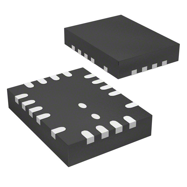
nn Small 18-Lead 3mm × 4mm QFN
The LT®8641 step-down regulator features Silent Switcher
architecture designed to minimize EMI emissions while
delivering high efficiency at frequencies up to 3MHz. Assembled in a 3mm × 4mm QFN, the monolithic construction with integrated power switches and inclusion of all
necessary circuitry yields a solution with a minimal PCB
footprint. An ultralow 2.5µA quiescent current—with the
output in full regulation—enables applications requiring
highest efficiency at very small load currents. Transient
response remains excellent and output voltage ripple is
below 10mVP-P at any load, from zero to full current.
nn
APPLICATIONS
Automotive and Industrial Supplies
General Purpose Step-Down
nn GSM Power Supplies
nn
nn
The LT8641 allows high VIN to low VOUT conversion at
high frequency with a fast minimum top switch on-time of
35ns. Operation is safe in overload even with a saturated
inductor.
Essential features are included and easy to use: An
open-drain PG pin signals when the output is in regulation. The SYNC/MODE pin selects between Burst Mode,
pulse-skipping, or spread spectrum mode, and also allows synchronization to an external clock. Soft-start and
tracking functionality is accessed via the TR/SS pin. An
accurate enable threshold can be set using the EN/UV pin
and a resistor at the RT pin programs switch frequency.
All registered trademarks and trademarks are the property of their respective owners. Protected
by U.S. patents, including 8823345.
TYPICAL APPLICATION
12VIN to 5VOUT Efficiency
5V 3.5A Step-Down Converter
4.7µF
1µF
EN/UV
GND1
PG
10nF
SYNC/MODE
TR/SS
BST
fSW = 1MHz
1µF
0.1µF 4.7µH
4.7pF
INTVCC
RT
VOUT
5V
3.5A
SW
BIAS
1µF
41.2k
95
2.275
90
VIN2
GND2
LT8641
2.600
1M
47µF
FB
GND
191k
85
1.625
80
1.300
0.975
75
70
POWER LOSS
65
60
0.5
8641 TA01a
1.950
EFFICIENCY
1
POWER LOSS (W)
VIN1
EFFICIENCY (%)
VIN
5.5V TO 65V
100
0.650
1MHz, L = 3.3μH
2MHz, L = 2.2μH 0.325
3MHz, L = 1.5μH
0
1.5
2
2.5
3
3.5
LOAD CURRENT (A)
8641 TA01b
Rev B
Document Feedback
For more information www.analog.com
1
�LT8641
PIN CONFIGURATION
VIN, EN/UV.................................................................65V
PG..............................................................................42V
BIAS...........................................................................25V
FB, TR/SS ...................................................................4V
SYNC/MODE Voltage ..................................................6V
Operating Junction Temperature Range (Note 2)
LT8641E.............................................. –40°C to 125°C
LT8641I............................................... –40°C to 125°C
LT8641H............................................. –40°C to 150°C
Storage Temperature Range................... –65°C to 150°C
SYNC/MODE
17
PG
20 19 18
FB
GND
TOP VIEW
16 TR/SS
BIAS 1
INTVCC 2
15 RT
BST 3
GND1 6
21
SW
14 EN/UV
13 VIN2
11 GND2
7
8
9
10
SW
22
SW
GND2
VIN1 4
SW
(Note 1)
GND1
ABSOLUTE MAXIMUM RATINGS
UDC PACKAGE
18-LEAD (3mm × 4mm) PLASTIC QFN
θJA = 40°C/W, θJC(PAD) = 12°C/W (NOTE 3)
EXPOSED PAD (PINS 21, 22) ARE SW, SHOULD BE SOLDERED TO PCB
NOTE: PINS 5 AND 12 ARE REMOVED. CONFIGURATION DOES NOT MATCH
JEDEC 20-LEAD PACKAGE OUTLINE
ORDER INFORMATION
LEAD FREE FINISH
TAPE AND REEL
PART MARKING*
PACKAGE DESCRIPTION
TEMPERATURE RANGE
LT8641EUDC#PBF
LT8641EUDC#TRPBF
LGSN
18-Lead (3mm × 4mm) Plastic QFN
–40°C to 125°C
LT8641IUDC#PBF
LT8641IUDC#TRPBF
LGSN
18-Lead (3mm × 4mm) Plastic QFN
–40°C to 125°C
LT8641HUDC#PBF
LT8641HUDC#TRPBF
LGSN
18-Lead (3mm × 4mm) Plastic QFN
–40°C to 150°C
Contact the factory for parts specified with wider operating temperature ranges. *The temperature grade is identified by a label on the shipping container.
Tape and reel specifications. Some packages are available in 500 unit reels through designated sales channels with #TRMPBF suffix.
ELECTRICAL
CHARACTERISTICS
The l denotes the specifications which apply over the full operating
temperature range, otherwise specifications are at TA = 25°C.
PARAMETER
CONDITIONS
MIN
Minimum Input Voltage
VIN Quiescent Current
TYP
MAX
l
2.6
3.0
V
l
0.75
0.75
3
10
µA
µA
l
1.7
1.7
4
10
µA
µA
0.3
0.5
mA
17
200
50
350
µA
µA
0.81
0.81
0.816
0.822
V
V
0.004
0.03
%/V
VEN/UV = 0V
VEN/UV = 2V, Not Switching, VSYNC = 0V
VEN/UV = 2V, Not Switching, VSYNC = 2V
VIN Current in Regulation
VOUT = 0.8V, VIN = 6V, Output Load = 100µA
VOUT = 0.8V, VIN = 6V, Output Load = 1mA
l
l
Feedback Reference Voltage
VIN = 6V, ILOAD = 0.5A
VIN = 6V, ILOAD = 0.5A
l
VIN = 4.0V to 42V, ILOAD = 0.5A
l
Feedback Voltage Line Regulation
2
0.804
0.79
UNITS
Rev B
For more information www.analog.com
�LT8641
ELECTRICAL
CHARACTERISTICS
The l denotes the specifications which apply over the full operating
temperature range, otherwise specifications are at TA = 25°C.
PARAMETER
CONDITIONS
MIN
Feedback Pin Input Current
VFB = 1V
–20
BIAS Pin Current Consumption
VBIAS = 3.3V, 2MHz
Minimum On-Time
ILOAD = 1.5A, SYNC = 0V
ILOAD = 1.5A, SYNC = 2V
RT = 221k
RT = 60.4k
RT = 18.2k
Top Power NMOS On-Resistance
ISW = 1A
MAX
20
9
l
l
Minimum Off-Time
Oscillator Frequency
TYP
l
l
l
180
665
1.85
l
Bottom Power NMOS On-Resistance
VINTVCC = 3.4V, ISW = 1A
Bottom Power NMOS Current Limit
VINTVCC = 3.4V
SW Leakage Current
VIN = 42V, VSW = 0V, 42V
mA
50
50
ns
ns
80
110
ns
210
700
2.00
240
735
2.15
kHz
kHz
MHz
EN/UV Pin Threshold
EN/UV Rising
6.2
8.2
4.8
5.8
mΩ
9.9
55
–15
l
0.95
EN/UV Pin Hysteresis
nA
35
35
105
Top Power NMOS Current Limit
UNITS
1.01
mΩ
7.25
A
15
µA
1.07
45
–20
A
V
mV
EN/UV Pin Current
VEN/UV = 2V
20
nA
PG Upper Threshold Offset from VFB
VFB Falling
l
5
7.5
10.25
%
PG Lower Threshold Offset from VFB
VFB Rising
l
–5.25
–8
–10.75
%
40
nA
750
2000
Ω
0.9
1.2
2.6
1.4
2.9
V
V
V
PG Hysteresis
0.4
PG Leakage
VPG = 3.3V
PG Pull-Down Resistance
VPG = 0.1V
SYNC/MODE Threshold
SYNC/MODE DC and Clock Low Level Voltage
SYNC/MODE Clock High Level Voltage
SYNC/MODE DC High Level Voltage
Spread Spectrum Modulation
Frequency Range
–40
l
0.7
2.3
RT = 60.4k, VSYNC = 3.3V
Spread Spectrum Modulation Frequency VSYNC = 3.3V
TR/SS Source Current
TR/SS Pull-Down Resistance
l
Fault Condition, TR/SS = 0.1V
Note 1: Stresses beyond those listed under Absolute Maximum Ratings
may cause permanent damage to the device. Exposure to any Absolute
Maximum Rating condition for extended periods may affect device
reliability and lifetime.
Note 2: The LT8641E is guaranteed to meet performance specifications
from 0°C to 125°C junction temperature. Specifications over the –40°C
to 125°C operating junction temperature range are assured by design,
characterization, and correlation with statistical process controls. The
LT8641I is guaranteed over the full –40°C to 125°C operating junction
temperature range. The LT8641H is guaranteed over the full –40°C to
150°C operating junction temperature range. High junction temperatures
degrade operating lifetimes. Operating lifetime is derated at junction
temperatures greater than 125°C.
1.2
%
22
%
2.5
kHz
1.9
220
2.6
µA
Ω
The junction temperature (TJ, in °C) is calculated from the ambient
temperature (TA in °C) and power dissipation (PD, in Watts) according to
the formula:
TJ = TA + (PD • θJA)
where θJA (in °C/W) is the package thermal impedance.
Note 3: θ values determined per JEDEC 51-7, 51-12. See Applications
Information section for information on improving the thermal resistance
and for actual temperature measurements of a demo board in typical
operating conditions.
Note 4: This IC includes overtemperature protection that is intended to
protect the device during overload conditions. Junction temperature will
exceed 150°C when overtemperature protection is active. Continuous
operation above the specified maximum operating junction temperature
will reduce lifetime.
Rev B
For more information www.analog.com
3
�LT8641
TYPICAL PERFORMANCE CHARACTERISTICS
12VIN to 5VOUT Efficiency
vs Frequency
12VIN to 3.3VOUT Efficiency
vs Frequency
2.3
95
1.9
80
1.3
1.0
75
POWER LOSS
65
60
0.5
1
L = WE–LHMI7050 0.7
1MHz, L = 3.3μH
2MHz, L = 2.2μH 0.3
3MHz, L = 1.5μH
0
1.5
2
2.5
3
3.5
LOAD CURRENT (A)
1.2
80
0.9
75
POWER LOSS
70
L = WE–LHMI7050 0.6
1MHz, L = 2.2µH
2MHz, L = 1.5µH 0.3
3MHz, L = 1µH
0
1.5
2
2.5
3
3.5
LOAD CURRENT (A)
65
60
0.5
1
8641 G01
Efficiency at 3.3V OUT
EFFICIENCY
fSW = 1MHz
L = WE–LHMI7050, 2.2µH 2.3
90
2.0
85
1.8
80
1.5
75
1.3
70
1.0
65
0.8
60
55
50
POWER LOSS
0
0.5
100
2.5
1
1.5
2
2.5
LOAD CURRENT (A)
POWER LOSS (W)
EFFICIENCY (%)
95
2.0
85
1.8
80
1.5
fSW = 1MHz
75 L = WE–LHMI7050, 4.7µH
1.0
65
0.8
VIN = 12V
VIN = 24V 0.5
VIN = 36V 0.3
VIN = 48V
POWER LOSS
0
0.5
1
1.5
2
2.5
3
3.5
LOAD CURRENT (A)
60
55
50
0
8641 G03
Efficiency at 5V OUT
100
90
90
80
80
70
60
50
VIN = 12V
0.5
VIN = 24V
VIN = 36V 0.3
VIN = 48V
0
3
3.5
40
fSW = 1MHz
L = WE–LHMI7050, 4.7µH
30
20
0.01
0.1
8641 G04
VIN = 12V
VIN = 24V
VIN = 36V
VIN = 48V
1
10
100
LOAD CURRENT (mA)
Efficiency at 3.3V OUT
70
60
50
40
30
20
0.01
1000
fSW = 1MHz
L = WE–LHMI7050, 4.7µH
0.1
1
10
100
LOAD CURRENT (mA)
8641 G05
96
88
VIN = 24V
86
82
80
0.5
VIN = 24V
85
80
75
VOUT = 3.3V
ILOAD = 1.5A
L = WE–LHMI7050, 4.7µH
1.0
1.5
2.0
2.5
SWITCHING FREQUENCY (MHz)
VOUT = 5V
ILOAD = 10mA
L = WE–LHMI7050
70
3.0
8641 G07
4
817
65
1
2
3
4
5
6
7
8
INDUCTOR VALUE (µH)
9
10
8641 G08
REFERENCE VOLTAGE (mV)
90
84
VIN = 12V
90
EFFICIENCY (%)
EFFICIENCY (%)
92
819
95
VIN = 12V
1000
Reference
Reference Voltage
Voltage
100
94
VIN = 12V
V = 24V
VIN = 36V
VIN = 48V
8641 G06
Burst Mode Operation Efficiency
vs Inductor Value
Efficiency vs Frequency
1.3
70
8641 G02
EFFICIENCY (%)
100
1.5
2.3
90
EFFICIENCY (%)
70
EFFICIENCY
85
2.5
EFFICIENCY
POWER LOSS (W)
1.6
1.8
POWER LOSS (W)
85
90
EFFICIENCY (%)
EFFICIENCY
Efficiency at 5V OUT
95
2.1
95
POWER LOSS (W)
EFFICIENCY (%)
90
100
2.4
100
EFFICIENCY (%)
2.6
100
815
813
811
809
807
805
803
801
–50 –25
0
25 50 75 100 125 150
TEMPERATURE (°C)
8641 G09
Rev B
For more information www.analog.com
�LT8641
TYPICAL PERFORMANCE CHARACTERISTICS
EN
EN Pin
Pin Thresholds
Thresholds
1.02
0.99
0.98
EN FALLING
0
0.05
0
–0.05
0
0.5
1
1.5
2
2.5
LOAD CURRENT (A)
3
–0.15
2.0
15
25
35
45
INPUT VOLTAGE (V)
55
65
8641 G12
Top
Top FET
FET Current
Current Limit
Limit
10
9
CURRENT LIMIT (A)
2.5
5
8.0
CURRENT LIMIT (A)
7.5
7.0
6.5
8
5% DC
7
6.0
0
10
20
30
40
50
INPUT VOLTAGE (V)
60
5.5
0.1
0.3
0.5
DUTY CYCLE
0.7
6
–50 –25
0.9
8641 G14
8641 G13
Switch Drop
500
SWITCH CURRENT = 1A
43
40
400
SWITCH DROP (mV)
150
TOP SWITCH
100
50
350
300
250
TOP SWITCH
200
150
100
BOTTOM SWITCH
0
25 50 75 100 125 150
TEMPERATURE (°C)
0
0
0.5
1
1.5
2
2.5
SWITCH CURRENT (A)
3
3.5
8641 G17
8641 G16
37
34
31
28
BOTTOM SWITCH
50
0
–50 –25
VSYNC = 0
VSYNC = FLOAT
450
200
25 50 75 100 125 150
TEMPERATURE (°C)
Minimum On-Time
Switch Drop
250
0
8641 G15
MINIMUM ON-TIME (ns)
INPUT CURRENT (µA)
3.0
1.5
SWITCH DROP (mV)
3.5
8.5
VOUT = 3.3V
L = 4.7µH
IN-REGULATION
3.5
1.0
–0.05
Top FET Current Limit vs Duty Cycle
No-Load Supply Current
4.0
0
8641 G11
8641 G10
4.5
0.05
–0.10
–0.15
25 50 75 100 125 150
TEMPERATURE (°C)
VOUT = 5V
ILOAD = 1A
0.10
–0.10
0.96
0.95
–50 –25
VOUT = 5V
VIN = 12V
CHANGE IN VOUT (%)
CHANGE IN VOUT (%)
EN THRESHOLD (V)
1.00
0.97
0.15
0.10
EN RISING
1.01
Line Regulation
Load Regulation
0.15
1.03
25
–50
ILOAD = 2A
–25
0
25
50
75
TEMPERATURE (°C)
100
125
8641 G18
Rev B
For more information www.analog.com
5
�LT8641
TYPICAL PERFORMANCE CHARACTERISTICS
Dropout Voltage
VIN = 5V
VOUT SET TO REGULATE AT 5V
L = WE–LHMI7050, 1µH
400
300
200
100
0
720
710
700
690
680
0
0.5
1
1.5
2
2.5
LOAD CURRENT (A)
3
660
–50 –25
3.5
0
400
200
0
25 50 75 100 125 150
TEMPERATURE (°C)
60
40
20
200
400
600
LOAD CURRENT (mA)
600
800
Soft-Start Tracking
1.0
0.8
FB VOLTAGE (V)
SWITCHING FREQUENCY (kHz)
80
0
8641 G21
VOUT = 3.3V
VIN = 12V
VSYNC = 0V
RT = 60.4k
700
100
0
600
Frequency Foldback
800
FRONT PAGE APPLICATION
VOUT = 5V
fSW = 1MHz
120
800
8641 G20
Minimum Load to Full Frequency
(Pulse-Skipping Mode)
140
FRONT PAGE APPLICATION
VIN = 12V
VOUT = 5V
1000
670
8641 G19
LOAD CURRENT (mA)
Burst Frequency
1200
RT = 60.4k
730
SWITCHING FREQUENCY (kHz)
500
DROPOUT VOLTAGE (mV)
Switching
SwitchingFrequency
Frequency
740
SWITCHING FREQUENCY (kHz)
600
500
400
300
200
0.6
0.4
0.2
100
5
15
25
35
45
INPUT VOLTAGE (V)
55
0
65
0
0.2
8641 G22
0.4
0.6
FB VOLTAGE (V)
0.8
0
1
0
0.2
0.4
0.6
0.8
TR/SS VOLTAGE (V)
1.0
1.2
8641 G24
8641 G23
Soft-StartCurrent
Current
Soft–Start
VSS = 0.5V
2.0
1.9
1.8
1.7
1.6
1.5
1.4
–50 –25
0
–6.0
25 50 75 100 125 150
TEMPERATURE (°C)
9.5
9.0
8.5
FB RISING
8.0
7.5
FB FALLING
7.0
6.5
6.0
–50 –25
0
25 50 75 100 125 150
TEMPERATURE (°C)
8641 G25
6
PG THRESHOLD OFFSET FROM VREF (%)
SS PIN CURRENT (µA)
2.1
PG
PG Low
Low Thresholds
Thresholds
PG High Thresholds
10.0
PG THRESHOLD OFFSET FROM VREF (%)
2.2
8641 G26
–6.5
–7.0
–7.5
FB RISING
–8.0
–8.5
FB FALLING
–9.0
–9.5
–10.0
–50 –25
0
25 50 75 100 125 150
TEMPERATURE (°C)
8641 G27
Rev B
For more information www.analog.com
�LT8641
TYPICAL PERFORMANCE CHARACTERISTICS
RT Programmed Switching
Frequency
VMinimum
IN UVLO Input Voltage
250
Bias Pin Current
3.2
7.5
3.0
7.0
VBIAS = 5V
VOUT = 5V
ILOAD = 1A
fSW = 1MHz
175
INPUT VOLTAGE (V)
RT PIN RESISTOR (kΩ)
200
150
125
100
75
50
BIAS PIN CURRENT (mA)
225
2.8
2.6
2.4
0
0.2
0.6
1.4 1.8 2.2 2.6
1
SWITCHING FREQUENCY (MHz)
2.0
–50 –25
3
6.0
5.5
5.0
2.2
25
6.5
0
4.5
25 50 75 100 125 150
TEMPERATURE (°C)
5
15
25
35
45
INPUT VOLTAGE (V)
55
65
8641 G30
8641 G29
8641 G28
10
5
0
0.2
0.6 1.0 1.4 1.8 2.2 2.6
SWITCHING FREQUENCY (MHz)
3.0
50
40
20
10
0
500ns/DIV
FRONT PAGE APPLICATION
12VIN TO 5VOUT AT 1A
8641 G34
70
60
50
40
30
20
10
0
0.5
1
1.5
2
2.5
LOAD CURRENT (A)
3
3.5
0
0
0.2
0.4
0.6
DUTY CYCLE OF 5A LOAD
Switching Waveforms, Burst
Mode Operation
Switching Waveforms
IL
500mA/DIV
IL
1A/DIV
VSW
5V/DIV
VSW
20V/DIV
10µs/DIV
FRONT PAGE APPLICATION
12VIN TO 5VOUT AT 10mA
VSYNC = 0V
0.8
8641 G33
8641 G32
Switching Waveforms, Full
Frequency Continuous Operation
VSW
5V/DIV
DC2373A DEMO BOARD
VIN = 12V
VOUT = 5V
fSW = 2MHz
STANDBY LOAD = 0.25A
1kHz PULSED LOAD = 5A
80
30
8641 G31
IL
1A/DIV
DC2373A DEMO BOARD
VIN = 12V, fSW = 1MHz
VIN = 24V, fSW = 1MHz
VIN = 12V, fSW = 2MHz
VIN = 24V, fSW = 2MHz
CASE TEMPERATURE RISE (°C)
15
90
60
VBIAS = 5V
VOUT = 5V
VIN = 12V
ILOAD = 1A
CASE TEMPERATURE RISE (°C)
BIAS PIN CURRENT (mA)
20
Case Temperature Rise vs 5A
Pulsed Load
Case
Case Temperature
Temperature Rise
Rise
Bias Pin Current
8641 G35
500ns/DIV
FRONT PAGE APPLICATION
48VIN TO 5VOUT AT 1A
8641 G36
Rev B
For more information www.analog.com
7
�LT8641
TYPICAL PERFORMANCE CHARACTERISTICS
Transient Response; Load Current
Stepped from 300mA (Burst Mode
Operation) to 1.3A
Transient Response; Load Current
Stepped from 1A to 2A
ILOAD
1A/DIV
ILOAD
1A/DIV
VOUT
100mA/DIV
VOUT
200mA/DIV
8641 G37
50µs/DIV
50µs/DIV
FRONT PAGE APPLICATION
300mA (Burst Mode OPERATION) TO
1.3A TRANSIENT
12VIN, 5VOUT
COUT = 47µF
FRONT PAGE APPLICATION
1A TO 2A TRANSIENT
12VIN, 5VOUT
COUT = 47µF
Start-Up Dropout Performance
Start-Up Dropout Performance
VIN
VIN
2V/DIV
VIN
VIN
2V/DIV
VOUT
VOUT
2V/DIV
8641 G38
VOUT
VOUT
2V/DIV
100ms/DIV
2.5Ω LOAD
(2A IN REGULATION)
100ms/DIV
20Ω LOAD
(250mA IN REGULATION)
8641 G39
8641 G40
Conducted EMI Performance
60
50
AMPLITUDE (dBµV)
40
30
20
10
0
–10
–20
SPREAD SPECTRUM MODE
FIXED FREQUENCY MODE
–30
–40
0
3
6
9
12
15
18
21
FREQUENCY (MHz)
24
27
30
8641 G41
DC2373A DEMO BOARD
(WITH EMI FILTER INSTALLED)
14V INPUT TO 5V OUTPUT AT 3.5A, fSW = 2MHz
8
Rev B
For more information www.analog.com
�LT8641
TYPICAL PERFORMANCE CHARACTERISTICS
Radiated EMI Performance
(CISPR25 Radiated Emission Test with Class 5 Peak Limits)
50
VERTICAL POLARIZATION
PEAK DETECTOR
45
AMPLITUDE (dBµV/m)
40
35
30
25
20
15
10
5
CLASS 5 PEAK LIMIT
FIXED FREQUENCY MODE
SPREAD SPECTRUM MODE
0
–5
0
100
200
300
400
500
600
700
800
900
1000
FREQUENCY (MHz)
50
HORIZONTAL POLARIZATION
PEAK DETECTOR
45
AMPLITUDE (dBµV/m)
40
35
30
25
20
15
10
5
CLASS 5 PEAK LIMIT
FIXED FREQUENCY MODE
SPREAD SPECTRUM MODE
0
-5
0
100
200
300
400
500
600
700
800
900
1000
FREQUENCY (MHz)
DC2373A DEMO BOARD
(WITH EMI FILTER INSTALLED)
14V INPUT TO 5V OUTPUT AT 3.5A, fSW = 2MHz
8641 G42
Rev B
For more information www.analog.com
9
�LT8641
PIN FUNCTIONS
BIAS (Pin 1): The internal regulator will draw current
from BIAS instead of VIN when BIAS is tied to a voltage
higher than 3.1V. For output voltages of 3.3V to 25V this
pin should be tied to VOUT. If this pin is tied to a supply
other than VOUT use a 1µF local bypass capacitor on this
pin. If no supply is available, tie to GND.
GND2 (10, 11): Power Switch Ground. These pins are the
return path of the internal bottom side power switch and
must be tied together. Place the negative terminal of the
input capacitor as close to the GND2 pins as possible. Also
be sure to tie GND2 to the ground plane. See the Applications Information section for sample layout.
INTVCC (Pin 2): Internal 3.4V Regulator Bypass Pin. The
internal power drivers and control circuits are powered from
this voltage. INTVCC maximum output current is 20mA.
Do not load the INTVCC pin with external circuitry. INTVCC
current will be supplied from BIAS if BIAS > 3.1V, otherwise
current will be drawn from VIN. Voltage on INTVCC will
vary between 2.8V and 3.4V when BIAS is between 3.0V
and 3.6V. Decouple this pin to power ground with at least
a 1μF low ESR ceramic capacitor placed close to the IC.
VIN2 (Pin 13): The LT8641 requires two 1µF small input
bypass capacitors. One 1µF capacitor should be placed
between VIN1 and GND1. A second 1µF capacitor should
be placed between VIN2 and GND2. These capacitors must
be placed as close as possible to the LT8641. A third larger
capacitor of 2.2µF or more should be placed close to the
LT8641 with the positive terminal connected to VIN1 and
VIN2, and the negative terminal connected to ground. See
the Applications Information section for sample layout.
BST (Pin 3): This pin is used to provide a drive voltage,
higher than the input voltage, to the topside power switch.
Place a 0.1µF boost capacitor as close as possible to the IC.
EN/UV (Pin 14): The LT8641 is shut down when this pin
is low and active when this pin is high. The hysteretic
threshold voltage is 1.00V going up and 0.96V going
down. Tie to VIN if the shutdown feature is not used. An
external resistor divider from VIN can be used to program
a VIN threshold below which the LT8641 will shut down.
VIN1 (Pin 4): The LT8641 requires two 1µF small input
bypass capacitors. One 1µF capacitor should be placed
between VIN1 and GND1. A second 1µF capacitor should
be placed between VIN2 and GND2. These capacitors must
be placed as close as possible to the LT8641. A third larger
capacitor of 2.2µF or more should be placed close to the
LT8641 with the positive terminal connected to VIN1 and
VIN2, and the negative terminal connected to ground. See
applications section for sample layout.
GND1 (6, 7): Power Switch Ground. These pins are the
return path of the internal bottom side power switch and
must be tied together. Place the negative terminal of the
input capacitor as close to the GND1 pins as possible. Also
be sure to tie GND1 to the ground plane. See the Applications Information section for sample layout.
SW (Pins 8, 9): The SW pins are the outputs of the internal
power switches. Tie these pins together and connect them
to the inductor and boost capacitor. This node should be
kept small on the PCB for good performance and low EMI.
10
RT (Pin 15): A resistor is tied between RT and ground to
set the switching frequency.
TR/SS (Pin 16): Output Tracking and Soft-Start Pin. This
pin allows user control of output voltage ramp rate during
start-up. A TR/SS voltage below 0.8V forces the LT8641 to
regulate the FB pin to equal the TR/SS pin voltage. When
TR/SS is above 0.8V, the tracking function is disabled
and the internal reference resumes control of the error
amplifier. An internal 1.9μA pull-up current from INTVCC
on this pin allows a capacitor to program output voltage
slew rate. This pin is pulled to ground with an internal 200Ω
MOSFET during shutdown and fault conditions; use a series
resistor if driving from a low impedance output. This pin
may be left floating if the tracking function is not needed.
Rev B
For more information www.analog.com
�LT8641
PIN FUNCTIONS
SYNC/MODE (Pin 17): This pin programs four different
operating modes: 1) Burst Mode. Tie this pin to ground
for Burst Mode operation at low output loads—this will
result in ultralow quiescent current. 2) Pulse-skipping
mode. Float this pin for pulse-skipping mode. This mode
offers full frequency operation down to low output loads
before pulse skipping occurs. When floating, pin leakage
currents should be 0.5), a
minimum inductance is required to avoid subharmonic
oscillation (See Equation 10). See Application Note 19
for more details.
V •(2 •DC – 1)
L MIN = IN
2.5 • fSW
(10)
where DC is the duty cycle ratio (VOUT/VIN) and fSW is the
switching frequency.
Input Capacitors
The VIN of the LT8641 should be bypassed with at least
three ceramic capacitors for best performance. Two small
ceramic capacitors of 1µF should be placed close to the
part; one at the VIN1/GND1 pins and a second at VIN2/GND2
pins. These capacitors should be 0402 or 0603 in size. For
automotive applications requiring 2 series input capacitors, two small 0402 or 0603 may be placed at each side
of the LT8641 near the VIN1/GND1 and VIN2/GND2 pins.
A third, larger ceramic capacitor of 2.2µF or larger should
be placed close to VIN1 or VIN2. See Low EMI PCB Layout
section for more detail. X7R or X5R capacitors are recommended for best performance across temperature and
input voltage variations.
Note that larger input capacitance is required when a lower
switching frequency is used. If the input power source has
Rev B
For more information www.analog.com
17
�LT8641
APPLICATIONS INFORMATION
high impedance, or there is significant inductance due to
long wires or cables, additional bulk capacitance may be
necessary. This can be provided with a low performance
electrolytic capacitor.
A ceramic input capacitor combined with trace or cable
inductance forms a high quality (under damped) tank circuit. If the LT8641 circuit is plugged into a live supply, the
input voltage can ring to twice its nominal value, possibly
exceeding the LT8641’s voltage rating. This situation is
easily avoided (see Linear Technology Application Note 88).
Output Capacitor and Output Ripple
The output capacitor has two essential functions. Along
with the inductor, it filters the square wave generated
by the LT8641 to produce the DC output. In this role it
determines the output ripple, thus low impedance at the
switching frequency is important. The second function
is to store energy in order to satisfy transient loads and
stabilize the LT8641’s control loop. Ceramic capacitors
have very low equivalent series resistance (ESR) and
provide the best ripple performance. For good starting
values, see the Typical Applications section.
Use X5R or X7R types. This choice will provide low output
ripple and good transient response. Transient performance
can be improved with a higher value output capacitor and
the addition of a feedforward capacitor placed between
VOUT and FB. Increasing the output capacitance will also
decrease the output voltage ripple. A lower value of output
capacitor can be used to save space and cost but transient
performance will suffer and may cause loop instability. See
the Typical Applications in this data sheet for suggested
capacitor values.
When choosing a capacitor, special attention should be
given to the data sheet to calculate the effective capacitance
under the relevant operating conditions of voltage bias and
temperature. A physically larger capacitor or one with a
higher voltage rating may be required.
18
Ceramic Capacitors
Ceramic capacitors are small, robust and have very low
ESR. However, ceramic capacitors can cause problems
when used with the LT8641 due to their piezoelectric nature.
When in Burst Mode operation, the LT8641’s switching
frequency depends on the load current, and at very light
loads the LT8641 can excite the ceramic capacitor at audio
frequencies, generating audible noise. Since the LT8641
operates at a lower current limit during Burst Mode operation, the noise is typically very quiet to a casual ear. If
this is unacceptable, use a high performance tantalum or
electrolytic capacitor at the output. Low noise ceramic
capacitors are also available.
A final precaution regarding ceramic capacitors concerns
the maximum input voltage rating of the LT8641. As
previously mentioned, a ceramic input capacitor combined
with trace or cable inductance forms a high quality (underdamped) tank circuit. If the LT8641 circuit is plugged
into a live supply, the input voltage can ring to twice its
nominal value, possibly exceeding the LT8641’s rating.
This situation is easily avoided (see Linear Technology
Application Note 88).
Enable Pin
The LT8641 is in shutdown when the EN pin is low and
active when the pin is high. The rising threshold of the EN
comparator is 1.01V, with 45mV of hysteresis. The EN pin
can be tied to VIN if the shutdown feature is not used, or
tied to a logic level if shutdown control is required.
Adding a resistor divider from VIN to EN programs the
LT8641 to regulate the output only when VIN is above a
desired voltage (see the Block Diagram). Typically, this
threshold, VIN(EN), is used in situations where the input
supply is current limited, or has a relatively high source
resistance. A switching regulator draws constant power
from the source, so source current increases as source
voltage drops. This looks like a negative resistance load
Rev B
For more information www.analog.com
�LT8641
APPLICATIONS INFORMATION
to the source and can cause the source to current limit or
latch low under low source voltage conditions. The VIN(EN)
threshold prevents the regulator from operating at source
voltages where the problems might occur. This threshold
can be adjusted by setting the values R3 and R4 such that
they satisfy the following equation:
⎛ R3 ⎞
VIN(EN ) = ⎜
+ 1⎟ • 1.01V
⎝ R4 ⎠
(11)
where the LT8641 will remain off until VIN is above VIN(EN).
Due to the comparator’s hysteresis, switching will not stop
until the input falls slightly below VIN(EN).
When operating in Burst Mode operation for light load
currents, the current through the VIN(EN) resistor network
can easily be greater than the supply current consumed
by the LT8641. Therefore, the VIN(EN) resistors should be
large to minimize their effect on efficiency at low loads.
INTVCC Regulator
An internal low dropout (LDO) regulator produces the 3.4V
supply from VIN that powers the drivers and the internal
bias circuitry. The INTVCC can supply enough current for
the LT8641’s circuitry and must be bypassed to ground
with a minimum of 1μF ceramic capacitor. Good bypassing
is necessary to supply the high transient currents required
by the power MOSFET gate drivers. To improve efficiency
the internal LDO can also draw current from the BIAS
pin when the BIAS pin is at 3.1V or higher. Typically the
BIAS pin can be tied to the output of the LT8641, or can
be tied to an external supply of 3.3V or above. If BIAS is
connected to a supply other than VOUT, be sure to bypass
with a local ceramic capacitor. If the BIAS pin is below
3.0V, the internal LDO will consume current from VIN.
Applications with high input voltage and high switching
frequency where the internal LDO pulls current from VIN
will increase die temperature because of the higher power
dissipation across the LDO. Do not connect an external
load to the INTVCC pin.
Output Voltage Tracking and Soft-Start
The LT8641 allows the user to program its output voltage
ramp rate by means of the TR/SS pin. An internal 1.9μA
pulls up the TR/SS pin to INTVCC. Putting an external
capacitor on TR/SS enables soft starting the output to prevent current surge on the input supply. During the soft-start
ramp the output voltage will proportionally track the TR/SS
pin voltage. For output tracking applications, TR/SS can
be externally driven by another voltage source. From 0V
to 0.8V, the TR/SS voltage will override the internal 0.8V
reference input to the error amplifier, thus regulating the
FB pin voltage to that of TR/SS pin. When TR/SS is above
0.8V, tracking is disabled and the feedback voltage will
regulate to the internal reference voltage. The TR/SS pin
may be left floating if the function is not needed.
An active pull-down circuit is connected to the TR/SS pin
which will discharge the external soft-start capacitor in
the case of fault conditions and restart the ramp when the
faults are cleared. Fault conditions that clear the soft-start
capacitor are the EN/UV pin transitioning low, VIN voltage
falling too low, or thermal shutdown.
Output Power Good
When the LT8641’s output voltage is within the ±8%
window of the regulation point, the output voltage is
considered good and the open-drain PG pin goes high
impedance and is typically pulled high with an external
resistor. Otherwise, the internal pull-down device will pull
the PG pin low. To prevent glitching both the upper and
lower thresholds include 0.4% of hysteresis.
The PG pin is also actively pulled low during several fault
conditions: EN/UV pin is below 1V, INTVCC has fallen too
low, VIN is too low, or thermal shutdown.
Synchronization and Spread Spectrum
To select low ripple Burst Mode operation, tie the SYNC pin
below 0.4V (this can be ground or a logic low output). To
synchronize the LT8641 oscillator to an external frequency
connect a square wave (with 20% to 80% duty cycle) to
the SYNC pin. The square wave amplitude should have valleys that are below 0.4V and peaks above 1.5V (up to 6V).
Rev B
For more information www.analog.com
19
�LT8641
APPLICATIONS INFORMATION
The LT8641 will not enter Burst Mode operation at low
output loads while synchronized to an external clock, but
instead will pulse skip to maintain regulation. The LT8641
may be synchronized over a 200kHz to 3MHz range. The
RT resistor should be chosen to set the LT8641 switching
frequency equal to or below the lowest synchronization
input. For example, if the synchronization signal will be
500kHz and higher, the RT should be selected for 500kHz.
The slope compensation is set by the RT value, while the
minimum slope compensation required to avoid subharmonic oscillations is established by the inductor size,
input voltage, and output voltage. Since the synchronization frequency will not change the slopes of the inductor
current waveform, if the inductor is large enough to avoid
subharmonic oscillations at the frequency set by RT, then
the slope compensation will be sufficient for all synchronization frequencies.
For some applications it is desirable for the LT8641 to
operate in pulse-skipping mode, offering two major differences from Burst Mode operation. First is the clock stays
awake at all times and all switching cycles are aligned
to the clock. Second is that full switching frequency is
reached at lower output load than in Burst Mode operation.
These two differences come at the expense of increased
quiescent current. To enable pulse-skipping mode, the
SYNC pin is floated. Leakage current on this pin should
be 3.1V
OR GND
VOUT
1.8V
3.5A
10pF
1M
825k
GND
fSW = 2MHz
L: VISHAY IHLP2525CZ-01
100µF
1210
X5R/X7R
8641 TA07
RELATED PARTS
PART
DESCRIPTION
COMMENTS
LT8640/
LT8640-1
42V, 5A, 96% Efficiency, 3MHz Synchronous MicroPower Step-Down
DC/DC Converter with IQ = 2.5µA
VIN(MIN) = 3.4V, VIN(MAX) = 42V, VOUT(MIN) = 0.97V, IQ = 2.5μA,
ISD < 1μA, 3mm × 4mm QFN-18
LT8609/
LT8609A
42V, 2A, 94% Efficiency, 2.2MHz Synchronous MicroPower Step-Down
DC/DC Converter with IQ = 2.5µA
VIN(MIN) = 3V, VIN(MAX) = 42V, VOUT(MIN) = 0.8V, IQ = 2.5μA,
ISD < 1μA, MSOP-10E
LT8610A/
LT8610AB
42V, 3.5A, 96% Efficiency, 2.2MHz Synchronous MicroPower Step-Down
DC/DC Converter with IQ = 2.5µA
VIN(MIN) = 3.4V, VIN(MAX) = 42V, VOUT(MIN) = 0.97V, IQ = 2.5μA,
ISD < 1μA, MSOP-16E
LT8610AC
42V, 3.5A, 96% Efficiency, 2.2MHz Synchronous MicroPower Step-Down
DC/DC Converter with IQ = 2.5µA
VIN(MIN) = 3V, VIN(MAX) = 42V, VOUT(MIN) = 0.8V, IQ = 2.5μA,
ISD < 1μA, MSOP-16E
LT8610
42V, 2.5A, 96% Efficiency, 2.2MHz Synchronous MicroPower Step-Down
DC/DC Converter with IQ = 2.5µA
VIN(MIN) = 3.4V, VIN(MAX) = 42V, VOUT(MIN) = 0.97V, IQ = 2.5μA,
ISD < 1μA, MSOP-16E
LT8611
42V, 2.5A, 96% Efficiency, 2.2MHz Synchronous MicroPower Step-Down
DC/DC Converter with IQ = 2.5µA and Input/Output Current
Limit/Monitor
VIN(MIN) = 3.4V, VIN(MAX) = 42V, VOUT(MIN) = 0.97V, IQ = 2.5μA,
ISD < 1μA, 3mm × 5mm QFN-24
LT8616
42V, Dual 2.5A + 1.5A, 95% Efficiency, 2.2MHz Synchronous MicroPower VIN(MIN) = 3.4V, VIN(MAX) = 42V, VOUT(MIN) = 0.8V, IQ = 5μA,
Step-Down DC/DC Converter with IQ = 5µA
ISD < 1μA, TSSOP-28E, 3mm × 6mm QFN-28
LT8620
65V, 2.5A, 94% Efficiency, 2.2MHz Synchronous MicroPower Step-Down
DC/DC Converter with IQ = 2.5µA
LT8614
42V, 4A, 96% Efficiency, 2.2MHz Synchronous Silent Switcher Step-Down VIN(MIN) = 3.4V, VIN(MAX) = 42V, VOUT(MIN) = 0.97V, IQ = 2.5μA,
DC/DC Converter with IQ = 2.5µA
ISD < 1μA, 3mm × 4mm QFN18
LT8612
42V, 6A, 96% Efficiency, 2.2MHz Synchronous MicroPower Step-Down
DC/DC Converter with IQ = 2.5µA
VIN(MIN) = 3.4V, VIN(MAX) = 42V, VOUT(MIN) = 0.97V, IQ = 3.0μA,
ISD < 1μA, 3mm × 6mm QFN-28
LT8613
42V, 6A, 96% Efficiency, 2.2MHz Synchronous MicroPower Step-Down
DC/DC Converter with Current Limiting
VIN(MIN) = 3.4V, VIN(MAX) = 42V, VOUT(MIN) = 0.97V, IQ = 3.0μA,
ISD < 1μA, 3mm × 6mm QFN-28
LT8602
42V, Quad Output (2.5A + 1.5A + 1.5A + 1.5A) 95% Efficiency, 2.2MHz
Synchronous MicroPower Step-Down DC/DC Converter with IQ = 25µA
VIN(MIN) = 3V, VIN(MAX) = 42V, VOUT(MIN) = 0.8V, IQ = 2.5μA,
ISD < 1μA, 6mm × 6mm QFN-40
26
VIN(MIN) = 3.4V, VIN(MAX) = 65V, VOUT(MIN) = 0.97V, IQ = 2.5μA,
ISD < 1μA, MSOP-16E, 3mm × 5mm QFN-24
Rev B
D16866-0-8/18(B)
For more information www.analog.com
www.analog.com
© ANALOG DEVICES, INC. 2016-2018
�


 工商网监
湘ICP备2023018690号
工商网监
湘ICP备2023018690号

