LTC1050
Precision Zero-Drift
Operational Amplifier
with Internal Capacitors
DESCRIPTIO
U
FEATURES
■
■
■
■
■
■
■
■
■
■
■
■
■
■
No External Components Required
Noise Tested and Guaranteed
Low Aliasing Errors
Maximum Offset Voltage: 5µV
Maximum Offset Voltage Drift: 0.05µV/°C
Low Noise: 1.6µVP-P (0.1Hz to 10Hz)
Minimum Voltage Gain: 130dB
Minimum PSRR: 125dB
Minimum CMRR: 120dB
Low Supply Current: 1mA
Single Supply Operation: 4.75V to 16V
Input Common Mode Range Includes Ground
Output Swings to Ground
Typical Overload Recovery Time: 3ms
U
APPLICATIO S
■
■
■
■
■
■
The LTC®1050 is a high performance, low cost zero-drift
operational amplifier. The unique achievement of the
LTC1050 is that it integrates on-chip the two sample-andhold capacitors usually required externally by other chopper amplifiers. Further, the LTC1050 offers better combined overall DC and AC performance than is available
from other chopper stabilized amplifiers with or without
internal sample-and-hold capacitors.
The LTC1050 has an offset voltage of 0.5µV, drift of
0.01µV/°C, DC to 10Hz, input noise voltage of 1.6µVP-P
and a typical voltage gain of 160dB. The slew rate of 4V/µs
and a gain bandwidth product of 2.5MHz are achieved with
only 1mA of supply current.
Overload recovery times from positive and negative saturation conditions are 1.5ms and 3ms respectively, which
represents an improvement of about 100 times over chopper amplifiers using external capacitors. Pin 5 is an optional
external clock input, useful for synchronization purposes.
Thermocouple Amplifiers
Electronic Scales
Medical Instrumentation
Strain Gauge Amplifiers
High Resolution Data Acquisition
DC Accurate RC Active Filters
The LTC1050 is available in standard 8-pin metal can,
plastic and ceramic dual-in-line packages as well as an
SO-8 package. The LTC1050 can be an improved plug-in
replacement for most standard op amps.
, LTC and LT are registered trademarks of Linear Technology Corporation.
U
TYPICAL APPLICATIO
High Performance, Low Cost Instrumentation Amplifier
Noise Spectrum
5V
4
5V
1/2 LTC1043
7
3
8
+
7
LTC1050
2
11
DIFFERENTIAL
INPUT
CH
1µF
CS
1µF
–
6
VOUT
4
– 5V
1µF
12
R1
13
R2
1050 TA01
17
0.01µF
– 5V
140
120
100
80
60
40
20
0
14
16
VOLTAGE NOISE DENSITY (nV/√Hz)
160
CMRR > 120dB AT DC
CMRR > 120dB AT 60Hz
DUAL SUPPLY OR SINGLE 5V
GAIN = 1 + R2/R1
VOS = 5µV
COMMON MODE INPUT VOLTAGE EQUALS THE SUPPLIES
10
100
1k
10k
FREQUENCY (Hz)
100k
1050 TA02
1050fb
1
�LTC1050
W W
W
AXI U
U
ABSOLUTE
RATI GS (Note 1)
Total Supply Voltage (V + to V –) .............................. 18V
Input Voltage ........................ (V + + 0.3V) to (V – – 0.3V)
Output Short-Circuit Duration ......................... Indefinite
Storage Temperature Range ................ – 65°C to 150°C
Lead Temperature (Soldering, 10 sec)................. 300°C
Operating Temperature Range
LTC1050AC/C .................................. – 40°C to 85°C
LTC1050H ..................................... – 40°C to 125°C
LTC1050AM/M (OBSOLETE) .......... – 55°C to 125°C
U
W
U
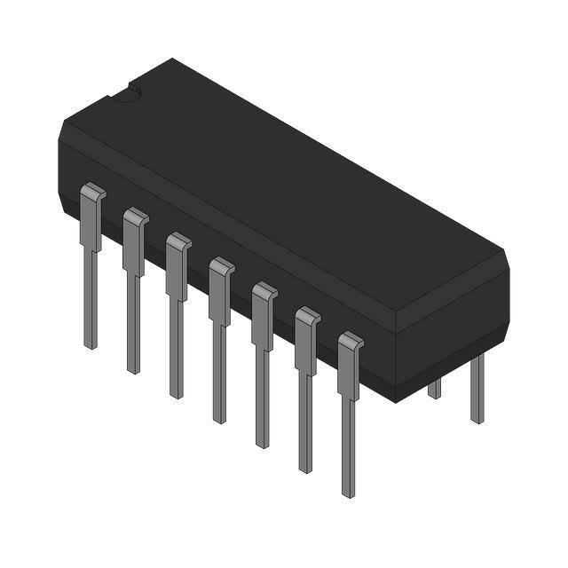
PACKAGE/ORDER I FOR ATIO
ORDER PART
NUMBER
TOP VIEW
NC
8
NC 1
7 V + (CASE)
–IN 2
6 OUT
+IN 3
4
5 EXT CLOCK
INPUT
ORDER PART
NUMBER
TOP VIEW
LTC1050ACH
LTC1050CH
LTC1050AMH
LTC1050MH
NC 1
–IN 2
+IN 3
V–
V–
H PACKAGE
8-LEAD TO-5 METAL CAN
–
+
4
LTC1050CS8
LTC1050HS8
8
NC
7
V+
6
OUT
5
EXT CLOCK
INPUT
S8 PART MARKING
S8 PACKAGE
8-LEAD PLASTIC SO
TJMAX = 150°C
TJMAX = 150°C, θJA = 150°C/W
1050
1050H
TOP VIEW
ORDER PART
NUMBER
OBSOLETE PACKAGE
TOP VIEW
NC 1
8
NC
–IN 2
7
V+
+IN 3
6
OUT
V– 4
5
EXT CLOCK
INPUT
N8 PACKAGE
8-LEAD PDIP
ORDER PART
NUMBER
LTC1050ACN8
LTC1050CN8
LTC1050ACJ8
LTC1050CJ8
LTC1050AMJ8
LTC1050MJ8
TJMAX = 150°C, θJA = 100°C/W
J8 PACKAGE 8-LEAD CERDIP
TJMAX = 150°C, θJA = 100°C/W
NC
1
14 NC
NC
2
13 NC
NC
3
12 NC
–IN
4
11 V +
+IN
5
10 OUT
NC
6
9
NC
V–
7
8
NC
LTC1050CN
N PACKAGE
14-LEAD PDIP
OBSOLETE PACKAGE
TJMAX = 150°C, θJA = 70°C/W
Consider the N8 Package for Alternate Source
Consult LTC Marketing for parts specified with wider operating temperature ranges.
ELECTRICAL CHARACTERISTICS
The ● denotes specifications which apply over the full operating temperature
range, otherwise specifications are at TA = 25°C. VS = ±5V
PARAMETER
CONDITIONS
Input Offset Voltage
Average Input Offset Drift
Long Term Offset Voltage Drift
Input Offset Current
(Note 3)
(Note 3)
MIN
●
(Note 5)
LTC1050AM
TYP
MAX
±0.5
±0.01
50
±20
●
Input Bias Current
(Note 5)
±10
●
Input Noise Voltage
0.1Hz to 10Hz (Note 6)
DC to 1Hz
1.6
0.6
±5
±0.05
±60
±300
±30
±2000
2.1
MIN
LTC1050AC
TYP
MAX
±0.5
±0.01
50
±20
±10
1.6
0.6
±5
±0.05
±60
±150
±30
±100
2.1
UNITS
µV
µV/°C
nV/√Mo
pA
pA
pA
pA
µVP-P
µVP-P
1050fb
2
�LTC1050
ELECTRICAL CHARACTERISTICS
The ● denotes specifications which apply over the full operating temperature
range, otherwise specifications are at TA = 25°C. VS = ±5V
PARAMETER
CONDITIONS
Input Noise Current
Common Mode Rejection Ratio
f = 10Hz (Note 4)
VCM = V – to 2.7V
Power Supply Rejection Ratio
Large-Signal Voltage Gain
Maximum Output Voltage Swing
Slew Rate
Gain Bandwidth Product
Supply Current
VS = ±2.375V to ±8V
RL = 10k, VOUT = ±4V
RL = 10k
RL = 100k
RL = 10k, CL = 50pF
LTC1050AM
TYP
MAX
MIN
●
●
●
●
114
110
125
130
± 4.7
No Load
1.8
140
140
160
±4.85
±4.95
4
2.5
1
●
Internal Sampling Frequency
MIN
114
110
125
130
±4.7
1.5
2.3
2.5
LTC1050AC
TYP
MAX
1.8
140
140
160
±4.85
±4.95
4
2.5
1
1.5
2.3
2.5
UNITS
fA/√Hz
dB
dB
dB
dB
V
V
V/µs
MHz
mA
mA
kHz
The ● denotes specifications which apply over the full operating temperature range, otherwise specifications are at TA = 25°C.
VS = ±5V
PARAMETER
CONDITIONS
Input Offset Voltage
Average Input Offset Drift
Long Term Offset Voltage Drift
Input Offset Current
(Note 3)
(Note 3)
MIN
LTC1050M/H
TYP
MAX
±0.5
±0.01
50
±20
●
(Note 5)
●
Input Bias Current
(Note 5)
±10
●
Input Noise Voltage
Input Noise Current
Common Mode Rejection Ratio
Power Supply Rejection Ratio
Large-Signal Voltage Gain
Maximum Output Voltage Swing
Slew Rate
Gain Bandwidth Product
Supply Current
RS = 100Ω, 0.1Hz to 10Hz (Note 6)
RS = 100Ω, DC to 1Hz
f = 10Hz (Note 4)
VCM = V – to 2.7V
LTC1050M/C
LTC1050H
VS = ±2.375V to ±8V, LTC1050M/C
LTC1050H
RL = 10k, VOUT = ±4V
RL = 10k
RL = 100k
RL = 10k, CL = 50pF
●
●
●
●
●
●
No Load
114
110
100
120
110
120
± 4.7
Note 1: Absolute Maximum Ratings are those values beyond which the life
of the device may be impaired.
Note 2: Connecting any terminal to voltages greater than V + or less than
V – may cause destructive latchup. It is recommended that no sources
operating from external supplies be applied prior to power-up of the
LTC1050.
Note 3: These parameters are guaranteed by design. Thermocouple effects
preclude measurement of these voltage levels in high speed automatic test
systems. VOS is measured to a limit determined by test equipment
capability.
±5
±0.05
LTC1050C
TYP
MAX
±0.5
±0.01
50
±20
±100
±300
±50
±2000
1.6
0.6
1.8
130
±10
114
110
120
140
160
±4.85
±4.95
4
2.5
1
120
±4.7
160
±4.85
±4.95
4
2.5
1
2.5
1.5
2.3
±5
±0.05
±125
±200
±75
±150
1.6
0.6
1.8
130
140
●
Internal Sampling Frequency
MIN
2.5
1.5
2.3
UNITS
µV
µV/°C
nV/√Mo
pA
pA
pA
pA
µVP-P
µVP-P
fA/√Hz
dB
dB
dB
dB
dB
dB
V
V
V/µs
MHz
mA
mA
kHz
Note 4: Current Noise is calculated from the formula: In = √(2q • Ib)
where q = 1.6 • 10 –19 Coulomb.
Note 5: At TA ≤ 0°C these parameters are guaranteed by design and not
tested.
Note 6: Every lot of LTC1050AM and LTC1050AC is 100% tested for
Broadband Noise at 1kHz and sample tested for Input Noise Voltage at
0.1Hz to 10Hz.
1050fb
3
�LTC1050
U W
TYPICAL PERFOR A CE CHARACTERISTICS
Offset Voltage
vs Sampling Frequency
10HzP-P Noise
vs Sampling Frequency
8
10Hz PEAK-TO-PEAK NOISE (µV)
VS = ± 5V
OFFSET VOLTAGE (µV)
8
6
4
2
8
VS = ± 5V
7
6
5
4
3
2
1
2.5
3.5
4.0
3.0
SAMPLING FREQUENCY, fS (kHz)
0
100
4.5
1k
SAMPLING FREQUENCY, fS (Hz)
Sampling Frequency
vs Supply Voltage
2.5
2.0
1.5
–8
10k
0
±1
±2 ±3 ±4 ±5 ±6
SUPPLY VOLTAGE (V)
±7
±8
1050 G03
Overload Recovery
14
16
6
8
10
12
TOTAL SUPPLY VOLTAGE, V + TO V – (V)
INPUT
4
0V
3
0V
OUTPUT
2
– 5V
1
AV = – 100
VS = ±5V
0
50
25
–50 –25
0
75 100
AMBIENT TEMPERATURE, TA (°C)
2.0
TA = 25°C
1.8
SUPPLY CURRENT, IS (mA)
1.25
0.75
0.50
0.25
Short-Circuit Output Current
vs Supply Voltage
VS = ± 5V
1.6
1.4
1.2
1.0
0.8
0.6
0.4
0.2
14
16
8
10
12
6
TOTAL SUPPLY VOLTAGE, V + TO V – (V)
1050 G07
1050 G6
125
Supply Current vs Temperature
1.50
1.00
0.5ms/DIV
1050 G05
Supply Current vs Supply Voltage
SUPPLY CURRENT, IS (mA)
–4
VS = ± 5V
1050 G04
4
–2
200mV
SAMPLING FREQUENCY, fS (kHz)
SAMPLING FREQUENCY, fS (kHz)
TA = 25°C
3.0
0
0
Sampling Frequency
vs Temperature
5
4
2
1050 G02
1050 G01
3.5
4
–6
SHORT-CIRCUIT OUTPUT CURRENT, IOUT (mA)
0
2.0
VCM = V –
6
COMMON MODE RANGE (V)
10
Common Mode Input Range
vs Supply Voltage
0
50
25
–50 –25
0
75 100
AMBIENT TEMPERATURE, TA (°C)
125
1050 G08
6
4
ISOURCE
VOUT = V –
2
0
–10
ISINK
VOUT = V +
–20
–30
4
14
16
8
10
12
6
TOTAL SUPPLY VOLTAGE, V + TO V – (V)
1050 G09
1050fb
4
�LTC1050
U W
TYPICAL PERFOR A CE CHARACTERISTICS
Small-Signal Transient Response
60
100
80
80
100
PHASE
60
120
GAIN
40
140
20
160
0
– 20
180
VS = ± 5V
TA = 25°C
CL = 100pF
RL ≥ 1k
– 40
100
1k
200
10k
100k
FREQUENCY (Hz)
1M
220
10M
PHASE SHIFT (DEGREES)
VOLTAGE GAIN (dB)
Gain/Phase vs Frequency
120
Large-Signal Transient Response
VOUT
2V
100mV
STEP
VIN = 6V
AV = 1
RL = 10k
CL = 100pF
VS = ±5V
1050 G11
1050 G12
AV = 1
RL = 10k
CL = 100pF
VS = ±5V
1050 G10
LTC1050 DC to 1Hz Noise
0.5µV
1050 G13
10 SEC
LTC1050 DC to 10Hz Noise
1µV
1050 G14
1 SEC
1050fb
5
�LTC1050
TEST CIRCUITS
Electrical Characteristics Test Circuit
DC-10Hz Noise Test Circuit
475k
100k
1M
0.015µF
V+
–
10Ω
7
–
LTC1050
3
+
6
475k
0.015µF
TO X-Y
RECORDER
LT®1012
0.015µF
+
V–
1050 TC01
U
UO
APPLICATI
316k
–
+
RL
4
158k
LTC1050
OUTPUT
FOR 1Hz NOISE BW, INCREASE ALL
THE CAPACITORS BY A FACTOR OF10
W
2
1050 TC02
U
1k
S I FOR ATIO
ACHIEVING PICOAMPERE/MICROVOLT
PERFORMANCE
In order to realize the picoampere level of accuracy of the
LTC1050, proper care must be exercised. Leakage currents
in circuitry external to the amplifier can significantly degrade
performance. High quality insulation should be used (e.g.,
Teflon, Kel-F); cleaning of all insulating surfaces to remove
fluxes and other residues will probably be necessary—
particularly for high temperature performance. Surface
coating may be necessary to provide a moisture barrier in
high humidity environments.
Board leakage can be minimized by encircling the input
connections with a guard ring operated at a potential close
to that of the inputs: in inverting configurations the guard
ring should be tied to ground; in noninverting connections
to the inverting input (see Figure 1). Guarding both sides
of the printed circuit board is required. Bulk leakage reduction depends on the guard ring width.
Microvolts
Thermocouple effect must be considered if the LTC1050’s
ultralow drift is to be fully utilized. Any connection of dissimilar metals forms a thermoelectric junction producing
an electric potential which varies with temperature (Seebeck
effect). As temperature sensors, thermocouples exploit this
phenomenon to produce useful information. In low drift
amplifier circuits the effect is a primary source of error.
Connectors, switches, relay contacts, sockets, resistors,
solder and even copper wire are all candidates for thermal
OUTPUT
7
8
1
6
OPTIONAL
EXTERNAL
CLOCK
2
5
4
3
IN
PU
TS
Picoamperes
V+
V–
GUARD
1050 F01
Figure 1
EMF generation. Junctions of copper wire from different
manufacturers can generate thermal EMFs of 200nV/°C—
4 times the maximum drift specification of the LTC1050.
The copper/kovar junction, formed when wire or printed
circuit traces contact a package lead, has a thermal EMF of
approximately 35µV/°C—700 times the maximum drift
specification of the LTC1050.
Minimizing thermal EMF-induced errors is possible if judicious attention is given to circuit board layout and
component selection. It is good practice to minimize the
number of junctions in the amplifier’s input signal path.
Avoid connectors, sockets, switches and relays where
possible. In instances where this is not possible, attempt
to balance the number and type of junctions so that differential cancellation occurs. Doing this may involve
deliberately introducing junctions to offset unavoidable
junctions.
1050fb
6
�LTC1050
W
U
U
UO
APPLICATI
S I FOR ATIO
Figure 2 is an example of the introduction of an unnecessary resistor to promote differential thermal balance.
Maintaining compensating junctions in close physical proximity will keep them at the same temperature and reduce
thermal EMF errors.
NOMINALLY
UNNECESSARY
RESISTOR USED TO
THERMALLY BALANCE
OTHER INPUT RESISTOR
LEAD WIRE/SOLDER/COPPER
TRACE JUNCTION
+
LTC1050
OUTPUT
PACKAGE-INDUCED OFFSET VOLTAGE
Package-induced thermal EMF effects are another important source of errors. It arises at the copper/kovar junctions
formed when wire or printed circuit traces contact a
package lead. Like all the previously mentioned thermal
EMF effects, it is outside the LTC1050’s offset nulling loop
and cannot be cancelled. The input offset voltage specification of the LTC1050 is actually set by the package-induced
warm-up drift rather than by the circuit itself. The thermal
time constant ranges from 0.5 to 3 minutes, depending
upon package type.
–
RESISTOR LEAD, SOLDER
COPPER TRACE JUNCTION
OPTIONAL EXTERNAL CLOCK
Figure 2
When connectors, switches, relays and/or sockets are
necessary they should be selected for low thermal EMF
activity. The same techniques of thermally balancing and
coupling the matching junctions are effective in reducing
the thermal EMF errors of these components.
Resistors are another source of thermal EMF errors.
Table 1 shows the thermal EMF generated for different
resistors. The temperature gradient across the resistor is
important, not the ambient temperature. There are two
junctions formed at each end of the resistor and if these
junctions are at the same temperature, their thermal
EMFs will cancel each other. The thermal EMF numbers
are approximate and vary with resistor value. High values
give higher thermal EMF.
Table 1. Resistor Thermal EMF
RESISTOR TYPE
THERMAL EMF/°C GRADIENT
Tin Oxide
~mV/°C
Carbon Composition
~450µV/°C
Metal Film
~20µV/°C
Wire Wound
Evenohm
Manganin
~2µV/°C
~2µV/°C
3
SAMPLING FREQUENCY, fS (kHz)
1050 F02
An external clock is not required for the LTC1050 to
operate. The internal clock circuit of the LTC1050 sets the
nominal sampling frequency at around 2.5kHz. This frequency is chosen such that it is high enough to remove the
amplifier 1/f noise, yet still low enough to allow internal
circuits to settle.The oscillator of the internal clock circuit
has a frequency 4 times the sampling frequency and its
output is brought out to Pin 5 through a 2k resistor. When
the LTC1050 operates without using an external clock,
Pin 5 should be left floating and capacitive loading on this
pin should be avoided. If the oscillator signal on Pin 5 is
used to drive other external circuits, a buffer with low
input capacitance is required to minimize loading on this
pin. Figure 3 illustrates the internal sampling frequency
versus capacitive loading at Pin 5.
VS = ± 5V
2
1
1
5
10
CAPACITANCE LOADING (pF)
100
1050 F03
Figure 3. Sampling Frequency vs Capacitance Loading at Pin 5
1050fb
7
�LTC1050
W
U
U
UO
APPLICATI
S I FOR ATIO
When an external clock is used, it is directly applied to
Pin 5. The internal oscillator signal on Pin 5 has very low
drive capability and can be overdriven by any external
signal. When the LTC1050 operates on ±5V power supplies, the external clock level is TTL compatible.
PSRR is guaranteed down to 4.7V (±2.35V) to ensure
proper operation down to the minimum TTL specified
voltage of 4.75V.
Using an external clock can affect performance of the
LTC1050. Effects of external clock frequency on input
offset voltage and input noise voltage are shown in the
Typical Performance Characteristics section. The sampling frequency is the external clock frequency divided
by 4. Input bias currents at temperatures below 100°C
are dominated by the charge injection of input switches
and they are basically proportional to the sampling
frequency. At higher temperatures, input bias currents
are mainly due to leakage currents of the input protection
devices and are insensitive to the sampling frequency.
The LTC1050 is pin compatible with the 8-pin versions of
7650, 7652 and other chopper-stabilized amplifiers. The
7650 and 7652 require the use of two external capacitors
connected to Pin 1 and Pin 8 that are not needed for the
LTC1050. Pin 1 and Pin 8 of the LTC1050 are not connected internally while Pin 5 is an optional external clock
input pin. The LTC1050 can be a direct plug-in for the 7650
and 7652 even if the two capacitors are left on the circuit
board.
LOW SUPPLY OPERATION
The minimum supply for proper operation of the LTC1050
is typically below 4V (±2V). In single supply applications,
PIN COMPATIBILITY
In applications operating from below 16V total power
supply, (±8V), the LTC1050 can replace many industry
standard operational amplifiers such as the 741, LM101,
LM108, OP07, etc. For devices like the 741 and LM101,
the removal of any connection to Pin 5 is all that is
needed.
UO
TYPICAL APPLICATI
S
Strain Gauge Signal Conditioner with Bridge Excitation
120Ω
2.5V
5V
*
350Ω
BRIDGE
LT1009
301k
RN60C
3
10k
ZERO
–
7
LTC1050
3
+
+
7
LTC1050
2
–
6
OUTPUT
± 2.5V
4
C**
R2
0.1%
– 5V
5V
2
5V
6
2k
1N4148
2N2907
GAIN
TRIM
R1
0.1%
1050 TA03
4
51Ω
2W
– 5V
– 5V
*OPTIONAL REFERENCE OUT TO MONITORING
10-BIT A/D CONVERTER
**AT GAIN = 1000, 10Hz PEAK-TO-PEAK NOISE
IS < 0.5LSB FOR 10-BIT RESOLUTION
1050fb
8
�LTC1050
UO
TYPICAL APPLICATI
S
Single Supply Thermocouple Amplifier
1k
1%
Air Flow Detector
255k
1%
100Ω
100k
1% 1k
0.068µF
2
2
–
7
6
7
3
–
+
LT1025A
GND
4
R–
5
+
VOUT
10mV/°C
AMBIENT
TEMPERATURE
STILL AIR
4
0.1µF
7
–
6
LTC1050
43.2Ω
1%
LTC1050
K
2
LT1004-1.2
5V
5V
5V
10k
3
+
5V = NO AIR FLOW
0V = AIR FLOW
4
–
–
240Ω
+
+
TYPE K
TYPE K
AIR FLOW
0°C ~ 100°C TEMPERATURE RANGE
1050 TA06
1050 TA04
Battery-Operated Temperature Monitor with 10-Bit Serial Output A/D
VIN = 9V
2
LT1021C-5
0.1µF
6
+
4
10µF
3.4k
1%
1k
0.1%
178k
0.1%
1N4148
0.33µF
LTC1092
2
2
–
LTC1050
VIN
J
8
3
–
+
LT1025A
1µF
+
1
7
6
47Ω
2
3
4
1µF
4
CS
VCC
+IN
CLK
–IN
DOUT
GND
VREF
8
7
TO µP*
6
5
1050 TA05
GND
4
R–
5
TYPE J
0°C ~ 500°C TEMPERATURE RANGE
2°C MAX ERROR
*THERMOCOUPLE LINEARIZATION CODE AVAILABLE FROM LTC
1050fb
9
�LTC1050
UO
TYPICAL APPLICATI
S
Fast Precision Inverter
±100mA Output Drive
10k
1%
10k
10k
VIN
INPUT
5pF
2
100pF
10k
2
–
LT318A
6
LTC1050
3
+
6
LT1010
4
– 5V
– 5V
OUTPUT
±100mA
RL
1050 TA08
3
4
+
7
–
7
3
100k
VOUT
6
LTC1050
5V
2
100pF
7
–
1000pF
5V
5V
5V
10k
+
FULL POWER BANDWIDTH = 10kHz
VOS = 5µV
VOS/∆T = 50nV/°C
GAIN = 10
4
– 5V
10k
– 5V
1050 TA07
FULL POWER BANDWIDTH = 2MHz
SLEW RATE ≥ 40V/µs
SETTLING TIME = 5µs TO 0.01% (10V STEP)
OFFSET VOLTAGE = 5µV
OFFSET DRIFT = 50nV/°C
Ground Referred Precision Current Sources
LT1034
+
2N2222
2
–
+
3
7
LTC1050
3
–
0 ≤ IOUT ≤ 25mA*
0.2V ≤ VOUT ≤ (V +) – 2V
*MAXIMUM CURRENT LIMITED BY
POWER DISSIPATION OF 2N2222
V+
10k
VOUT
6
RSET
4
+
IOUT = 1.235V
RSET
VOUT
–
10k
+
7
LTC1050
2
–
IOUT = 1.235V
RSET
RSET
6
4
2N2907
V–
LT1034
0 ≤ IOUT ≤ 25mA*
(V –) + 2V ≤ VOUT ≤ –1.8V
*MAXIMUM CURRENT LIMITED BY
POWER DISSIPATION OF 2N2907
1050 TA09
1050fb
10
�LTC1050
UO
TYPICAL APPLICATI
S
Precision Voltage Controlled Current Source
with Ground Referred Input and Output
5V
INPUT
0V TO
3.2V
3
+
7
6
LTC1050
2
–
2N2222
4
0.68µF
5V
1k
4
LTC1043
8
7
11
1µF
1µF
100Ω
12
14
13
17
VIN
100Ω
IOUT =
16
0.001µF
1050 TA10
Sample-and-Hold Amplifier
Ultraprecision Voltage Inverter
LTC1043
2
LTC1050
LTC1043
NC
6
5
16
3
VIN
6
7
8
VOUT
+
11
C1
1µF
CL
0.01µF
2
SAMPLE HOLD
–
C2
1µF
V+
2
12
7
LTC1050
17
VIN
–
1050 TA11
FOR 1V ≤ VIN ≤ 4V, THE HOLD STEP IS ≤300µV.
ACQUISTION TIME IS DETERMINED BY THE SWITCH RON.
CL TIME CONSTANT
13
14
16
17
0.01µF
1050 TA12
3
+
6
VOUT
4
V–
FOR VS = ±5V, (V – ) + 1.8V < VIN < V +
VOUT = – VIN ±20ppm
MATCHING BETWEEN C1 AND C2 NOT REQUIRED
1050fb
11
�LTC1050
UO
TYPICAL APPLICATI
S
Instrumentation Amplifier with Low Offset and Input Bias Current
C
2
3
–
–
6
LTC1050
1k
0.1%
+
2
INPUT
+
100k
0.1%
3
3
+
6
LTC1050
2
–
6
LTC1050
OUTPUT
+
1k
0.1%
100k
0.1%
–
1050 TA13
OFFSET VOLTAGE ≤ ±10µV
INPUT BIAS CURRENT = 15pA
CMRR = 100dB FOR GAIN = 100
INPUT REFERRED NOISE = 5µVP-P FOR C = 0.1µF
= 20µVP-P FOR C = 0.01µF
Instrumentation Amplifier with 100V Common Mode Input Voltage
1k
1M
V+
+
VIN
–
1M
1M
2
LTC1050
3
+
1k
V+
7
–
6
1k
2
7
–
LTC1050
4
3
+
V–
6
VOUT
4
V–
1050 TA14
OUTPUT OFFSET ≤ 5mV
FOR 0.1% RESISTORS, CMRR = 54dB
Single Supply Instrumentation Amplifier
1k
1M
V+
1M
2
–
LTC1050
–VIN
3
+
V+
7
6
1k
2
–
7
LTC1050
4
+VIN
3
+
6
VOUT
4
1050 TA15
OUTPUT OFFSET ≤ 5mV
FOR 0.1% RESISTORS, CMRR = 54dB
1050fb
12
�LTC1050
UO
TYPICAL APPLICATI
S
Photodiode Amplifier
15pF
500k
5V
2
HP
5082-4204
–
7
6
LTC1050
3
+
VOUT
1050 TA16
4
500k
6 Decade Log Amplifier
MAT-01
MAT-01
22pF
0.0022µF
5V
10k
0.1%
VIN
3k
1%
5V
2
–
IIN
7
LTC1050
3
+
4
2M†
1% 1N4148†
15.7k
0.1%
6
5V
7
6
25k
2.5V
LTC1050
1k*
0.1%
VOUT
–
2.5M
0.1%
2
+
4
–5V
LT1009
3
1050 TA17
–5V
ERROR REFERRED TO INPUT


 工商网监
湘ICP备2023018690号
工商网监
湘ICP备2023018690号
