LTC1871
Wide Input Range, No RSENSE™
Current Mode Boost,
Flyback and SEPIC Controller
DESCRIPTION
FEATURES
n
n
n
n
n
n
n
n
n
n
n
n
n
n
High Efficiency (No Sense Resistor Required)
Wide Input Voltage Range: 2.5V to 36V
Current Mode Control Provides Excellent
Transient Response
High Maximum Duty Cycle (92% Typ)
±2% RUN Pin Threshold with 100mV Hysteresis
±1% Internal Voltage Reference
Micropower Shutdown: IQ = 10μA
Programmable Operating Frequency
(50kHz to 1MHz) with One External Resistor
Synchronizable to an External Clock Up to 1.3 × fOSC
User-Controlled Pulse Skip or Burst Mode® Operation
Internal 5.2V Low Dropout Voltage Regulator
Output Overvoltage Protection
Capable of Operating with a Sense Resistor for
High Output Voltage Applications
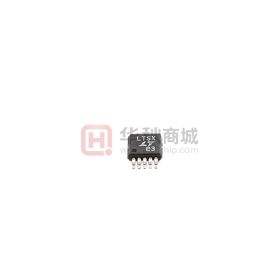
Small 10-Lead MSOP Package
APPLICATIONS
n
n
Telecom Power Supplies
Portable Electronic Equipment
The LTC®1871 is a wide input range, current mode, boost,
flyback or SEPIC controller that drives an N-channel power
MOSFET and requires very few external components. Intended for low to medium power applications, it eliminates
the need for a current sense resistor by utilizing the power
MOSFET’s on-resistance, thereby maximizing efficiency.
The IC’s operating frequency can be set with an external
resistor over a 50kHz to 1MHz range, and can be synchronized to an external clock using the MODE/SYNC
pin. Burst Mode operation at light loads, a low minimum
operating supply voltage of 2.5V and a low shutdown
quiescent current of 10μA make the LTC1871 ideally suited
for battery-operated systems.
For applications requiring constant frequency operation, Burst Mode operation can be defeated using the
MODE/SYNC pin. Higher output voltage boost, SEPIC
and flyback applications are possible with the LTC1871
by connecting the SENSE pin to a resistor in the source
of the power MOSFET.
The LTC1871 is available in the 10-lead MSOP package.
L, LT, LTC, LTM and Burst Mode are registered trademarks of Linear Technology Corporation.
No RSENSE is a trademark of Linear Technology Corporation. All other trademarks are the
property of their respective owners.
TYPICAL APPLICATION
VIN
3.3V
Efficiency of Figure 1
L1
1μH
100
D1
CC2
47pF
R2
37.4k
1%
+
LTC1871
R1
12.1k
1%
FB
FREQ
RT
80.6k
1%
MODE/SYNC
INTVCC
GATE
GND
CVCC
4.7μF
X5R
+
CIN
22μF
6.3V
×2
M1
COUT1
150μF
6.3V
×4
COUT2
22μF
6.3V
X5R
×2
GND
Burst Mode
OPERATION
80
EFFICIENCY (%)
CC1
6.8nF
VOUT
5V
7A
(10A PEAK)
VIN
ITH
RC
22k
90
SENSE
RUN
70
60
PULSE-SKIP
MODE
50
40
1871 F01a
CIN:
TAIYO YUDEN JMK325BJ226MM
COUT1: PANASONIC EEFUEOJ151R
COUT2: TAIYO YUDEN JMK325BJ226MM
D1: MBRB2515L
L1: SUMIDA CEP125-H 1R0MH
M1: FAIRCHILD FDS7760A
30
0.001
0.1
1
0.01
OUTPUT CURRENT (A)
10
1871 F01b
Figure 1. High Efficiency 3.3V Input, 5V Output Boost Converter (Bootstrapped)
1871fe
1
�LTC1871
ABSOLUTE MAXIMUM RATINGS
PIN CONFIGURATION
(Note 1)
TOP VIEW
VIN Voltage ............................................... – 0.3V to 36V
INTVCC Voltage............................................ –0.3V to 7V
INTVCC Output Current .......................................... 50mA
GATE Voltage ............................ –0.3V to VINTVCC + 0.3V
ITH, FB Voltages ....................................... –0.3V to 2.7V
RUN, MODE/SYNC Voltages ....................... –0.3V to 7V
FREQ Voltage ............................................ –0.3V to 1.5V
SENSE Pin Voltage .................................... –0.3V to 36V
Operating Temperature Range (Note 2)
LTC1871E............................................. –40°C to 85°C
LTC1871I............................................ –40°C to 125°C
LTC1871H .......................................... –40°C to 150°C
Junction Temperature (Note 3)
LTC1871E/LTC1871I ......................................... 125°C
LTC1871H ......................................................... 150°C
Storage Temperature Range................... –65°C to 150°C
Lead Temperature (Soldering, 10 sec) .................. 300°C
RUN
ITH
FB
FREQ
MODE/
SYNC
1
2
3
4
5
10
9
8
7
6
SENSE
VIN
INTVCC
GATE
GND
MS PACKAGE
10-LEAD PLASTIC MSOP
TJMAX = 125°C, θJA = 120°C/W
ORDER INFORMATION
LEAD FREE FINISH
TAPE AND REEL
PART MARKING
PACKAGE DESCRIPTION
TEMPERATURE RANGE
LTC1871EMS#PBF
LTC1871EMS#TRPBF
LTSX
10-Lead Plastic MSOP
–40°C to 85°C
LTC1871IMS#PBF
LTC1871IMS#TRPBF
LTBFC
10-Lead Plastic MSOP
–40°C to 125°C
LTC1871HMS#PBF
LTC1871HMS#TRPBF
LTCXS
10-Lead Plastic MSOP
–40°C to 150°C
LEAD BASED FINISH
TAPE AND REEL
PART MARKING
PACKAGE DESCRIPTION
TEMPERATURE RANGE
LTC1871EMS
LTC1871EMS#TR
LTSX
10-Lead Plastic MSOP
–40°C to 85°C
LTC1871IMS
LTC1871IMS#TR
LTBFC
10-Lead Plastic MSOP
–40°C to 125°C
LTC1871HMS
LTC1871HMS#TR
LTCXS
10-Lead Plastic MSOP
–40°C to 150°C
Consult LTC Marketing for parts specified with wider operating temperature ranges.
For more information on lead free part marking, go to: http://www.linear.com/leadfree/
For more information on tape and reel specifications, go to: http://www.linear.com/tapeandreel/
1871fe
2
�LTC1871
ELECTRICAL CHARACTERISTICS
The l denotes the specifications which apply over the full operating
temperature range, otherwise specifications are at TA = 25°C. VIN = VINTVCC = 5V, VRUN = 1.5V, RFREQ = 80k, VMODE/SYNC = 0V, unless
otherwise specified.
SYMBOL
PARAMETER
CONDITIONS
MIN
TYP
MAX
UNITS
Main Control Loop
VIN(MIN)
Minimum Input Voltage
IQ
Input Voltage Supply Current
(Note 4)
Continuous Mode
VMODE/SYNC = 5V, VFB = 1.4V, VITH = 0.75V
I-Grade or H-Grade (Note 2)
VMODE/SYNC = 5V, VFB = 1.4V, VITH = 0.75V,
I-Grade or H-Grade (Note 2)
Burst Mode Operation, No Load
Rising RUN Input Threshold Voltage
VRUN–
Falling RUN Input Threshold Voltage
VRUN(HYST)
RUN Pin Input Threshold Hysteresis
550
1000
μA
250
500
μA
●
250
500
μA
10
20
μA
●
10
20
μA
1.273
1.298
V
V
●
1.223
1.198
●
1.179
100
FB Pin Input Current
VITH = 0.2V (Note 5)
ΔVFB
Line Regulation
2.5V ≤ VIN ≤ 30V
VITH = 0.2V (Note 5), I-Grade or H-Grade (Note 2)
●
1.218
1.212
●
1.205
V
1.315
100
35
VITH = 0.2V (Note 5)
1.248
50
35
IFB
ΔFB Pin, Overvoltage Lockout
●
●
Feedback Voltage
ΔVFB(OV)
μA
●
VFB
ΔVITH
1000
H-Grade (Note 2)
RUN Input Current
Load Regulation
550
I-Grade (Note 2)
IRUN
ΔVFB
V
1.348
H-Grade (Note 2)
ΔVIN
2.5
VRUN = 0V
VRUN = 0V, I-Grade or H-Grade (Note 2)
VRUN+
V
VMODE/SYNC = 0V, VITH = 0.2V (Note 5)
VMODE/SYNC = 0V, VITH = 0.2V (Note 5),
I-Grade or H-Grade (Note 2)
Shutdown Mode
●
2.5
150
V
mV
175
mV
300
mV
1
60
nA
1.230
1.242
1.248
V
V
1.255
V
18
60
nA
0.002
0.02
%/V
0.002
0.02
%/V
2.5V ≤ VIN ≤ 30V, I-Grade or H-Grade (Note 2)
●
VMODE/SYNC = 0V, VITH = 0.5V to 0.9V (Note 5)
●
–1
–0.1
%
VMODE/SYNC = 0V, VITH = 0.5V to 0.9V (Note 5)
I-Grade or H-Grade (Note 2)
●
–1
–0.1
%
2.5
6
VFB(OV) – VFB(NOM) in Percent
10
%
gm
Error Amplifier Transconductance
ITH Pin Load = ±5μA (Note 5)
650
μmho
VITH(BURST)
Burst Mode Operation ITH Pin Voltage
Falling ITH Voltage (Note 5)
0.3
V
VSENSE(MAX)
Maximum Current Sense Input Threshold
Duty Cycle < 20%
ISENSE(ON)
SENSE Pin Current (GATE High)
VSENSE = 0V
35
ISENSE(OFF)
SENSE Pin Current (GATE Low)
VSENSE = 30V
Oscillator Frequency
RFREQ = 80k
Duty Cycle < 20%, I-Grade or H-Grade (Note 2)
120
●
150
180
mV
200
mV
50
μA
0.1
5
μA
250
300
350
kHz
100
Oscillator
fOSC
RFREQ = 80k, I-Grade (Note 2)
●
250
300
350
kHz
RFREQ = 80k, H-Grade (Note 2)
●
240
300
360
kHz
50
1000
kHz
50
1000
kHz
Oscillator Frequency Range
I-Grade or H-Grade (Note 2)
●
1871fe
3
�LTC1871
ELECTRICAL CHARACTERISTICS
The l denotes the specifications which apply over the full operating
temperature range, otherwise specifications are at TA = 25°C. VIN = VINTVCC = 5V, VRUN = 1.5V, RFREQ = 80k, VMODE/SYNC = 0V, unless
otherwise specified.
SYMBOL
PARAMETER
DMAX
Maximum Duty Cycle
CONDITIONS
I-Grade or H-Grade (Note 2)
fSYNC/fOSC
Recommended Maximum Synchronized
Frequency Ratio
fOSC = 300kHz (Note 6)
tSYNC(MIN)
MODE/SYNC Minimum Input Pulse Width
VSYNC = 0V to 5V
tSYNC(MAX)
MODE/SYNC Maximum Input Pulse Width VSYNC = 0V to 5V
VIL(MODE)
Low Level MODE/SYNC Input Voltage
VIH(MODE)
fOSC = 300kHz (Note 6), I-Grade or H-Grade (Note 2)
●
MODE/SYNC Input Pull-Down Resistance
VFREQ
Nominal FREQ Pin Voltage
TYP
MAX
87
92
97
%
87
92
97
%
1.25
1.30
1.25
1.30
●
I-Grade or H-Grade (Note 2)
●
I-Grade or H-Grade (Note 2)
●
High Level MODE/SYNC Input Voltage
RMODE/SYNC
MIN
UNITS
25
ns
0.8/fOSC
ns
0.3
V
0.3
V
1.2
V
1.2
V
50
kΩ
0.62
V
Low Dropout Regulator
VINTVCC
INTVCC Regulator Output Voltage
VIN = 7.5V
5.0
5.2
5.4
V
VIN = 7.5V, I-Grade (Note 2)
●
5.0
5.2
5.4
V
VIN = 7.5V, H-Grade (Note 2)
●
4.95
5.2
5.45
V
ΔVINTVCC
INTVCC Regulator Line Regulation
7.5V ≤ VIN ≤ 15V
8
25
mV
ΔVIN1
ΔVINTVCC
INTVCC Regulator Line Regulation
15V ≤ VIN ≤ 30V
70
200
mV
ΔVIN2
VLDO(LOAD)
INTVCC Load Regulation
0 ≤ IINTVCC ≤ 20mA, VIN = 7.5V
–0.2
%
VDROPOUT
INTVCC Regulator Dropout Voltage
VIN = 5V, INTVCC Load = 20mA
–2
280
mV
IINTVCC
Bootstrap Mode INTVCC Supply
Current in Shutdown
RUN = 0V, SENSE = 5V
10
20
μA
I-Grade (Note 2)
●
30
μA
H-Grade (Note 2)
●
50
μA
GATE Driver
tr
GATE Driver Output Rise Time
CL = 3300pF (Note 7)
17
100
ns
tf
GATE Driver Output Fall Time
CL = 3300pF (Note 7)
8
100
ns
Note 1: Stresses beyond those listed under Absolute Maximum Ratings
may cause permanent damage to the device. Exposure to any Absolute
Maximum Rating condition for extended periods may affect device
reliability and lifetime.
Note 2: The LTC1871E is guaranteed to meet performance specifications
from 0°C to 85°C operating temperature. Specifications over the – 40°C to
85°C operating temperature range are assured by design, characterization
and correlation with statistical process controls. The LTC1871I is
guaranteed over the full –40°C to 125°C operating temperature range
and the LTC1871H is guaranteed over the full –40°C to 150°C operating
temperature range.
Note 3: TJ is calculated from the ambient temperature TA and power
dissipation PD according to the following formula:
TJ = TA + (PD • 110°C/W)
Note 4: The dynamic input supply current is higher due to power MOSFET
gate charging (QG • fOSC). See Applications Information.
Note 5: The LTC1871 is tested in a feedback loop which servos VFB to
the reference voltage with the ITH pin forced to the midpoint of its voltage
range (0.3V ≤ VITH ≤ 1.2V, midpoint = 0.75V).
Note 6: In a synchronized application, the internal slope compensation
gain is increased by 25%. Synchronizing to a significantly higher ratio will
reduce the effective amount of slope compensation, which could result in
subharmonic oscillation for duty cycles greater than 50%.
Note 7: Rise and fall times are measured at 10% and 90% levels.
1871fe
4
�LTC1871
TYPICAL PERFORMANCE CHARACTERISTICS
FB Voltage vs Temp
FB Voltage Line Regulation
FB Pin Current vs Temperature
60
1.231
1.25
50
1.23
FB PIN CURRENT (nA)
FB VOLTAGE (V)
FB VOLTAGE (V)
1.24
1.230
40
30
20
1.22
10
1.21
–50 –25
0
–50 –25
1.229
0
0
25 50 75 100 125 150
TEMPERATURE (°C)
5
10
15
20
VIN (V)
25
30
35
25 50 75 100 125 150
TEMPERATURE (°C)
0
1871 G03
1871 G02
1871 G01
Shutdown Mode IQ vs VIN
Shutdown Mode IQ vs Temperature
20
30
Burst Mode IQ vs VIN
600
VIN = 5V
20
10
Burst Mode IQ (μA)
SHUTDOWN MODE IQ (μA)
SHUTDOWN MODE IQ (μA)
500
15
10
400
300
200
5
100
0
0
10
20
VIN (V)
30
0
–50 –25
40
0
1871 G04
10
0
20
VIN (V)
30
1871 G05
Burst Mode IQ vs Temperature
18
Gate Drive Rise and
Fall Time vs CL
60
CL = 3300pF
IQ(TOT) = 550μA + Qg • f
16
40
1871 G06
Dynamic IQ vs Frequency
500
50
400
14
12
200
40
TIME (ns)
300
IQ (mA)
Burst Mode IQ (μA)
0
25 50 75 100 125 150
TEMPERATURE (°C)
10
8
6
RISE TIME
30
20
FALL TIME
4
100
10
2
0
–50 –25
0
25 50 75 100 125 150
TEMPERATURE (°C)
1871 G07
0
0
0
200
400
800
600
FREQUENCY (kHz)
1000
1200
1871 G08
0
2000
4000
6000 8000
CL (pF)
10000 12000
1871 G09
1871fe
5
�LTC1871
TYPICAL PERFORMANCE CHARACTERISTICS
RUN Thresholds vs VIN
RUN Thresholds vs Temperature
RT vs Frequency
1000
1.40
1.4
1.3
1.2
10
0
20
VIN (V)
30
1.35
RT (kΩ)
RUN THRESHOLDS (V)
RUN THRESHOLDS (V)
1.5
1.30
1.25
1.20
–50 –25
40
100
0
10
25 50 75 100 125 150
TEMPERATURE (°C)
1871 G10
1871 G12
1871 G11
SENSE Pin Current
vs Temperature
Maximum Sense Threshold
vs Temperature
Frequency vs Temperature
325
35
160
GATE HIGH
VSENSE = 0V
GATE FREQUENCY (kHz)
310
305
300
295
290
285
SENSE PIN CURRENT (μA)
MAX SENSE THRESHOLD (mV)
320
315
0 100 200 300 400 500 600 700 800 900 1000
FREQUENCY (kHz)
155
150
145
30
280
275
–50 –25
0
140
–50 –25
25 50 75 100 125 150
TEMPERATURE (°C)
0
1871 G13
0
25 50 75 100 125 150
TEMPERATURE (°C)
1871 G15
1871 G14
INTVCC Load Regulation
INTVCC Dropout Voltage
vs Current, Temperature
INTVCC Line Regulation
500
5.4
VIN = 7.5V
450
5.1
DROPOUT VOLTAGE (mV)
INTVCC VOLTAGE (V)
5.2
INTVCC VOLTAGE (V)
25
–50 –25
25 50 75 100 125 150
TEMPERATURE (°C)
5.3
5.2
150°C
400
125°C
350
75°C
300
25°C
250
200
0°C
150
–50°C
100
50
5.0
5.1
0
10
20
30 40
50 60
INTVCC LOAD (mA)
70
80
1871 G16
0
5
10
15
20 25
VIN (V)
30
0
35
40
1871 G17
0
5
10
15
INTVCC LOAD (mA)
20
1871 G18
1871fe
6
�LTC1871
PIN FUNCTIONS
RUN (Pin 1): The RUN pin provides the user with an
accurate means for sensing the input voltage and programming the start-up threshold for the converter. The
falling RUN pin threshold is nominally 1.248V and the
comparator has 100mV of hysteresis for noise immunity.
When the RUN pin is below this input threshold, the IC
is shut down and the VIN supply current is kept to a low
value (typ 10μA). The Absolute Maximum Rating for the
voltage on this pin is 7V.
operating frequency to an external clock. If the MODE/
SYNC pin is connected to ground, Burst Mode operation
is enabled. If the MODE/SYNC pin is connected to INTVCC,
or if an external logic-level synchronization signal is applied to this input, Burst Mode operation is disabled and
the IC operates in a continuous mode.
ITH (Pin 2): Error Amplifier Compensation Pin. The
current comparator input threshold increases with this
control voltage. Nominal voltage range for this pin is 0V
to 1.40V.
INTVCC (Pin 8): The Internal 5.20V Regulator Output.
The gate driver and control circuits are powered from
this voltage. Decouple this pin locally to the IC ground
with a minimum of 4.7μF low ESR tantalum or ceramic
capacitor.
FB (Pin 3): Receives the feedback voltage from the external
resistor divider across the output. Nominal voltage for
this pin in regulation is 1.230V.
VIN (Pin 9): Main Supply Pin. Must be closely decoupled
to ground.
FREQ (Pin 4): A resistor from the FREQ pin to ground
programs the operating frequency of the chip. The nominal
voltage at the FREQ pin is 0.6V.
MODE/SYNC (Pin 5): This input controls the operating
mode of the converter and allows for synchronizing the
GND (Pin 6): Ground Pin.
GATE (Pin 7): Gate Driver Output.
SENSE (Pin 10): The Current Sense Input for the Control
Loop. Connect this pin to the drain of the power MOSFET
for VDS sensing and highest efficiency. Alternatively, the
SENSE pin may be connected to a resistor in the source
of the power MOSFET. Internal leading edge blanking is
provided for both sensing methods.
1871fe
7
�LTC1871
BLOCK DIAGRAM
RUN
+
BIAS AND
START-UP
CONTROL
SLOPE
COMPENSATION
1
C2
–
1.248V
VIN
FREQ
V-TO-I
4
OSC
9
0.6V
IOSC
MODE/SYNC
INTVCC
5
85mV
+
1.230V
50k
S
Q
GND
R
+
0.30V
FB
–
3
1.230V
+
7
LOGIC
OV
–
GATE
PWM LATCH
EA
+
BURST
COMPARATOR
CURRENT
COMPARATOR
SENSE
+
10
C1
–
–
gm
ITH
V-TO-I
2
INTVCC
8
5.2V
ILOOP
LDO
RLOOP
1.230V
SLOPE
1.230V
–
2.00V
+
UV
TO
START-UP
CONTROL
GND
BIAS
VREF
6
1871 BD
VIN
OPERATION
Main Control Loop
The LTC1871 is a constant frequency, current mode controller for DC/DC boost, SEPIC and flyback converter applications. The LTC1871 is distinguished from conventional
current mode controllers because the current control loop
can be closed by sensing the voltage drop across the power
MOSFET switch instead of across a discrete sense resistor,
as shown in Figure 2. This sensing technique improves
efficiency, increases power density, and reduces the cost
of the overall solution.
For circuit operation, please refer to the Block Diagram of
the IC and Figure 1. In normal operation, the power MOSFET
is turned on when the oscillator sets the PWM latch and
is turned off when the current comparator C1 resets the
latch. The divided-down output voltage is compared to an
internal 1.230V reference by the error amplifier EA, which
outputs an error signal at the ITH pin. The voltage on the
ITH pin sets the current comparator C1 input threshold.
When the load current increases, a fall in the FB voltage
relative to the reference voltage causes the ITH pin to rise,
which causes the current comparator C1 to trip at a higher
peak inductor current value. The average inductor current
will therefore rise until it equals the load current, thereby
maintaining output regulation.
1871fe
8
�LTC1871
OPERATION
L
D
VIN
VOUT
VIN
+
SENSE
COUT
VSW
GATE
GND
GND
2a. SENSE Pin Connection for
Maximum Efficiency (VSW < 36V)
L
D
VIN
VOUT
VIN
VSW
GATE
reset pulse to the main RS latch. Because this RS latch is
reset-dominant, the power MOSFET is actively held off for
the duration of an output overvoltage condition.
The LTC1871 can be used either by sensing the voltage
drop across the power MOSFET or by connecting the
SENSE pin to a conventional shunt resistor in the source
of the power MOSFET, as shown in Figure 2. Sensing the
voltage across the power MOSFET maximizes converter
efficiency and minimizes the component count, but limits
the output voltage to the maximum rating for this pin (36V).
By connecting the SENSE pin to a resistor in the source
of the power MOSFET, the user is able to program output
voltages significantly greater than 36V.
+
SENSE
GND
GND
COUT
RS
1871 F02
2b. SENSE Pin Connection for Precise
Control of Peak Current or for VSW > 36V
Figure 2. Using the SENSE Pin On the LTC1871
The nominal operating frequency of the LTC1871 is programmed using a resistor from the FREQ pin to ground
and can be controlled over a 50kHz to 1000kHz range. In
addition, the internal oscillator can be synchronized to
an external clock applied to the MODE/SYNC pin and can
be locked to a frequency between 100% and 130% of its
nominal value. When the MODE/SYNC pin is left open, it
is pulled low by an internal 50k resistor and Burst Mode
operation is enabled. If this pin is taken above 2V or an
external clock is applied, Burst Mode operation is disabled
and the IC operates in continuous mode. With no load (or
an extremely light load), the controller will skip pulses in
order to maintain regulation and prevent excessive output
ripple.
The RUN pin controls whether the IC is enabled or is in a low
current shutdown state. A micropower 1.248V reference
and comparator C2 allow the user to program the supply
voltage at which the IC turns on and off (comparator C2
has 100mV of hysteresis for noise immunity). With the
RUN pin below 1.248V, the chip is off and the input supply
current is typically only 10μA.
An overvoltage comparator OV senses when the FB pin
exceeds the reference voltage by 6.5% and provides a
Programming the Operating Mode
For applications where maximizing the efficiency at very
light loads (e.g., 1μF) supply bypass capacitors.
The discharged bypass capacitors are effectively put in
parallel with CO, causing a nearly instantaneous drop in
VO. No regulator can deliver enough current to prevent
this problem if the load switch resistance is low and it is
driven quickly. The only solution is to limit the rise time
of the switch drive in order to limit the inrush current
di/dt to the load.
Boost Converter Design Example
The design example given here will be for the circuit shown
in Figure 1. The input voltage is 3.3V, and the output is 5V
at a maximum load current of 7A (10A peak).
1. The duty cycle is:
� V + V – V � 5 + 0.4 – 3.3
D = � O D IN � =
= 38.9%
5 + 0.4
� VO + VD �
2. Pulse-skip operation is chosen so the MODE/SYNC pin
is shorted to INTVCC.
3. The operating frequency is chosen to be 300kHz to
reduce the size of the inductor. From Figure 5, the
resistor from the FREQ pin to ground is 80k.
4. An inductor ripple current of 40% of the maximum load
current is chosen, so the peak input current (which is
also the minimum saturation current) is:
7
� � � IO(MAX)
IIN(PEAK) = �1+ � •
= 1.2 •
= 13.8A
� 2 � 1– DMAX
1– 0.39
The inductor ripple current is:
�IL = � •
IO(MAX)
1– DMAX
= 0.4 •
7
= 4.6A
1– 0.39
And so the inductor value is:
VIN(MIN)
3.3V
L=
• DMAX =
• 0.39 = 0.93μH
�IL • f
4.6A • 300kHz
The component chosen is a 1μH inductor made by
Sumida (part number CEP125-H 1ROMH) which has
a saturation current of greater than 20A.
5. With the input voltage to the IC bootstrapped to the
output of the power supply (5V), a logic-level MOSFET
can be used. Because the duty cycle is 39%, the maximum SENSE pin threshold voltage is reduced from its
low duty cycle typical value of 150mV to approximately
140mV. Assuming a MOSFET junction temperature of
125°C, the room temperature MOSFET RDS(ON) should
be less than:
1– DMAX
� ��
�� 1+ 2
•IO(MAX) • �T
1– 0.39
= 6.8m�
= 0.140V •
� 0.4 �
�� 1+ 2
• 7A • 1.5
RDS(ON) � VSENSE(MAX) •
The MOSFET used was the Fairchild FDS7760A, which
has a maximum RDS(ON) of 8mΩ at 4.5V VGS, a BVDSS
of greater than 30V, and a gate charge of 37nC at 5V
VGS.
6. The diode for this design must handle a maximum
DC output current of 10A and be rated for a minimum
reverse voltage of VOUT, or 5V. A 25A, 15V diode from
On Semiconductor (MBRB2515L) was chosen for its
high power dissipation capability.
7. The output capacitor usually consists of a high valued
bulk C connected in parallel with a lower valued, low
ESR ceramic. Based on a maximum output ripple voltage
of 1%, or 50mV, the bulk C needs to be greater than:
COUT �
IOUT(MAX)
0.01• VOUT • f
=
7A
= 466μF
0.01• 5V • 300kHz
The RMS ripple current rating for this capacitor needs
to exceed:
IRMS(COUT) �IO(MAX) •
7A •
VO – VIN(MIN)
VIN(MIN)
=
5V – 3.3V
= 5A
3.3V
To satisfy this high RMS current demand, four
150μF Panasonic capacitors (EEFUEOJ151R) are
required. In parallel with these bulk capacitors, two
22μF, low ESR (X5R) Taiyo Yuden ceramic capacitors
1871fe
21
�LTC1871
APPLICATIONS INFORMATION
(JMK325BJ226MM) are added for HF noise reduction.
Check the output ripple with a single oscilloscope
probe connected directly across the output capacitor
terminals, where the HF switching currents flow.
8. The choice of an input capacitor for a boost converter
depends on the impedance of the source supply and
the amount of input ripple the converter will safely tolerate. For this particular design and lab setup a 100μF
Sanyo Poscap (6TPC 100M), in parallel with two 22μF
Taiyo Yuden ceramic capacitors (JMK325BJ226MM)
is required (the input and return lead lengths are kept
to a few inches, but the peak input current is close to
20A!). As with the output node, check the input ripple
with a single oscilloscope probe connected across the
input capacitor terminals.
PC Board Layout Checklist
1. In order to minimize switching noise and improve output
load regulation, the GND pin of the LTC1871 should be
connected directly to 1) the negative terminal of the
INTVCC decoupling capacitor, 2) the negative terminal
of the output decoupling capacitors, 3) the source of
the power MOSFET or the bottom terminal of the sense
resistor, 4) the negative terminal of the input capacitor
and 5) at least one via to the ground plane immediately
adjacent to Pin 6. The ground trace on the top layer of
the PC board should be as wide and short as possible
to minimize series resistance and inductance.
should be kept as tight as possible to reduce inductive
ringing. Excess inductance can cause increased stress
on the power MOSFET and increase HF noise on the
output. If low ESR ceramic capacitors are used on the
output to reduce output noise, place these capacitors
close to the boost diode in order to keep the series
inductance to a minimum.
5. Check the stress on the power MOSFET by measuring
its drain-to-source voltage directly across the device
terminals (reference the ground of a single scope probe
directly to the source pad on the PC board). Beware
of inductive ringing which can exceed the maximum
specified voltage rating of the MOSFET. If this ringing
cannot be avoided and exceeds the maximum rating
of the device, either choose a higher voltage device
or specify an avalanche-rated power MOSFET. Not all
MOSFETs are created equal (some are more equal than
others).
6. Place the small-signal components away from high
frequency switching nodes. In the layout shown in
Figure 14, all of the small-signal components have
been placed on one side of the IC and all of the power
components have been placed on the other. This also
allows the use of a pseudo-Kelvin connection for the
signal ground, where high di/dt gate driver currents
flow out of the IC ground pin in one direction (to the
bottom plate of the INTVCC decoupling capacitor) and
small-signal currents flow in the other direction.
2. Beware of ground loops in multiple layer PC boards.
Try to maintain one central ground node on the board
and use the input capacitor to avoid excess input ripple
for high output current power supplies. If the ground
plane is to be used for high DC currents, choose a path
away from the small-signal components.
7. If a sense resistor is used in the source of the power
MOSFET, minimize the capacitance between the SENSE
pin trace and any high frequency switching nodes. The
LTC1871 contains an internal leading edge blanking time
of approximately 180ns, which should be adequate for
most applications.
3. Place the CVCC capacitor immediately adjacent to the
INTVCC and GND pins on the IC package. This capacitor carries high di/dt MOSFET gate drive currents. A
low ESR and ESL 4.7μF ceramic capacitor works well
here.
8. For optimum load regulation and true remote sensing,
the top of the output resistor divider should connect
independently to the top of the output capacitor (Kelvin
connection), staying away from any high dV/dt traces.
Place the divider resistors near the LTC1871 in order
to keep the high impedance FB node short.
4. The high di/dt loop from the bottom terminal of the
output capacitor, through the power MOSFET, through
the boost diode and back through the output capacitors
9. For applications with multiple switching power converters connected to the same input supply, make sure
1871fe
22
�LTC1871
APPLICATIONS INFORMATION
VIN
L1
JUMPER
R3
RC
R4
CC
J1
CIN
PIN 1
R2
LTC1871
R1
RT
CVCC
PSEUDO-KELVIN
SIGNAL GROUND
CONNECTION
SWITCH NODE IS ALSO
THE HEAT SPREADER
FOR L1, M1, D1
M1
COUT
COUT
D1
VIAS TO GROUND
PLANE
VOUT
TRUE REMOTE
OUTPUT SENSING
BULK C
1871 F14
LOW ESR CERAMIC
Figure 14. LTC1871 Boost Converter Suggested Layout
VIN
R3
CC
R1
R2
R4
1
RC
2
SENSE
VIN
ITH
10
SWITCH
NODE
9
LTC1871
3
4
RT
RUN
L1
J1
5
FB
FREQ
INTVCC
GATE
MODE/
SYNC
GND
D1
8
7
M1
6
+
CVCC
CIN
GND
+
PSEUDO-KELVIN
GROUND CONNECTION
COUT
BOLD LINES INDICATE HIGH CURRENT PATHS
VOUT
1871 F15
Figure 15. LTC1871 Boost Converter Layout Diagram
1871fe
23
�LTC1871
APPLICATIONS INFORMATION
that the input filter capacitor for the LTC1871 is not
shared with other converters. AC input current from
another converter could cause substantial input voltage
ripple, and this could interfere with the operation of the
LTC1871. A few inches of PC trace or wire (L ≈ 100nH)
between the CIN of the LTC1871 and the actual source
VIN should be sufficient to prevent current sharing
problems.
SEPIC Converter Applications
The LTC1871 is also well suited to SEPIC (single-ended
primary inductance converter) converter applications. The
SEPIC converter shown in Figure 16 uses two inductors.
The advantage of the SEPIC converter is the input voltage
may be higher or lower than the output voltage, and the
output is short-circuit protected.
C1
L1
VIN
D1
+
+
•
SW
VOUT
+
L2
RL
COUT
•
VIN
VOUT
+
+
+
VIN
RL
•
16b. Current Flow During Switch On-Time
VIN
D1
+
+
•
VOUT
+
VIN
SEPIC Converter: Duty Cycle Considerations
For a SEPIC converter operating in a continuous conduction
mode (CCM), the duty cycle of the main switch is:
� VO + VD �
D= �
� VIN + VO + VD ��
where VD is the forward voltage of the diode. For converters where the input voltage is close to the output voltage
the duty cycle is near 50%.
The maximum output voltage for a SEPIC converter is:
VO(MAX) = ( VIN + VD )
DMAX
1
– VD
1– DMAX
1– DMAX
The maximum duty cycle of the LTC1871 is typically
92%.
SEPIC Converter: The Peak and Average Input
Currents
16a. SEPIC Topology
•
and size. All of the SEPIC applications information that
follows assumes L1 = L2 = L.
RL
•
16c. Current Flow During Switch Off-Time
Figures 16. SEPIC Topology and Current Flow
The first inductor, L1, together with the main switch,
resembles a boost converter. The second inductor, L2,
together with the output diode D1, resembles a flyback or
buck-boost converter. The two inductors L1 and L2 can be
independent but can also be wound on the same core since
identical voltages are applied to L1 and L2 throughout the
switching cycle. By making L1 = L2 and winding them on
the same core the input ripple is reduced along with cost
The control circuit in the LTC1871 is measuring the input
current (either using the RDS(ON) of the power MOSFET
or by means of a sense resistor in the MOSFET source),
so the output current needs to be reflected back to the
input in order to dimension the power MOSFET properly.
Based on the fact that, ideally, the output power is equal
to the input power, the maximum input current for a SEPIC
converter is:
D
IIN(MAX) =IO(MAX) • MAX
1– DMAX
The peak input current is:
D
� ��
IIN(PEAK) = � 1+ � •IO(MAX) • MAX
� 2�
1– DMAX
The maximum duty cycle, DMAX, should be calculated at
minimum VIN.
The constant ‘χ’ represents the fraction of ripple current in
the inductor relative to its maximum value. For example, if
30% ripple current is chosen, then χ = 0.30 and the peak
current is 15% greater than the average.
1871fe
24
�LTC1871
APPLICATIONS INFORMATION
It is worth noting here that SEPIC converters that operate
at high duty cycles (i.e., that develop a high output voltage from a low input voltage) can have very high input
currents, relative to the output current. Be sure to check
that the maximum load current will not overload the input
supply.
SEPIC Converter: Inductor Selection
For most SEPIC applications the equal inductor values
will fall in the range of 10μH to 100μH. Higher values will
reduce the input ripple voltage and reduce the core loss.
Lower inductor values are chosen to reduce physical size
and improve transient response.
Like the boost converter, the input current of the SEPIC
converter is calculated at full load current and minimum
input voltage. The peak inductor current can be significantly
higher than the output current, especially with smaller inductors and lighter loads. The following formulas assume
CCM operation and calculate the maximum peak inductor
currents at minimum VIN:
V +V
� ��
IL1(PEAK) = � 1+ � •IO(MAX) • O D
� 2�
VIN(MIN)
VIN(MIN) + VD
� ��
IL2(PEAK) = � 1+ � •IO(MAX) •
� 2�
VIN(MIN)
The ripple current in the inductor is typically 20% to 40%
(i.e., a range of ‘χ’ from 0.20 to 0.40) of the maximum
average input current occurring at VIN(MIN) and IO(MAX) and
ΔIL1 = ΔIL2. Expressing this ripple current as a function of
the output current results in the following equations for
calculating the inductor value:
L=
VIN(MIN)
�IL • f
• DMAX
where:
�IL = � •IO(MAX) •
DMAX
1– DMAX
By making L1 = L2 and winding them on the same core,
the value of inductance in the equation above is replace
by 2L due to mutual inductance. Doing this maintains the
same ripple current and energy storage in the inductors. For
example, a Coiltronix CTX10-4 is a 10μH inductor with two
windings. With the windings in parallel, 10μH inductance is
obtained with a current rating of 4A (the number of turns
hasn’t changed, but the wire diameter has doubled). Splitting the two windings creates two 10μH inductors with a
current rating of 2A each. Therefore, substituting 2L yields
the following equation for coupled inductors:
VIN(MIN)
L1= L2 =
•D
2 • �IL • f MAX
Specify the maximum inductor current to safely handle
IL(PK) specified in the equation above. The saturation
current rating for the inductor should be checked at the
minimum input voltage (which results in the highest
inductor current) and maximum output current.
SEPIC Converter: Power MOSFET Selection
The power MOSFET serves two purposes in the LTC1871:
it represents the main switching element in the power path,
and its RDS(ON) represents the current sensing element
for the control loop. Important parameters for the power
MOSFET include the drain-to-source breakdown voltage
(BVDSS), the threshold voltage (VGS(TH)), the on-resistance
(RDS(ON)) versus gate-to-source voltage, the gate-to-source
and gate-to-drain charges (QGS and QGD, respectively),
the maximum drain current (ID(MAX)) and the MOSFET’s
thermal resistances (RTH(JC) and RTH(JA)).
The gate drive voltage is set by the 5.2V INTVCC low
dropout regulator. Consequently, logic-level threshold
MOSFETs should be used in most LTC1871 applications.
If low input voltage operation is expected (e.g., supplying
power from a lithium-ion battery), then sublogic-level
threshold MOSFETs should be used.
The maximum voltage that the MOSFET switch must
sustain during the off-time in a SEPIC converter is equal
to the sum of the input and output voltages (VO + VIN).
As a result, careful attention must be paid to the BVDSS
specifications for the MOSFETs relative to the maximum
actual switch voltage in the application. Many logic-level
devices are limited to 30V or less. Check the switching
waveforms directly across the drain and source terminals
of the power MOSFET to ensure the VDS remains below
the maximum rating for the device.
1871fe
25
�LTC1871
APPLICATIONS INFORMATION
During the MOSFET’s on-time, the control circuit limits
the maximum voltage drop across the power MOSFET to
about 150mV (at low duty cycle). The peak inductor current
is therefore limited to 150mV/RDS(ON). The relationship
between the maximum load current, duty cycle and the
RDS(ON) of the power MOSFET is:
RDS(ON) �
VSENSE(MAX)
IO(MAX)
•
1
1
•
�V +V �
� ��
�� 1+ 2 � • �T � O D � + 1
� VIN(MIN)
The VSENSE(MAX) term is typically 150mV at low duty cycle
and is reduced to about 100mV at a duty cycle of 92% due
to slope compensation, as shown in Figure 8. The constant
‘χ’ in the denominator represents the ripple current in the
inductors relative to their maximum current. For example,
if 30% ripple current is chosen, then χ = 0.30. The ρT term
accounts for the temperature coefficient of the RDS(ON) of
the MOSFET, which is typically 0.4%/°C. Figure 9 illustrates
the variation of normalized RDS(ON) over temperature for
a typical power MOSFET.
Another method of choosing which power MOSFET to
use is to check what the maximum output current is for a
given RDS(ON) since MOSFET on-resistances are available
in discrete values.
IO(MAX) �
VSENSE(MAX)
RDS(ON)
1
1
•
•
�
�V +V �
�
�
�� 1+ 2 � • �T � O D � + 1
� VIN(MIN)
Calculating Power MOSFET Switching and Conduction
Losses and Junction Temperatures
In order to calculate the junction temperature of the
power MOSFET, the power dissipated by the device must
be known. This power dissipation is a function of the
duty cycle, the load current and the junction temperature
itself. As a result, some iterative calculation is normally
required to determine a reasonably accurate value. Since
the controller is using the MOSFET as both a switching
and a sensing element, care should be taken to ensure
that the converter is capable of delivering the required
load current over all operating conditions (load, line and
temperature) and for the worst-case specifications for
VSENSE(MAX) and the RDS(ON) of the MOSFET listed in the
manufacturer’s data sheet.
The power dissipated by the MOSFET in a SEPIC converter
is:
2
�
�
D
PFET = � IO(MAX) • MAX � • RDS(ON) • DMAX • �T
1– DMAX �
�
(
+ k • VIN(MIN) + VO
•C
•f
)1.85 •IO(MAX) • 1–DMAX
DMAX RSS
The first term in the equation above represents the I2R
losses in the device and the second term, the switching
losses. The constant k = 1.7 is an empirical factor inversely
related to the gate drive current and has the dimension
of 1/current.
From a known power dissipated in the power MOSFET, its
junction temperature can be obtained using the following
formula:
TJ = TA + PFET •RTH(JA)
The RTH(JA) to be used in this equation normally includes
the RTH(JC) for the device plus the thermal resistance from
the board to the ambient temperature in the enclosure.
This value of TJ can then be used to check the original
assumption for the junction temperature in the iterative
calculation process.
SEPIC Converter: Output Diode Selection
To maximize efficiency, a fast-switching diode with low
forward drop and low reverse leakage is desired. The output
diode in a SEPIC converter conducts current during the
switch off-time. The peak reverse voltage that the diode
must withstand is equal to VIN(MAX) + VO. The average
forward current in normal operation is equal to the output
current, and the peak current is equal to:
�V +V
�
� ��
ID(PEAK) = � 1+ � •IO(MAX) • � O D + 1�
�
2�
� VIN(MIN) �
The power dissipated by the diode is:
PD = IO(MAX) • VD
and the diode junction temperature is:
TJ = TA + PD • RTH(JA)
The RTH(JA) to be used in this equation normally includes
the RTH(JC) for the device plus the thermal resistance from
the board to the ambient temperature in the enclosure.
1871fe
26
�LTC1871
APPLICATIONS INFORMATION
SEPIC Converter: Output Capacitor Selection
Because of the improved performance of today’s electrolytic, tantalum and ceramic capacitors, engineers need
to consider the contributions of ESR (equivalent series
resistance), ESL (equivalent series inductance) and the
bulk capacitance when choosing the correct component
for a given output ripple voltage. The effects of these three
parameters (ESR, ESL, and bulk C) on the output voltage
ripple waveform are illustrated in Figure 17 for a typical
coupled-inductor SEPIC converter.
IL1
IIN
SW
ON
SW
OFF
For a 1% contribution to the total ripple voltage, the ESR
of the output capacitor can be determined using the following equation:
ESRCOUT �
17a. Input Inductor Current
IO
IL2
The choice of component(s) begins with the maximum
acceptable ripple voltage (expressed as a percentage of
the output voltage), and how this ripple should be divided
between the ESR step and the charging/discharging ΔV.
For the purpose of simplicity we will choose 2% for the
maximum output ripple, to be divided equally between the
ESR step and the charging/discharging ΔV. This percentage
ripple will change, depending on the requirements of the
application, and the equations provided below can easily
be modified.
0.01• VO
ID(PEAK)
where:
�V +V
�
� ��
ID(PEAK) = � 1+ � •IO(MAX) • � O D + 1�
� 2�
� VIN(MIN) �
17b. Output Inductor Current
IIN
For the bulk C component, which also contributes 1% to
the total ripple:
IC1
IO
17c. DC Coupling Capacitor Current
ID1
IO
17d. Diode Current
VOUT
(AC)
ΔVCOUT
ΔVESR
RINGING DUE TO
TOTAL INDUCTANCE
(BOARD + CAP)
17e. Output Ripple Voltage
Figure 17. SEPIC Converter Switching Waveforms
COUT �
IO(MAX)
0.01• VO • f
For many designs it is possible to choose a single capacitor
type that satisfies both the ESR and bulk C requirements
for the design. In certain demanding applications, however,
the ripple voltage can be improved significantly by connecting two or more types of capacitors in parallel. For
example, using a low ESR ceramic capacitor can minimize
the ESR step, while an electrolytic or tantalum capacitor
can be used to supply the required bulk C.
Once the output capacitor ESR and bulk capacitance have
been determined, the overall ripple voltage waveform
should be verified on a dedicated PC board (see Board
Layout section for more information on component placement). Lab breadboards generally suffer from excessive
series inductance (due to inter-component wiring), and
these parasitics can make the switching waveforms look
significantly worse than they would be on a properly
designed PC board.
1871fe
27
�LTC1871
APPLICATIONS INFORMATION
The output capacitor in a SEPIC regulator experiences
high RMS ripple currents, as shown in Figure 17. The
RMS output capacitor ripple current is:
IRMS(COUT) =IO(MAX) •
VO
VIN(MIN)
Please note that the input capacitor can see a very high
surge current when a battery is suddenly connected to
the input of the converter and solid tantalum capacitors
can fail catastrophically under these conditions. Be sure
to specify surge-tested capacitors!
SEPIC Converter: Selecting the DC Coupling Capacitor
Note that the ripple current ratings from capacitor manufacturers are often based on only 2000 hours of life. This
makes it advisable to further derate the capacitor or to
choose a capacitor rated at a higher temperature than
required. Several capacitors may also be placed in parallel
to meet size or height requirements in the design.
Manufacturers such as Nichicon, United Chemicon and
Sanyo should be considered for high performance throughhole capacitors. The OS-CON semiconductor dielectric
capacitor available from Sanyo has the lowest product of
ESR and size of any aluminum electrolytic, at a somewhat
higher price.
In surface mount applications, multiple capacitors may
have to be placed in parallel in order to meet the ESR or
RMS current handling requirements of the application.
Aluminum electrolytic and dry tantalum capacitors are
both available in surface mount packages. In the case of
tantalum, it is critical that the capacitors have been surge
tested for use in switching power supplies. An excellent
choice is AVX TPS series of surface mount tantalum. Also,
ceramic capacitors are now available with extremely low
ESR, ESL and high ripple current ratings.
SEPIC Converter: Input Capacitor Selection
The input capacitor of a SEPIC converter is less critical
than the output capacitor due to the fact that an inductor
is in series with the input and the input current waveform
is triangular in shape. The input voltage source impedance
determines the size of the input capacitor which is typically in the range of 10μF to 100μF. A low ESR capacitor
is recommended, although it is not as critical as for the
output capacitor.
The RMS input capacitor ripple current for a SEPIC converter is:
1
• �IL
IRMS(CIN) =
12
The coupling capacitor C1 in Figure 16 sees nearly a rectangular current waveform as shown in Figure 17. During the
switch off-time the current through C1 is IO(VO/VIN) while
approximately – IO flows during the on-time. This current
waveform creates a triangular ripple voltage on C1:
�VC1(P�P) =
IO(MAX)
C1• f
•
VO
VIN + VO + VD
The maximum voltage on C1 is then:
VC1(MAX) = VIN +
�VC1(P�P)
2
which is typically close to VIN(MAX). The ripple current
through C1 is:
IRMS(C1) =IO(MAX) •
VO + VD
VIN(MIN)
The value chosen for the DC coupling capacitor normally
starts with the minimum value that will satisfy 1) the RMS
current requirement and 2) the peak voltage requirement
(typically close to VIN). Low ESR ceramic and tantalum
capacitors work well here.
SEPIC Converter Design Example
The design example given here will be for the circuit shown
in Figure 18. The input voltage is 5V to 15V and the output
is 12V at a maximum load current of 1.5A (2A peak).
1. The duty cycle range is:
� VO + VD �
= 45.5% to 71.4%
D= �
� VIN + VO + VD ��
2. The operating mode chosen is pulse skipping, so the
MODE/SYNC pin is shorted to INTVCC.
1871fe
28
�LTC1871
APPLICATIONS INFORMATION
3. The operating frequency is chosen to be 300kHz to
reduce the size of the inductors; the resistor from the
FREQ pin to ground is 80k.
4. An inductor ripple current of 40% is chosen, so the peak
input current (which is also the minimum saturation
current) is:
V +V
� ��
IL1(PEAK) = � 1+ � •IO(MAX) • O D
� 2�
VIN(MIN)
12 + 0.5
� 0.4 �
= � 1+
= 4.5A
• 1.5 •
�
�
2 �
5
The inductor ripple current is:
D
�IL = � •IO(MAX) • MAX
1– DMAX
0.714
= 0.4 • 1.5 •
= 1.5A
1– 0.714
And so the inductor value is:
VIN(MIN)
5
L=
• DMAX =
• 0.714 = 4μH
2 • �IL • f
2 • 1.5 • 300k
The component chosen is a BH Electronics BH5101007, which has a saturation current of 8A.
5. With an minimum input voltage of 5V, only logic-level
power MOSFETs should be considered. Because the
maximum duty cycle is 71.4%, the maximum SENSE
pin threshold voltage is reduced from its low duty
cycle typical value of 150mV to approximately 120mV.
Assuming a MOSFET junction temperature of 125°C,
the room temperature MOSFET RDS(ON) should be less
than:
VSENSE(MAX)
1
1
RDS(ON) �
•
•
IO(MAX)
�V +V �
� ��
�� 1+ 2
• �T � O D + 1
� VIN(MIN)
1
1
0.12
•
•
=
= 12.7m�
1.5 1.2 • 1.5 � 12.5 �
�� 5
+ 1
For a SEPIC converter, the switch BVDSS rating must be
greater than VIN(MAX) + VO, or 27V. This comes close to
an IRF7811W, which is rated to 30V, and has a maximum
room temperature RDS(ON) of 12mΩ at VGS = 4.5V.
6. The diode for this design must handle a maximum
DC output current of 2A and be rated for a minimum
reverse voltage of VIN + VOUT, or 27V. A 3A, 40V diode
from International Rectifier (30BQ040) is chosen for its
small size, relatively low forward drop and acceptable
reverse leakage at high temp.
7. The output capacitor usually consists of a high valued
bulk C connected in parallel with a lower valued, low ESR
ceramic. Based on a maximum output ripple voltage of
1%, or 120mV, the bulk C needs to be greater than:
IOUT(MAX)
=
COUT �
0.01• VOUT • f
1.5A
= 41μF
0.01• 12V • 300kHz
The RMS ripple current rating for this capacitor needs
to exceed:
VO
IRMS(COUT) �IO(MAX) •
=
VIN(MIN)
1.5A •
12V
= 2.3A
5V
To satisfy this high RMS current demand, two 47μF
Kemet capacitors (T495X476K020AS) are required. As a
result, the output ripple voltage is a low 50mV to 60mV.
In parallel with these tantalums, two 10μF, low ESR (X5R)
Taiyo Yuden ceramic capacitors (TMK432BJ106MM) are
added for HF noise reduction. Check the output ripple
with a single oscilloscope probe connected directly
across the output capacitor terminals, where the HF
switching currents flow.
8. The choice of an input capacitor for a SEPIC converter
depends on the impedance of the source supply and the
amount of input ripple the converter will safely tolerate. For this particular design and lab setup, a single
47μF Kemet tantalum capacitor (T495X476K020AS) is
adequate. As with the output node, check the input ripple
with a single oscilloscope probe connected across the
input capacitor terminals. If any HF switching noise is
observed it is a good idea to decouple the input with
a low ESR, X5R ceramic capacitor as close to the VIN
and GND pins as possible.
1871fe
29
�LTC1871
APPLICATIONS INFORMATION
9. The DC coupling capacitor in a SEPIC converter is chosen based on its RMS current requirement and must be
rated for a minimum voltage of VIN plus the AC ripple
voltage. Start with the minimum value which satisfies
the RMS current requirement and then check the ripple
voltage to ensure that it doesn’t exceed the DC rating.
IRMS(CI) �IO(MAX) •
= 1.5A •
For this design a single 10μF, low ESR (X5R) Taiyo Yuden
ceramic capacitor (TMK432BJ106MM) is adequate.
VO + VD
VIN(MIN)
12V + 0.5V
= 2.4A
5V
R3
1M
1
2
RC
33k
CC2
47pF
L1*
SENSE
RUN
VIN
ITH
10
CDC
10μF
25V
X5R
D1
4
RT
80.6k
1%
5
FB
+
INTVCC
FREQ
GATE
MODE/SYNC
GND
VOUT
12V
1.5A
(2A PEAK)
9
LTC1871
3
CC1
R1
6.8nF 12.1k
1%
R2
105k
1%
VIN
4.5V to 15V
•
8
7
M1
6
CVCC
4.7μF
X5R
+
CIN
47μF
L2*
COUT1
47μF
20V
×2
COUT2
10μF
25V
X5R
×2
•
GND
1871 F018a
CIN, COUT1: KEMET T495X476K020AS
CDC, COUT2: TAIYO YUDEN TMK432BJ106MM
D1:
INTERNATIONAL RECTIFIER 30BQ040
L1, L2: BH ELECTRONICS BH510-1007 (*COUPLED INDUCTORS)
M1:
INTERNATIONAL RECTIFIER IRF7811W
Figure 18a. 4.5V to 15V Input, 12V/2A Output SEPIC Converter
100
95
90
EFFICIENCY (%)
85
80
75
VIN = 12V
VIN = 4.5V
VIN = 15V
70
65
60
55
50
45
0.001
VO = 12V
MODE = INTVCC
0.01
0.1
1
OUTPUT CURRENT (A)
10
1871 F18b
Figure 18b. SEPIC Efficiency vs Output Current
1871fe
30
�LTC1871
APPLICATIONS INFORMATION
VIN = 4.5V
VOUT = 12V
VIN = 15V
VOUT = 12V
VOUT (AC)
200mV/DIV
VOUT (AC)
200mV/DIV
IOUT
0.5A/DIV
IOUT
0.5A/DIV
50μs/DIV
1871 F19
50μs/DIV
Figure 19. LTC1871 SEPIC Converter Load Step Response
TYPICAL APPLICATIONS
2.5V to 3.3V Input, 5V/2A Output Boost Converter
VIN
2.5V to 3.3V
L1
1.8μH
D1
1
2
RC
22k
VIN
ITH
10
CC1
R1
6.8nF 12.1k
1%
R2
37.4k
1%
4
RT
80.6k
1%
5
FB
+
INTVCC
FREQ
MODE/SYNC
GATE
GND
VOUT
5V
2A
9
LTC1871
3
8
7
6
M1
CVCC
4.7μF
X5R
+
CIN
47μF
6.3V
COUT1
150μF
6.3V
×2
COUT2
10μF
6.3V
X5R
×2
GND
1871 TA01a
CIN:
COUT1:
COUT2:
CVCC:
SANYO POSCAP 6TPA47M
SANYO POSCAP 6TPB150M
TAIYO YUDEN JMK316BJ106ML
TAIYO YUDEN LMK316BJ475ML
D1: INTERNATIONAL RECTIFIER 30BQ015
L1: TOKO DS104C2 B952AS-1R8N
M1: SILICONIX/VISHAY Si9426
Output Efficiency at 2.5V and 3.3V Input
100
95
90
EFFICIENCY (%)
CC2
47pF
SENSE
RUN
85
80
75
70
65
60
55
50
0.001
0.01
0.1
1
OUTPUT CURRENT (A)
10
1871 TA01b
1871fe
31
�LTC1871
TYPICAL APPLICATIONS
18V to 27V Input, 28V Output, 400W 2-Phase, Low Ripple, Synchronized RF Base Station Power Supply (Boost)
VIN
18V to 27V
R1
93.1k
1%
L1
5.6μH
1
2
CC1
47pF
SENSE
RUN
VIN
ITH
10
RT1
150k
5%
CFB1
47pF
5
FB
INTVCC
FREQ
GATE
MODE/SYNC
GND
1
2
D1
CC2
47pF
VIN
ITH
7
M1
6
CVCC1
4.7μF
X5R
CIN2
2.2μF
35V
X5R
CFB2
47pF
R3
12.1k
1%
R4
261k
1%
4
RT2
150k
5%
5
FB
INTVCC
FREQ
GATE
MODE/SYNC
GND
+
COUT2
330μF
50V
RS1
0.007Ω
1W
10
GND
COUT5*
330μF
50V
×4
L4
5.6μH
COUT6*
2.2μF
35V
X5R
D2
VOUT
28V
14A
9
LTC1871
3
COUT1
2.2μF
35V
X5R
×3
8
L3
5.6μH
SENSE
RUN
CIN1
330μF
50V
9
EXT CLOCK
INPUT (200kHz)
CC3
6.8nF
+
LTC1871
3
4
RC
22k
L2
5.6μH
+
R2
8.45k
1%
8
7
M2
6
CVCC2
4.7μF
X5R
CIN3
2.2μF
35V
X5R
COUT3
2.2μF +
35V
X5R
×3
L5*
0.3μH
COUT4
330μF
50V
*L5, COUT5 AND
COUT6 ARE AN
OPTIONAL SECONDARY
FILTER TO REDUCE
OUTPUT RIPPLE FROM


 工商网监
湘ICP备2023018690号
工商网监
湘ICP备2023018690号
