LTC1929/LTC1929-PG
2-Phase, High Efficiency,
Synchronous Step-Down
Switching Regulators
U
FEATURES
■
■
■
■
■
■
■
■
■
■
■
■
■
■
■
DESCRIPTIO
The LTC®1929/LTC1929-PG are 2-phase, single output,
synchronous step-down current mode switching regulator controllers that drive N-channel external power MOSFET
stages in a phase-lockable fixed frequency architecture.
The 2-phase controllers drive their two output stages out
of phase at frequencies up to 300kHz to minimize the RMS
ripple currents in both input and output capacitors. The
2-phase technique effectively multiplies the fundamental
frequency by two, improving transient response while
operating each channel at an optimum frequency for
efficiency. Thermal design is also simplified.
2-Phase Single Output Controller
Reduces Required Input Capacitance and Power
Supply Induced Noise
Current Mode Control Ensures Current Sharing
Phase-Lockable Fixed Frequency: 150kHz to 300kHz
True Remote Sensing Differential Amplifier
OPTI-LOOPTM Compensation Improves Transient
Response
±1% Output Voltage Accuracy
Power Good Output Voltage Monitor (LTC1929-PG)
Wide VIN Range: 4V to 36V Operation
Very Low Dropout Operation: 99% Duty Cycle
Adjustable Soft-Start Current Ramping
Internal Current Foldback
Short-Circuit Shutdown Timer with Defeat Option
Overvoltage Soft-Latch Eliminates Nuisance Trips
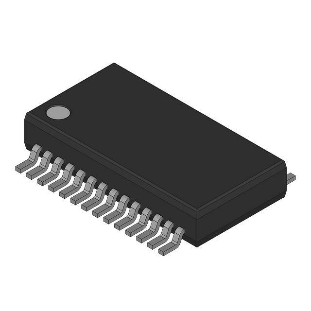
Available in 28-Lead SSOP Package
An internal differential amplifier provides true remote
sensing of the regulated supply’s positive and negative
output terminals as required by high current applications.
The RUN/SS pin provides soft-start and a defeatable,
timed, latched short-circuit shutdown to shut down both
channels. Internal foldback current limit provides protection for the external synchronous MOSFETs in the event of
an output fault. OPTI-LOOP compensation allows the
transient response to be optimized over a wide range of
output capacitance and ESR values.
U
APPLICATIO S
■
■
■
Desktop Computers
Internet/Network Servers
Large Memory Arrays
DC Power Distribution Systems
, LTC and LT are registered trademarks of Linear Technology Corporation.
OPTI-LOOP is a trademark of Linear Technology Corporation.
U
■
TYPICAL APPLICATIO
10Ω
VIN
0.1µF
TG1
BOOST1
LTC1929 SW1
RUN/SS
BG1
0.47µF
D1
L1
1µH
0.002Ω
PGND
1000pF
SENSE1 +
ITH
SENSE1 –
100pF
TG2
SGND
BOOST2
VDIFFOUT
16k
BG2
EAIN
INTVCC
–
+
VOS
VOS +
SENSE2
VOUT
1.6V/40A
0.47µF
SW2
16k
D2
+
10k
VIN
5V TO 28V
10µF
35V
CERAMIC
×4
0.1µF
L2
1µH
0.002Ω
10µF
SENSE2 –
COUT: T510E108K004AS L1, L2: CEPH149-1ROMC
+
COUT
1000µF
4V
×2
1929 F01
Figure 1. High Current 2-Phase Step-Down Converter
1
�LTC1929/LTC1929-PG
U
W W
W
ABSOLUTE
AXI U RATI GS
U
W
U
PACKAGE/ORDER I FOR ATIO
(Note 1)
ORDER PART
NUMBER
TOP VIEW
Input Supply Voltage (VIN).........................36V to – 0.3V
Topside Driver Voltages (BOOST1,2) .........42V to – 0.3V
Switch Voltage (SW1, 2) .............................36V to – 5 V
SENSE1+, SENSE2 +, SENSE1–,
SENSE2 – Voltages ........................ (1.1)INTVCC to – 0.3V
EAIN, VOS+, VOS–, EXTVCC, INTVCC,
RUN/SS, AMPMD Voltages ..........................7V to – 0.3V
Boosted Driver Voltage (BOOST-SW) ..........7V to – 0.3V
PLLFLTR, PLLIN, VDIFFOUT Voltages .... INTVCC to – 0.3V
ITH Voltage ................................................2.7V to – 0.3V
Peak Output Current 120dB open-loop gain design. The amplifier has an output slew rate of 5V/µs and is capable of
driving capacitive loads with an output RMS current typically up to 25mA. The amplifier is not capable of sinking
current and therefore must be resistively loaded to do so.
Power Good (PGOOD) Pin (LTC1929-PG Only)
The PGOOD pin is connected to an open drain of a
MOSFET. The MOSFET turns on and pulls the pin low when
the output is not within ±7.5% of its nominal output level
as determined by its resistive feedback divider. When the
output meets the ±7.5% requirement, the MOSFET is
turned off within 10µs and the pin is allowed to be pulled
up by an external source.
Short-Circuit Detection
The RUN/SS capacitor is used initially to limit the inrush
current from the input power source. Once the controllers
have been given time, as determined by the capacitor on
the RUN/SS pin, to charge up the output capacitors and
provide full load current, the RUN/SS capacitor is then
used as a short-circuit timeout circuit. If the output voltage
falls to less than 70% of its nominal output voltage the
RUN/SS capacitor begins discharging assuming that the
output is in a severe overcurrent and/or short-circuit
condition. If the condition lasts for a long enough period
as determined by the size of the RUN/SS capacitor, the
controller will be shut down until the RUN/SS pin voltage
is recycled. This built-in latchoff can be overidden by
providing a current >5µA at a compliance of 5V to the
RUN/SS pin. This current shortens the soft-start period
but also prevents net discharge of the RUN/SS capacitor
during a severe overcurrent and/or short-circuit condition. Foldback current limiting is activated when the output
voltage falls below 70% of its nominal level whether or not
the short-circuit latchoff circuit is enabled.
U
W
U
U
APPLICATIO S I FOR ATIO
The basic LTC1929 application circuit is shown in Figure␣ 1
on the first page. External component selection is driven
by the load requirement, and begins with the selection of
RSENSE1, 2. Once RSENSE1, 2 are known, L1 and L2 can be
chosen. Next, the power MOSFETs and D1 and D2 are
selected. The operating frequency and the inductor are
chosen based mainly on the amount of ripple current.
Finally, CIN is selected for its ability to handle the input
ripple current (that PolyPhaseTM operation minimizes) and
COUT is chosen with low enough ESR to meet the output
ripple voltage and load step specifications (also minimized
with PolyPhase). Current mode architecture provides inherent current sharing between output stages. The circuit
shown in Figure␣ 1 can be configured for operation up to an
input voltage of 28V (limited by the external MOSFETs).
RSENSE Selection For Output Current
RSENSE1, 2 are chosen based on the required output
current. The LTC1929 current comparator has a maximum threshold of 75mV/RSENSE and an input common
mode range of SGND to 1.1( INTVCC). The current comparator threshold sets the peak inductor current, yielding
a maximum average output current IMAX equal to the peak
value less half the peak-to-peak ripple current, ∆IL.
Allowing a margin for variations in the LTC1929 and
external component values yields:
RSENSE = 2(50mV/IMAX)
PolyPhase is a trademark of Linear Technology Corporation.
11
�LTC1929/LTC1929-PG
U
W
U
U
APPLICATIO S I FOR ATIO
When using the controller in very low dropout conditions,
the maximum output current level will be reduced due to
internal compensation required to meet stability criterion
for buck regulators operating at greater than 50% duty
factor. A curve is provided to estimate this reduction in
peak output current level depending upon the operating
duty factor.
Operating Frequency
The LTC1929 uses a constant frequency, phase-lockable
architecture with the frequency determined by an internal
capacitor. This capacitor is charged by a fixed current plus
an additional current which is proportional to the voltage
applied to the PLLFLTR pin. Refer to Phase-Locked Loop
and Frequency Synchronization in the Applications Information section for additional information.
A graph for the voltage applied to the PLLFLTR pin vs
frequency is given in Figure␣ 2. As the operating frequency
is increased the gate charge losses will be higher, reducing
efficiency (see Efficiency Considerations). The maximum
switching frequency is approximately 310kHz.
PLLFLTR PIN VOLTAGE (V)
2.5
2.0
1.5
1.0
MOSFET gate charge and transition losses. In addition to
this basic tradeoff, the effect of inductor value on ripple
current and low current operation must also be considered.
The PolyPhase approach reduces both input and output
ripple currents while optimizing individual output stages to
run at a lower fundamental frequency, enhancing efficiency.
The inductor value has a direct effect on ripple current. The
inductor ripple current ∆IL per individual section, N,
decreases with higher inductance or frequency and increases with higher VIN or VOUT:
∆IL =
VOUT VOUT
1−
fL
VIN
where f is the individual output stage operating frequency.
In a 2-phase converter, the net ripple current seen by the
output capacitor is much smaller than the individual
inductor ripple currents due to the ripple cancellation. The
details on how to calculate the net output ripple current
can be found in Application Note 77.
Figure 3 shows the net ripple current seen by the output
capacitors for the 1- and 2-phase configurations. The
output ripple current is plotted for a fixed output voltage as
the duty factor is varied between 10% and 90% on the
x-axis. The output ripple current is normalized against the
inductor ripple current at zero duty factor. The graph can
be used in place of tedious calculations, simplifying the
design process.
0.5
1.0
1-PHASE
2-PHASE
0.9
0
120
170
220
270
OPERATING FREQUENCY (kHz)
0.8
320
0.7
0.6
VO/fL
Figure 2. Operating Frequency vs VPLLFLTR
∆IO(P-P)
1929 F02
0.5
0.4
0.3
Inductor Value Calculation and Output Ripple Current
The operating frequency and inductor selection are interrelated in that higher operating frequencies allow the use
of smaller inductor and capacitor values. So why would
anyone ever choose to operate at lower frequencies with
larger components? The answer is efficiency. A higher
frequency generally results in lower efficiency because of
12
0.2
0.1
0
0.1
0.2
0.3 0.4 0.5 0.6 0.7
DUTY FACTOR (VOUT/VIN)
0.8
0.9
1929 F03
Figure 3. Normalized Output Ripple Current
vs Duty Factor [IRMS ≈ 0.3 (∆IO(P–P))]
�LTC1929/LTC1929-PG
U
W
U
U
APPLICATIO S I FOR ATIO
Accepting larger values of ∆IL allows the use of low
inductances, but can result in higher output voltage ripple.
A reasonable starting point for setting ripple current is ∆IL
= 0.4(IOUT)/2, where IOUT is the total load current. Remember, the maximum ∆IL occurs at the maximum input
voltage. The individual inductor ripple currents are determined by the inductor, input and output voltages.
EXTVCC Pin Connection). Consequently, logic-level threshold MOSFETs must be used in most applications. The only
exception is if low input voltage is expected (VIN < 5V);
then, sublogic-level threshold MOSFETs (VGS(TH) < 3V)
should be used. Pay close attention to the BVDSS specification for the MOSFETs as well; most of the logic-level
MOSFETs are limited to 30V or less.
Inductor Core Selection
Selection criteria for the power MOSFETs include the “ON”
resistance RDS(ON), reverse transfer capacitance CRSS,
input voltage, and maximum output current. When the
LTC1929 is operating in continuous mode the duty factors
for the top and bottom MOSFETs of each output stage are
given by:
Once the values for L1 and L2 are known, the type of
inductor must be selected. High efficiency converters
generally cannot afford the core loss found in low cost
powdered iron cores, forcing the use of more expensive
ferrite, molypermalloy, or Kool Mµ® cores. Actual core
loss is independent of core size for a fixed inductor value,
but it is very dependent on inductance selected. As inductance increases, core losses go down. Unfortunately,
increased inductance requires more turns of wire and
therefore copper losses will increase.
Ferrite designs have very low core loss and are preferred
at high switching frequencies, so design goals can concentrate on copper loss and preventing saturation. Ferrite
core material saturates “hard,” which means that inductance collapses abruptly when the peak design current is
exceeded. This results in an abrupt increase in inductor
ripple current and consequent output voltage ripple. Do
not allow the core to saturate!
Molypermalloy (from Magnetics, Inc.) is a very good, low
loss core material for toroids, but it is more expensive than
ferrite. A reasonable compromise from the same manufacturer is Kool Mµ. Toroids are very space efficient,
especially when you can use several layers of wire. Because they lack a bobbin, mounting is more difficult.
However, designs for surface mount are available which
do not increase the height significantly.
Power MOSFET, D1 and D2 Selection
Two external power MOSFETs must be selected for each
output stage with the LTC1929: One N-channel MOSFET
for the top (main) switch, and one N-channel MOSFET for
the bottom (synchronous) switch.
The peak-to-peak drive levels are set by the INTVCC voltage. This voltage is typically 5V during start-up (see
Main Switch Duty Cycle =
VOUT
VIN
V –V
Synchronous Switch Duty Cycle = IN OUT
VIN
The MOSFET power dissipations at maximum output
current are given by:
2
I
V
PMAIN = OUT MAX 1 + δ RDS(ON) +
VIN 2
2 I
k VIN MAX CRSS f
2
( )
( )
(
)( )
2
I
V –V
PSYNC = IN OUT MAX 1 + δ RDS(ON)
VIN
2
( )
where δ is the temperature dependency of RDS(ON) and k
is a constant inversely related to the gate drive current.
Both MOSFETs have I2R losses but the topside N-channel
equation includes an additional term for transition losses,
which peak at the highest input voltage. For VIN < 20V the
high current efficiency generally improves with larger
MOSFETs, while for VIN > 20V the transition losses rapidly
increase to the point that the use of a higher RDS(ON) device
with lower CRSS actual provides higher efficiency. The
Kool Mµ is a registered trademark of Magnetics, Inc.
13
�LTC1929/LTC1929-PG
U
W
U
U
APPLICATIO S I FOR ATIO
0.5
DC LOAD CURRENT
The term (1 + δ) is generally given for a MOSFET in the
form of a normalized RDS(ON) vs. Temperature curve, but
δ = 0.005/°C can be used as an approximation for low
voltage MOSFETs. CRSS is usually specified in the MOSFET characteristics. The constant k = 1.7 can be used to
estimate the contributions of the two terms in the main
switch dissipation equation.
0.6
RMS INPUT RIPPLE CURRNET
synchronous MOSFET losses are greatest at high input
voltage when the top switch duty factor is low or during a
short-circuit when the synchronous switch is on close to
100% of the period.
0.4
1-PHASE
2-PHASE
0.3
0.2
0.1
0
0.1
0.2
0.3 0.4 0.5 0.6 0.7
DUTY FACTOR (VOUT/VIN)
0.8
0.9
1929 F04
The Schottky diodes, D1 and D2 shown in Figure 1 conduct
during the dead-time between the conduction of the two
large power MOSFETs. This helps prevent the body diode
of the bottom MOSFET from turning on, storing charge
during the dead-time, and requiring a reverse recovery
period which would reduce efficiency. A 1A to 3A (depending on output current) Schottky diode is generally a good
compromise for both regions of operation due to the
relatively small average current. Larger diodes result in
additional transition losses due to their larger junction
capacitance.
CIN and COUT Selection
In continuous mode, the source current of each top
N-channel MOSFET is a square wave of duty cycle VOUT/
VIN. A low ESR input capacitor sized for the maximum
RMS current must be used. The details of a close form
equation can be found in Application Note 77. Figure 4
shows the input capacitor ripple current for a 2-phase
configuration with the output voltage fixed and input
voltage varied. The input ripple current is normalized
against the DC output current. The graph can be used in
place of tedious calculations. The minimum input ripple
current can be achieved when the input voltage is twice the
output voltage. The minimum is not quite zero due to
inductor ripple current.
In the graph of Figure 4, the local maximum input RMS
capacitor currents are reached when:
VOUT 2k − 1
=
VIN
4
14
where k = 1, 2.
Figure 4. Normalized RMS Input Ripple Current
vs Duty Factor for 1 and 2 Output Stages
These worst-case conditions are commonly used for design because even significant deviations do not offer much
relief. Note that capacitor manufacturer’s ripple current
ratings are often based on only 2000 hours of life. This
makes it advisable to further derate the capacitor, or to
choose a capacitor rated at a higher temperature than
required. Several capacitors may also be paralleled to meet
size or height requirements in the design. Always consult
the capacitor manufacturer if there is any question.
It is important to note that the efficiency loss is proportional to the input RMS current squared and therefore a
2-stage implementation results in 75% less power loss
when compared to a single phase design. Battery/input
protection fuse resistance (if used), PC board trace and
connector resistance losses are also reduced by the reduction of the input ripple current in a 2-phase system. The
required amount of input capacitance is further reduced by
the factor, 2, due to the effective increase in the frequency
of the current pulses.
The selection of COUT is driven by the required effective
series resistance (ESR). Typically once the ESR requirement has been met, the RMS current rating generally far
exceeds the IRIPPLE(P-P) requirements. The steady state
output ripple (∆VOUT) is determined by:
1
∆VOUT ≈ ∆IRIPPLE ESR +
16 fCOUT
�LTC1929/LTC1929-PG
U
W
U
U
APPLICATIO S I FOR ATIO
Where f = operating frequency of each stage, COUT =
output capacitance and ∆IRIPPLE = combined inductor
ripple currents.
The output ripple varies with input voltage since ∆IL is a
function of input voltage. The output ripple will be less than
50mV at max VIN with ∆IL = 0.4IOUT(MAX)/2 assuming:
COUT required ESR < 4(RSENSE) and
COUT > 1/(16f)(RSENSE)
The emergence of very low ESR capacitors in small,
surface mount packages makes very physically small
implementations possible. The ability to externally compensate the switching regulator loop using the ITH pin
(OPTI-LOOP compensation) allows a much wider selection of output capacitor types. OPTI-LOOP compensation
effectively removes constraints on output capacitor ESR.
The impedance characteristics of each capacitor type are
significantly different than an ideal capacitor and therefore
require accurate modeling or bench evaluation during
design.
Manufacturers such as Nichicon, United Chemicon and
Sanyo should be considered for high performance throughhole capacitors. The OS-CON semiconductor dielectric
capacitor available from Sanyo and the Panasonic SP
surface mount types have the lowest (ESR)(size) product
of any aluminum electrolytic at a somewhat higher price.
An additional ceramic capacitor in parallel with OS-CON
type capacitors is recommended to reduce the inductance
effects.
In surface mount applications, multiple capacitors may
have to be paralleled to meet the ESR or RMS current
handling requirements of the application. Aluminum electrolytic and dry tantalum capacitors are both available in
surface mount configurations. New special polymer surface mount capacitors offer very low ESR also but have
much lower capacitive density per unit volume. In the case
of tantalum, it is critical that the capacitors are surge tested
for use in switching power supplies. Several excellent
choices are the AVX TPS, AVX TPSV or the KEMET T510
series of surface mount tantalums, available in case heights
ranging from 2mm to 4mm. Other capacitor types include
Sanyo OS-CON, Nichicon PL series and Sprague 595D
series. Consult the manufacturer for other specific recommendations. A combination of capacitors will often result
in maximizing performance and minimizing overall cost
and size.
INTVCC Regulator
An internal P-channel low dropout regulator produces 5V
at the INTVCC pin from the VIN supply pin. The INTVCC
regulator powers the drivers and internal circuitry of the
LTC1929. The INTVCC pin regulator can supply up to 50mA
peak and must be bypassed to power ground with a
minimum of 4.7µF tantalum or electrolytic capacitor. An
additional 1µF ceramic capacitor placed very close to the
IC is recommended due to the extremely high instantaneous currents required by the MOSFET gate drivers.
High input voltage applications in which large MOSFETs
are being driven at high frequencies may cause the maximum junction temperature rating for the LTC1929 to be
exceeded. The supply current is dominated by the gate
charge supply current, in addition to the current drawn
from the differential amplifier output. The gate charge is
dependent on operating frequency as discussed in the
Efficiency Considerations section. The supply current can
either be supplied by the internal 5V regulator or via the
EXTVCC pin. When the voltage applied to the EXTVCC pin
is less than 4.7V, all of the INTVCC load current is supplied
by the internal 5V linear regulator. Power dissipation for
the IC is higher in this case by (IIN)(VIN – INTVCC) and
efficiency is lowered. The junction temperature can be
estimated by using the equations given in Note 1 of the
Electrical Characteristics. For example, the LTC1929 VIN
current is limited to less than 24mA from a 24V supply:
TJ = 70°C + (24mA)(24V)(95°C/W) = 125°C
Use of the EXTVCC pin reduces the junction temperature
to:
TJ = 70°C + (24mA)(5V)(95°C/W) = 81.4°C
The input supply current should be measured while the
controller is operating in continuous mode at maximum
VIN and the power dissipation calculated in order to prevent the maximum junction temperature from being
exceeded.
15
�LTC1929/LTC1929-PG
U
W
U
U
APPLICATIO S I FOR ATIO
EXTVCC Connection
The LTC1929 contains an internal P-channel MOSFET
switch connected between the EXTVCC and INTVCC pins.
When the voltage applied to EXTVCC rises above 4.7V, the
internal regulator is turned off and the switch closes,
connecting the EXTVCC pin to the INTVCC pin thereby
supplying internal and MOSFET gate driving power. The
switch remains closed as long as the voltage applied to
EXTVCC remains above 4.5V. This allows the MOSFET
driver and control power to be derived from the output
during normal operation (4.7V < VEXTVCC < 7V) and from
the internal regulator when the output is out of regulation
(start-up, short-circuit). Do not apply greater than 7V to
the EXTVCC pin and ensure that EXTVCC < VIN + 0.3V when
using the application circuits shown. If an external voltage
source is applied to the EXTVCC pin when the VIN supply is
not present, a diode can be placed in series with the
LTC1929’s VIN pin and a Schottky diode between the
EXTVCC and the VIN pin, to prevent current from backfeeding
VIN.
Significant efficiency gains can be realized by powering
INTVCC from the output, since the VIN current resulting
from the driver and control currents will be scaled by the
ratio: (Duty Factor)/(Efficiency). For 5V regulators this
means connecting the EXTVCC pin directly to VOUT. However, for 3.3V and other lower voltage regulators, additional circuitry is required to derive INTVCC power from the
output.
The following list summarizes the four possible connections for EXTVCC:
OPTIONAL EXTVCC CONNECTION
5V < VSEC < 7V
+
CIN
1. EXTVCC left open (or grounded). This will cause INTVCC
to be powered from the internal 5V regulator resulting in
a significant efficiency penalty at high input voltages.
2. EXTVCC connected directly to VOUT. This is the normal
connection for a 5V regulator and provides the highest
efficiency.
3. EXTVCC connected to an external supply. If an external
supply is available in the 5V to 7V range, it may be used to
power EXTVCC providing it is compatible with the MOSFET
gate drive requirements.
4. EXTVCC connected to an output-derived boost network.
For 3.3V and other low voltage regulators, efficiency gains
can still be realized by connecting EXTVCC to an outputderived voltage which has been boosted to greater than
4.7V but less than 7V. This can be done with either the
inductive boost winding as shown in Figure 5a or the
capacitive charge pump shown in Figure 5b. The charge
pump has the advantage of simple magnetics.
Topside MOSFET Driver Supply (CB,DB) (Refer to
Functional Diagram)
External bootstrap capacitors CB1 and CB2 connected to
the BOOST1 and BOOST2 pins supply the gate drive
voltages for the topside MOSFETs. Capacitor CB in the
Functional Diagram is charged though diode DB from
INTVCC when the SW pin is low. When the topside MOSFET
turns on, the driver places the CB voltage across the gatesource of the desired MOSFET. This enhances the MOSFET
and turns on the topside switch. The switch node voltage,
+
VIN
VIN
1N4148
TG1
EXTVCC
+
1µF
VOUT
T1
BAT85
N-CH
LTC1929
VN2222LL
BAT85
EXTVCC
SW1
VOUT
L1
+
+
COUT
BG1
0.22µF
RSENSE
RSENSE
SW1
BAT85
TG1
VSEC
N-CH
LTC1929
+
VIN
CIN
VIN
COUT
BG1
N-CH
N-CH
PGND
PGND
1929 F05b
1929 F05a
Figure 5a. Secondary Output Loop with EXTVCC Connection
16
Figure 5b. Capacitive Charge Pump for EXTVCC
�LTC1929/LTC1929-PG
U
W
U
U
APPLICATIO S I FOR ATIO
SW, rises to VIN and the BOOST pin rises to VIN + VINTVCC.
The value of the boost capacitor CB needs to be 30 to 100
times that of the total input capacitance of the topside
MOSFET(s). The reverse breakdown of DB must be greater
than VIN(MAX).
The final arbiter when defining the best gate drive amplitude level will be the input supply current. If a change is
made that decreases input current, the efficiency has
improved. If the input current does not change then the
efficiency has not changed either.
Output Voltage
The LTC1929 has a true remote voltage sense capability.
The sensing connections should be returned from the load
back to the differential amplifier’s inputs through a common, tightly coupled pair of PC traces. The differential
amplifier rejects common mode signals capacitively or
inductively radiated into the feedback PC traces as well as
ground loop disturbances. The differential amplifier output signal is divided down and compared with the internal
precision 0.8V voltage reference by the error amplifier.
The differential amplifier can be used in either of two
configurations according to the voltage applied to the
AMPMD pin (LTC1929 only). The first configuration, with
the connections illustrated in the Functional Diagram,
utilizes a set of internal precision resistors to enable
precision instrumentation-type measurement of the output voltage. This configuration is activated when the
AMPMD pin is tied to ground and is the default for the
LTC1929-PG. When the AMPMD pin is tied to INTVCC, the
resistors are disconnected and the amplifier inputs are
made directly available. The amplifier can then be used as
a general purpose op amp. The amplifier has a 0V to 3V
common mode input range limitation due to the internal
switching of its inputs. The output is an NPN emitter
follower without any internal pull-down current. A DC
resistive load to ground is required in order to sink current.
The output will swing from 0V to 10V (VIN ≥ VDIFFOUT + 2V).
Soft-Start/Run Function
The RUN/SS pin provides three functions: 1) Run/Shutdown, 2) soft-start and 3) a defeatable short-circuit latchoff
timer. Soft-start reduces the input power sources’ surge
currents by gradually increasing the controller’s current
limit ITH(MAX). The latchoff timer prevents very short,
extreme load transients from tripping the overcurrent
latch. A small pull-up current (>5µA) supplied to the RUN/
SS pin will prevent the overcurrent latch from operating.
The following explanation describes how the functions
operate.
An internal 1.2µA current source charges up the CSS
capacitor. When the voltage on RUN/SS reaches 1.5V, the
controller is permitted to start operating. As the voltage on
RUN/SS increases from 1.5V to 3.0V, the internal current
limit is increased from 25mV/RSENSE to 75mV/RSENSE.
The output current limit ramps up slowly, taking an
additional 1.4s/µF to reach full current. The output current
thus ramps up slowly, reducing the starting surge current
required from the input power supply. If RUN/SS has been
pulled all the way to ground there is a delay before starting
of approximately:
tDELAY =
(
)
1.5V
CSS = 1.25s / µF CSS
1.2µA
The time for the output current to ramp up is then:
tIRAMP =
(
)
3V − 1.5V
CSS = 1.25s / µF CSS
1.2µA
By pulling both RUN/SS controller pins below 0.8V the
LTC1929 is put into low current shutdown (IQ < 40µA). The
RUN/SS pins can be driven directly from logic as shown in
Figure 6. Diode D1 in Figure 6 reduces the start delay but
allows CSS to ramp up slowly providing the soft-start
function. The RUN/SS pin has an internal 6V zener clamp
(see Functional Diagram).
Fault Conditions: Overcurrent Latchoff
The RUN/SS pin also provides the ability to latch off the
controllers when an overcurrent condition is detected.
The RUN/SS capacitor, CSS, is used initially to limit the
inrush current of both controllers. After the controllers
have been started and been given adequate time to charge
up the output capacitors and provide full load current, the
RUN/SS capacitor is used for a short-circuit timer. If the
output voltage falls to less than 70% of its nominal value,
17
�LTC1929/LTC1929-PG
U
W
U
U
APPLICATIO S I FOR ATIO
after CSS reaches 4.1V, CSS begins discharging on the
assumption that the output is in an overcurrent condition.
If the condition lasts for a long enough period as determined by the size of CSS, the controller will be shut down
until the RUN/SS pin voltage is recycled. If the overload
occurs during start-up, the time can be approximated by:
If the overload occurs after start-up the voltage on the
RUN/SS capacitor will continue charging and will provide
additional time before latching off:
tLO2 ≈ (CSS • 3V)/(1.2µA) = 2.5 • 106 (CSS)
This built-in overcurrent latchoff can be overridden by
providing a pull-up resistor, RSS, to the RUN/SS pin as
shown in Figure 6. This resistance shortens the soft-start
period and prevents the discharge of the RUN/SS capacitor during a severe overcurrent and/or short-circuit condition. When deriving the 5µA current from VIN as in the
figure, current latchoff is always defeated. The diode
connecting of this pull-up resistor to INTVCC, as in
Figure␣ 6, eliminates any extra supply current during shutdown while eliminating the INTVCC loading from preventing controller start-up.
Why should you defeat current latchoff? During the
prototyping stage of a design, there may be a problem with
noise pickup or poor layout causing the protection circuit
to latch off the controller. Defeating this feature allows
troubleshooting of the circuit and PC layout. The internal
short-circuit and foldback current limiting still remains
active, thereby protecting the power supply system from
failure. A decision can be made after the design is complete whether to rely solely on foldback current limiting or
to enable the latchoff feature by removing the pull-up
resistor.
3.3V OR 5V
D1
INTVCC
RUN/SS
RSS*
Phase-Locked Loop and Frequency Synchronization
The LTC1929 has a phase-locked loop comprised of an
internal voltage controlled oscillator and phase detector.
This allows the top MOSFET turn-on to be locked to the
rising edge of an external source. The frequency range of
the voltage controlled oscillator is ±50% around the
center frequency fO. A voltage applied to the PLLFLTR pin
of 1.2V corresponds to a frequency of approximately
220kHz. The nominal operating frequency range of the
LTC1929 is 140kHz to 310kHz.
The phase detector used is an edge sensitive digital type
which provides zero degrees phase shift between the
external and internal oscillators. This type of phase detector will not lock up on input frequencies close to the
harmonics of the VCO center frequency. The PLL hold-in
range, ∆fH, is equal to the capture range, ∆fC:
∆fH = ∆fC = ±0.5 fO (150kHz-300kHz)
The output of the phase detector is a complementary pair
of current sources charging or discharging the external
filter network on the PLLFLTR pin. A simplified block
diagram is shown in Figure 7.
2.4V
RLP
10k
PHASE
DETECTOR
EXTERNAL
OSC
CLP
PLLFLTR
RSS*
D1*
CSS > (COUT )(VOUT)(10-4)(RSENSE)
The minimum recommended soft-start capacitor of CSS =
0.1µF will be sufficient for most applications.
tLO1 ≈ (CSS • 0.6V)/(1.2µA) = 5 • 105 (CSS)
VIN
The value of the soft-start capacitor CSS may need to be
scaled with output voltage, output capacitance and load
current characteristics. The minimum soft-start capacitance is given by:
PLLIN
RUN/SS
CSS
50k
DIGITAL
PHASE/
FREQUENCY
DETECTOR
OSC
CSS
*OPTIONAL TO DEFEAT OVERCURRENT LATCHOFF
Figure 6. RUN/SS Pin Interfacing
18
1929 F06
1929 F07
Figure 7. Phase-Locked Loop Block Diagram
�LTC1929/LTC1929-PG
U
W
U
U
APPLICATIO S I FOR ATIO
If the external frequency (fPLLIN) is greater than the oscillator frequency f0SC, current is sourced continuously,
pulling up the PLLFLTR pin. When the external frequency
is less than f0SC, current is sunk continuously, pulling
down the PLLFLTR pin. If the external and internal frequencies are the same but exhibit a phase difference, the
current sources turn on for an amount of time corresponding to the phase difference. Thus the voltage on the
PLLFLTR pin is adjusted until the phase and frequency of
the external and internal oscillators are identical. At this
stable operating point the phase comparator output is
open and the filter capacitor CLP holds the voltage. The
LTC1929 PLLIN pin must be driven from a low impedance
source such as a logic gate located close to the pin.
The loop filter components (CLP, RLP) smooth out the
current pulses from the phase detector and provide a
stable input to the voltage controlled oscillator. The filter
components CLP and RLP determine how fast the loop
acquires lock. Typically RLP =10kΩ and CLP is 0.01µF to
0.1µF.
Minimum On-Time Considerations
Minimum on-time tON(MIN) is the smallest time duration
that the LTC1929 is capable of turning on the top MOSFET.
It is determined by internal timing delays and the gate
charge required to turn on the top MOSFET. Low duty cycle
applications may approach this minimum on-time limit
and care should be taken to ensure that
tON(MIN) <
VOUT
()
VIN f
If the duty cycle falls below what can be accommodated by
the minimum on-time, the LTC1929 will begin to skip
cycles resulting in nonconstant frequency operation. The
output voltage will continue to be regulated, but the ripple
current and ripple voltage will increase.
The minimum on-time for the LTC1929 is generally less
than 200ns. However, as the peak sense voltage decreases
the minimum on-time gradually increases. This is of
particular concern in forced continuous applications with
low ripple current at light loads. If the duty cycle drops
below the minimum on-time limit in this situation, a
significant amount of cycle skipping can occur with correspondingly larger current and voltage ripple.
If an application can operate close to the minimum ontime limit, an inductor must be chosen that has a low
enough inductance to provide sufficient ripple amplitude
to meet the minimum on-time requirement. As a general
rule, keep the inductor ripple current of each phase equal
to or greater than 15% of IOUT(MAX) at VIN(MAX).
Efficiency Considerations
The percent efficiency of a switching regulator is equal to
the output power divided by the input power times 100%.
It is often useful to analyze individual losses to determine
what is limiting the efficiency and which change would
produce the most improvement. Percent efficiency can be
expressed as:
%Efficiency = 100% – (L1 + L2 + L3 + ...)
where L1, L2, etc. are the individual losses as a percentage
of input power.
Although all dissipative elements in the circuit produce
losses, four main sources usually account for most of the
losses in LTC1929 circuits: 1) LTC1929 VIN current (including loading on the differential amplifier output),
2) INTVCC regulator current, 3) I2R losses and 4) Topside
MOSFET transition losses.
1) The VIN current has two components: the first is the
DC supply current given in the Electrical Characteristics
table, which excludes MOSFET driver and control currents; the second is the current drawn from the differential
amplifier output. VIN current typically results in a small
(1µF) supply bypass capacitors. The
discharged bypass capacitors are effectively put in parallel
with COUT, causing a rapid drop in VOUT. No regulator can
alter its delivery of current quickly enough to prevent this
sudden step change in output voltage if the load switch
resistance is low and it is driven quickly. If the ratio of
CLOAD to COUT is greater than 1:50, the switch rise time
should be controlled so that the load rise time is limited to
approximately 25 • CLOAD. Thus a 10µF capacitor would
require a 250µs rise time, limiting the charging current to
about 200mA.
Automotive Considerations: Plugging into the
Cigarette Lighter
As battery-powered devices go mobile, there is a natural
interest in plugging into the cigarette lighter in order to
conserve or even recharge battery packs during operation.
But before you connect, be advised: you are plugging into
the supply from hell. The main battery line in an automobile is the source of a number of nasty potential transients,
including load-dump, reverse-battery, and double-battery.
Load-dump is the result of a loose battery cable. When the
cable breaks connection, the field collapse in the alternator
can cause a positive spike as high as 60V which takes
several hundred milliseconds to decay. Reverse-battery is
just what it says, while double-battery is a consequence of
tow truck operators finding that a 24V jump start cranks
cold engines faster than 12V.
The network shown in Figure 8 is the most straightforward
approach to protect a DC/DC converter from the ravages
of an automotive battery line. The series diode prevents
current from flowing during reverse-battery, while the
transient suppressor clamps the input voltage during
load-dump. Note that the transient suppressor should not
conduct during double-battery operation, but must still
clamp the input voltage below breakdown of the converter.
Although the LT1929 has a maximum input voltage of 36V,
most applications will be limited to 30V by the MOSFET
BVDSS.
50A IPK RATING
12V
TRANSIENT VOLTAGE
SUPPRESSOR
GENERAL INSTRUMENT
1.5KA24A
VIN
LTC1929
1929 F08
Figure 8. Automotive Application Protection
21
�LTC1929/LTC1929-PG
U
W
U
U
APPLICATIO S I FOR ATIO
Design Example
As a design example, assume VIN = 5V (nominal), VIN␣ =␣ 5.5V
(max), VOUT = 1.8V, IMAX = 20A, TA = 70°C and f␣ =␣ 300kHz.
The inductance value is chosen first based on a 30% ripple
current assumption. The highest value of ripple current
occurs at the maximum input voltage. Tie the FREQSET pin
to the INTVCC pin for 300kHz operation. The minimum
inductance for 30% ripple current is:
L≥
≥
VOUT VOUT
1−
VIN
f ∆I
( )
(
1.8 V
1−
300kHz 30% 10 A 5.5V
1.8 V
≥ 1.35µH
)( )( )
A 1.5µH inductor will produce 27% ripple current. The
peak inductor current will be the maximum DC value plus
one half the ripple current, or 11.4A. The minimum ontime occurs at maximum VIN:
tON(MIN) =
VOUT
1.8 V
=
= 1.1µs
VINf (5.5V )(300kHz)
The RSENSE resistors value can be calculated by using the
maximum current sense voltage specification with some
accomodation for tolerances:
50mV
RSENSE =
≈ 0.004Ω
11.4A
The power dissipation on the topside MOSFET can be
easily estimated. Using a Siliconix Si4420DY for example;
RDS(ON) = 0.013Ω, CRSS = 300pF. At maximum input
voltage with TJ (estimated) = 110°C at an elevated ambient
temperature:
PMAIN =
22
( ) [1+ (0.005)(110°C − 25°C)]
2
0.013Ω + 1.7(5.5V ) (10 A )(300pF )
(300kHz) = 0.65W
1.8 V
10
5.5V
2
The worst-case power disipated by the synchronous
MOSFET under normal operating conditions at elevated
ambient temperature and estimated 50°C junction temperature rise is:
( ) (1.48)(0.013Ω)
5.5V − 1.8 V
10 A
5.5V
= 1.29W
PSYNC =
2
A short-circuit to ground will result in a folded back current
of about:
ISC =
( ) = 6.6A
25mV
1 200ns 5.5V
+
0.004Ω 2 1.5µH
The worst-case power disipated by the synchronous
MOSFET under short-circuit conditions at elevated ambient temperature and estimated 50°C junction temperature
rise is:
( ) (1.48)(0.013Ω)
5.5V − 1.8 V
6.6 A
5.5V
= 564mW
PSYNC =
2
which is less than half of the normal, full-load dissipation.
Incidentally, since the load no longer dissipates power in
the shorted condition, total system power dissipation is
decreased by over 99%.
The duty factor for this application is:
DF =
VO 1.8 V
=
= 0.36
VIN
5V
Using Figure 4, the RMS ripple current will be:
IINRMS = (20A)(0.23) = 4.6ARMS
An input capacitor(s) with a 4.6ARMS ripple current rating
is required.
The output capacitor ripple current is calculated by using
the inductor ripple already calculated for each inductor
and multiplying by the factor obtained from Figure␣ 3
along with the calculated duty factor. The output ripple in
�LTC1929/LTC1929-PG
U
U
W
U
APPLICATIO S I FOR ATIO
continuous mode will be highest at the maximum input
voltage since the duty factor is < 50%. The maximum
output current ripple is:
( )
VOUT
0.3 at 33% D F
fL
1.8 V
0.3
∆ICOUTMAX =
300kHz 1.5µH
∆ICOUT =
(
= 1.2ARMS
)(
(
)
)
VOUTRIPPLE = 20mΩ 1.2ARMS = 24mVRMS
PC Board Layout Checklist
When laying out the printed circuit board, the following
checklist should be used to ensure proper operation of the
LTC1929. These items are also illustrated graphically in
the layout diagram of Figure␣ 11. Check the following in
your layout:
1) Are the signal and power grounds segregated? The
LTC1929 signal ground pin should return to the (–) plate
of COUT separately. The power ground returns to the
sources of the bottom N-channel MOSFETs, anodes of the
Schottky diodes, and (–) plates of CIN, which should have
as short lead lengths as possible.
2) Does the LTC1929 VOS+ pin connect to the (+) plate(s)
of COUT? Does the LTC1929 VOS– pin connect to the (–)
plate(s) of COUT? The resistive divider R1, R2 must be
connected between the VDIFFOUT and signal ground and
any feedforward capacitor across R1 should be as close as
possible to the LTC1929.
3) Are the SENSE – and SENSE + leads routed together with
minimum PC trace spacing? The filter capacitors between
SENSE + and SENSE – pin pairs should be as close as
possible to the LTC1929. Ensure accurate current sensing
with Kelvin connections.
4) Do the (+) plates of CIN connect to the drains of the
topside MOSFETs as closely as possible? This capacitor
provides the AC current to the MOSFETs. Keep the input
current path formed by the input capacitor, top and bottom
MOSFETs, and the Schottky diode on the same side of the
PC board in a tight loop to minimize conducted and
radiated EMI.
5) Is the INTVCC 1µF ceramic decoupling capacitor connected closely between INTVCC and the power ground pin?
This capacitor carries the MOSFET driver peak currents. A
small value is used to allow placement immediately adjacent to the IC.
6) Keep the switching nodes, SW1 (SW2), away from
sensitive small-signal nodes. Ideally the switch nodes
should be placed at the furthest point from the LTC1929.
7) Use a low impedance source such as a logic gate to drive
the PLLIN pin and keep the lead as short as possible.
The diagram in Figure 9 illustrates all branch currents in
a 2-phase switching regulator. It becomes very clear after
studying the current waveforms why it is critical to keep
the high-switching-current paths to a small physical size.
High electric and magnetic fields will radiate from these
“loops” just as radio stations transmit signals. The output capacitor ground should return to the negative terminal of the input capacitor and not share a common
ground path with any switched current paths. The left half
of the circuit gives rise to the “noise” generated by a
switching regulator. The ground terminations of the
synchronous MOSFETs and Schottky diodes should return to the bottom plate(s) of the input capacitor(s) with
a short isolated PC trace since very high switched currents are present. A separate isolated path from the
bottom plate(s) of the input capacitor(s) should be used
to tie in the IC power ground pin (PGND) and the signal
ground pin (SGND). This technique keeps inherent signals generated by high current pulses from taking alternate current paths that have finite impedances during the
total period of the switching regulator. External OPTILOOP compensation allows overcompensation for PC
layouts which are not optimized but this is not the
recommended design procedure.
23
�LTC1929/LTC1929-PG
U
W
U
U
APPLICATIO S I FOR ATIO
Simplified Visual Explanation of How a 2-Phase
Controller Reduces Both Input and Output RMS Ripple
Current
A multiphase power supply significantly reduces the
amount of ripple current in both the input and output
capacitors. The RMS input ripple current is divided by, and
the effective ripple frequency is multiplied up by the
number of phases used (assuming that the input voltage
is greater than the number of phases used times the output
voltage). The output ripple amplitude is also reduced by,
and the effective ripple frequency is increased by the
number of phases used. Figure 10 graphically illustrates
the principle.
The worst-case RMS ripple current for a single stage
design peaks at twice the value of the output voltage . The
worst-case RMS ripple current for a two stage design
results in peaks at 1/4 and 3/4 of input voltage. When the
RMS current is calculated, higher effective duty factor
results and the peak current levels are divided as long as
the currents in each stage are balanced. Refer to Application Note 19 for a detailed description of how to calculate
RMS current for the single stage switching regulator.
Figures 3 and 4 illustrate how the input and output
currents are reduced by using an additional phase. The
input current peaks drop in half and the frequency is
doubled for this 2-phase converter. The input capacity
requirement is thus reduced theoretically by a factor of
four! Ceramic input capacitors with their unbeatably low
ESR characteristics can be used.
24
Figure 4 illustrates the RMS input current drawn from the
input capacitance vs the duty cycle as determined by the
ratio of input and output voltage. The peak input RMS
current level of the single phase system is reduced by 50%
in a 2-phase solution due to the current splitting between
the two stages.
An interesting result of the 2-phase solution is that the VIN
which produces worst-case ripple current for the input
capacitor, VOUT = VIN/2, in the single phase design produces zero input current ripple in the 2-phase design.
The output ripple current is reduced significantly when
compared to the single phase solution using the same
inductance value because the VOUT/L discharge current
term from the stage that has its bottom MOSFET on
subtracts current from the (VIN - VOUT)/L charging current
resulting from the stage which has its top MOSFET on. The
output ripple current is:
∆IRIPPLE =
( )
2VOUT 1 − 2D 1 − D
fL 1 − 2D + 1
where D is duty factor.
The input and output ripple frequency is increased by the
number of stages used, reducing the output capacity
requirements. When VIN is approximately equal to 2(VOUT)
as illustrated in Figures 3 and 4, very low input and output
ripple currents result.
�LTC1929/LTC1929-PG
U
W
U
U
APPLICATIO S I FOR ATIO
SW1
L1
RSENSE1
D1
VIN
VOUT
RIN
CIN
+
+
COUT
RL
Figure 9. Instantaneous Current Path Flow in a Multiple Phase Switching Regulator
Figure 10. Single and 2-Phase Current Waveforms
25
�26
R2
2.7k
C11 1nF
R3
10k
R6
8.06k
C15
470pF
R5 10k
C10 100pF
C9 0.01µF
C7
0.1µF
R7
8.06k
C17
1000pF
C1 1000pF
14
13
12
11
10
9
8
7
6
5
4
3
2
1
SENSE1 –
AMPMD
15
16
17
18
19
20
21
22
23
24
25
26
27
28
C13
2.2µF
C8
0.47µF
C3, C4: OS-CON 6SP680M
C18–C21: T510E108M004
L1, L2: SUMIDA CEP149-1R0MC
Q1–Q8: FDS6670A OR FDS7760A
C12
1µF
R1
10Ω
C14
10µF
1
3
2
+
Figure 11. 5V Input, 1.6V/40A CPU Power Supply
SENSE2
+
TG2
SW2
VOS +
SENSE2 –
BOOST2
BG2
VOS –
VDIFFOUT
PGND
INTVCC
ITH
SGND
EXTVCC
BG1
PLLIN
NC
VIN
PLLFLTR
BOOST1
SW1
SENSE1 +
EAIN
NC
TG1
RUN/SS
U1
LTC1929
C2
1µF
+
R9
50Ω
C18
C16
0.47µF
D1
BAT54A
C19
+
Q7
Q5
C20
Q3
Q1
C22
1µF
R10
50Ω
+
Q8
Q6
C21
Q4
+
C4
VIN+
VIN–
5V
VOSENSE +
REMOTE SENSE
VOSENSE –
VOUT –
1.6V/40A
VOUT +
R8
0.002Ω
R4
0.002Ω
1929 F11
C24
10µF
C3
L1
1µH
L2
1µH
+
Q2
C23
1µF
LTC1929/LTC1929-PG
TYPICAL APPLICATIO S
U
�LTC1929/LTC1929-PG
U
TYPICAL APPLICATIO S
100
EFFICIENCY (%)
90
80
70
60
VIN = 5V
VOUT = 1.6V
50
0
5
10
15 20 25 30
LOAD CURRENT (A)
35
40
1929 F12
Figure 12. Efficiency Plot for Circuit of Figure 11
U
PACKAGE DESCRIPTIO
Dimensions in inches (millimeters) unless otherwise noted.
G Package
28-Lead Plastic SSOP (0.209)
(LTC DWG # 05-08-1640)
10.07 – 10.33*
(0.397 – 0.407)
28 27 26 25 24 23 22 21 20 19 18 17 16 15
7.65 – 7.90
(0.301 – 0.311)
1 2 3 4 5 6 7 8 9 10 11 12 13 14
5.20 – 5.38**
(0.205 – 0.212)
1.73 – 1.99
(0.068 – 0.078)
0° – 8°
0.13 – 0.22
(0.005 – 0.009)
0.55 – 0.95
(0.022 – 0.037)
NOTE: DIMENSIONS ARE IN MILLIMETERS
*DIMENSIONS DO NOT INCLUDE MOLD FLASH. MOLD FLASH
SHALL NOT EXCEED 0.152mm (0.006") PER SIDE
**DIMENSIONS DO NOT INCLUDE INTERLEAD FLASH. INTERLEAD
FLASH SHALL NOT EXCEED 0.254mm (0.010") PER SIDE
0.65
(0.0256)
BSC
0.25 – 0.38
(0.010 – 0.015)
Information furnished by Linear Technology Corporation is believed to be accurate and reliable.
However, no responsibility is assumed for its use. Linear Technology Corporation makes no representation that the interconnection of its circuits as described herein will not infringe on existing patent rights.
0.05 – 0.21
(0.002 – 0.008)
G28 SSOP 1098
27
�LTC1929/LTC1929-PG
28
�