LTC2389-16
16-Bit, 2.5Msps SAR ADC
with Pin-Configurable Analog
Input Range and 96dB SNR
Description
Features
2.5Msps Throughput Rate
n ±1LSB INL (Max)
n Guaranteed 16-Bit, No Missing Codes
n Pin-Configurable Analog Input Range:
±4.096V Fully Differential
0V to 4.096V Pseudo-Differential Unipolar
±2.048V Pseudo-Differential Bipolar
n 96.0dB (Fully Differential)/93.5dB (Pseudo
Differential) SNR (Typ) at fIN = 2kHz
n –116dB (Fully Differential)/–112dB (Pseudo
Differential) THD (Typ) at fIN = 2kHz
n Guaranteed Operation to 125°C
n Single 5V Supply
n Internal 20ppm/°C (Max) Reference
n Internal Reference Buffer
n 162.5mW Power Dissipation at 2.5Msps
n No Pipeline Delay, No Cycle Latency
n 1.8V to 5V I/O Voltages
n Parallel and Serial I/O Interface
n 48-pin 7mm × 7mm LQFP and QFN Packages
The LTC®2389-16 is a low noise, high speed 16-bit
successive approximation register (SAR) ADC. Operating
from a single 5V supply, the LTC2389-16 supports pinconfigurable fully differential (±4.096V), pseudo-differential unipolar (0V to 4.096V), and pseudo-differential
bipolar (±2.048V) analog input ranges, allowing it to
interface with multiple signal chain formats without requiring additional level translation or signal conditioning.
The LTC2389-16 achieves ±1LSB INL (maximum), no
missing codes at 16-bits, and 96.0dB (fully differential)/
93.5dB (pseudo differential) SNR (typical).
n
Applications
n
Medical Imaging
High Speed, Wide Dynamic Range Data Acquisition
Industrial Process Control
Instrumentation
ATE
typical application
10µF
4.096V
0V
4.096V
0V
4.096V
0V
4.096V
0V
2.048V
10Ω
+
–
49.9Ω
1nF
10Ω
1nF
49.9Ω
32k Point FFT fSMPL = 2.5Msps, fIN = 2kHz
5V 1.8V TO 5V
0.1µF
0.1µF
0
SNR = 96.0dB
–20 THD = –116dB
SINAD = 96.0dB
–40 SFDR = 117dB
10µF
PARALLEL OR 16 BIT
SERIAL INTERFACE
A0
A1
IN+
MODE0
MODE1
LTC2389-16
RESET
PD
CS
OB/2C
–
IN
PD/FD
BUSY
SAMPLE
CNVST
VCM REFOUT REFIN REFSENSE GND
CLOCK
238916 TA01a
10µF
VDD
0V
L, LT, LTC, LTM, Linear Technology and the Linear logo are registered trademarks and
SoftSpan is a trademark of Linear Technology Corporation. All other trademarks are the property
of their respective owners. Protected by U.S. Patents, including 7705765.
OVDD
1µF
AMPLITUDE (dBFS)
n
n
n
n
The LTC2389-16 includes a precision internal 4.096V
reference, with a guaranteed 0.5% initial accuracy and a
±20ppm/°C (maximum) temperature coefficient, as well
as an internal reference buffer. Fast 2.5Msps throughput
with no cycle latency in the parallel interface modes
makes the LTC2389-16 ideally suited for a wide variety
of high speed applications. An internal oscillator sets
the conversion time, easing external timing considerations. The LTC2389-16 dissipates only 162.5mW at
2.5Msps, while both nap and sleep power-down modes
are provided to further reduce power consumption during
inactive periods.
–60
–80
–100
–120
–140
–160
–180
0
250
500
750
FREQUENCY (kHz)
1000
1250
238916 TA01b
238916f
1
�LTC2389-16
Absolute Maximum Ratings (Notes 1, 2)
Supply Voltage (VDD , OVDD)........................................6V
Analog Input Voltage (Note 3)
IN+, IN–, REFIN, CNVST......(GND – 0.3V) to (VDD + 0.3V)
Digital Input Voltage
(Note 3)........................... (GND – 0.3V) to (OVDD + 0.3V)
Digital Output Voltage
(Note 3)........................... (GND – 0.3V) to (OVDD + 0.3V)
Power Dissipation............................................... 500mW
Operating Temperature Range
LTC2389C................................................. 0°C to 70°C
LTC2389I..............................................–40°C to 85°C
LTC2389H........................................... –40°C to 125°C
Storage Temperature Range................... –65°C to 150°C
Lead Temperature (Soldering, 10 sec)
LX Package........................................................ 300°C
Pin Configuration
GND
VDD
VDD
VDD
GND
IN+
IN–
GND
VDD
REFSENSE
REFIN
REFOUT
TOP VIEW
GND 1
VDD 2
VDD 3
MODE0 4
MODE1 5
OB/2C 6
A0 7
A1 8
D0 9
D1 10
D2 11
D3 12
48
47
46
45
44
43
42
41
40
39
38
37
48
47
46
45
44
43
42
41
40
39
38
37
GND
VDD
VDD
VDD
GND
IN+
IN–
GND
VDD
REFSENSE
REFIN
REFOUT
TOP VIEW
VCM
GND
CNVST
PD
RESET
CS
PD/FD
BUSY
D15
D14
D13
D12
GND 1
VDD 2
VDD 3
MODE0 4
MODE1 5
OB/2C 6
A0 7
A1 8
D0 9
D1 10
D2 11
D3 12
36
35
34
33
32
31
30
29
28
27
26
25
49
GND
VCM
GND
CNVST
PD
RESET
CS
PD/FD
BUSY
D15
D14
D13
D12
D4 13
D5 14
D6 15
D7 16
GND 17
OVDD 18
VDD 19
GND 20
D8 21
D9/SDI 22
D10/SDO 23
D11/SCK 24
D4 13
D5 14
D6 15
D7 16
GND 17
OVDD 18
VDD 19
GND 20
D8 21
D9/SDI 22
D10/SDO 23
D11/SCK 24
36
35
34
33
32
31
30
29
28
27
26
25
UK PACKAGE
48-LEAD (7mm × 7mm) PLASTIC QFN
LX PACKAGE
48-LEAD (7mm × 7mm) PLASTIC LQFP
TJMAX = 125°C, θJA = 29°C/W
EXPOSED PAD (PIN 49) IS GND, MUST BE SOLDERED TO PCB
TJMAX = 150°C, θJA = 50°C/W
Order Information
LEAD FREE FINISH
TAPE AND REEL
PART MARKING*
PACKAGE DESCRIPTION
TEMPERATURE RANGE
LTC2389CUK-16#PBF
LTC2389CUK-16#TRPBF
LTC2389UK-16
48-Lead 7mm × 7mm Plastic QFN
0°C to 70°C
LTC2389IUK-16#PBF
LTC2389IUK-16#TRPBF
LTC2389UK-16
48-Lead 7mm × 7mm Plastic QFN
–40°C to 85°C
LEAD FREE FINISH
TRAY
PART MARKING*
PACKAGE DESCRIPTION
TEMPERATURE RANGE
LTC2389CLX-16#PBF
LTC2389CLX-16#PBF
LTC2389LX-16
48-Lead 7mm × 7mm Plastic LQFP
0°C to 70°C
LTC2389ILX-16#PBF
LTC2389ILX-16#PBF
LTC2389LX-16
48-Lead 7mm × 7mm Plastic LQFP
–40°C to 85°C
LTC2389HLX-16#PBF
LTC2389HLX-16#PBF
LTC2389LX-16
48-Lead 7mm × 7mm Plastic LQFP
–40°C to 125°C
Consult LTC Marketing for parts specified with wider operating temperature ranges. *The temperature grade is identified by a label on the shipping container.
Consult LTC Marketing for information on non-standard lead based finish parts.
For more information on lead free part marking, go to: http://www.linear.com/leadfree/
For more information on tape and reel specifications, go to: http://www.linear.com/tapeandreel/
238916f
2
�LTC2389-16
Analog
Input The l denotes the specifications which apply over the full operating temperature range, otherwise
specifications are at TA = 25°C. (Note 4)
SYMBOL
PARAMETER
CONDITIONS
VIN+
Absolute Input Range (IN+)
MIN
TYP
(Note 5)
l
–0.1
VREF + 0.1
V
VIN–
Absolute Input Range (IN–)
Fully Differential (Note 5)
Pseudo-Differential Unipolar (Note 5)
Pseudo-Differential Bipolar (Note 5)
l
l
l
–0.1
–0.1
VREF /2 – 0.1
VREF + 0.1
0.1
VREF /2 + 0.1
V
V
V
VIN+ – VIN–
Input Differential Voltage Range
Fully Differential
Pseudo-Differential Unipolar
Pseudo-Differential Bipolar
l
l
l
–VREF
0
–VREF /2
VREF
VREF
VREF /2
V
V
V
VCM
Input Common Mode Voltage Range
Fully Differential
l
VREF /2 – 0.1
IIN
Analog Input Leakage Current
C- and I-Grades
H-Grade
l
l
–1
–2
CIN
Analog Input Capacitance
Sample Mode
Hold Mode
CMRR
Input Common Mode Rejection Ratio
VIHCNVST
CNVST High Level Input Voltage
VILCNVST
CNVST Low Level Input Voltage
IINCNVST
CNVST Input Current
0
VREF /2
VREF /2
UNITS
VREF /2 + 0.1
V
1
2
µA
µA
45
5
pF
pF
70
dB
1.5
l
V
l
VIN = 0V to VDD
MAX
–25
l
0.5
V
–60
µA
Converter
Characteristics The l denotes the specifications which apply over the full operating
temperature range, otherwise specifications are at TA = 25°C. (Note 4)
SYMBOL
PARAMETER
CONDITIONS
MIN
TYP
MAX
UNITS
Resolution
l
16
Bits
No Missing Codes
l
16
Bits
Transition Noise
Fully Differential
Pseudo-Differential Unipolar
Pseudo-Differential Bipolar
0.19
0.38
0.38
INL
Integral Linearity Error
Fully Differential (Note 6)
Pseudo-Differential Unipolar (Note 6)
Pseudo-Differential Bipolar (Note 6)
l
l
l
–1
–1
–1
±0.3
±0.3
±0.3
1
1
1
LSB
LSB
LSB
DNL
Differential Linearity Error
Fully Differential
Pseudo-Differential Unipolar
Pseudo-Differential Bipolar
l
l
l
–0.6
–0.7
–0.7
±0.1
±0.1
±0.1
0.6
0.7
0.7
LSB
LSB
LSB
ZSE
Zero-Scale Error
Fully Differential (Note 7)
Pseudo-Differential Unipolar (Note 7)
Pseudo-Differential Bipolar (Note 7)
l
l
l
–3
–4
–4
0
0
0
3
4
4
LSB
LSB
LSB
External Reference (Note 7)
Internal Reference (Note 7)
l
Zero-Scale Error Drift
FSE
Full-Scale Error
Full-Scale Error Drift
LSBRMS
LSBRMS
LSBRMS
±0.05
ppm/°C
0.15
0.15
±5
%
%
ppm/°C
238916f
3
�LTC2389-16
Dynamic
Accuracy The l denotes the specifications which apply over the full operating temperature range,
otherwise specifications are at TA = 25°C. AIN = –1dBFS (Notes 4, 8)
SYMBOL
PARAMETER
CONDITIONS
SINAD
Signal-to-(Noise +
Distortion) Ratio
Fully Differential, fIN = 2kHz
Pseudo-Differential Unipolar, fIN = 2kHz
Pseudo-Differential Bipolar, fIN = 2kHz
SNR
THD
SFDR
MIN
TYP
l
l
l
94.4
91.2
91.7
96.0
93.2
93.5
dB
dB
dB
Fully Differential, fIN = 2kHz (H-Grade)
Pseudo-Differential Unipolar, fIN = 2kHz (H-Grade)
Pseudo-Differential Bipolar, fIN = 2kHz (H-Grade)
l
l
l
94.3
91.0
91.5
96.0
93.2
93.5
dB
dB
dB
Fully Differential, fIN = 2kHz
Pseudo-Differential Unipolar, fIN = 2kHz
Pseudo-Differential Bipolar, fIN = 2kHz
l
l
l
95.1
91.7
92.1
96.0
93.2
93.5
dB
dB
dB
Fully Differential, fIN = 2kHz (H-Grade)
Pseudo-Differential Unipolar, fIN = 2kHz (H-Grade)
Pseudo-Differential Bipolar, fIN = 2kHz (H-Grade)
l
l
l
94.9
91.5
91.9
96.0
93.2
93.5
dB
dB
dB
Fully Differential, fIN = 2kHz, First 5 Harmonics
Pseudo-Differential Unipolar, fIN = 2kHz, First 5 Harmonics
Pseudo-Differential Bipolar, fIN = 2kHz, First 5 Harmonics
l
l
l
–116
–112
–111
–103
–101
–102
dB
dB
dB
Fully Differential, fIN = 2kHz, First 5 Harmonics (H-Grade)
Pseudo-Differential Unipolar, fIN = 2kHz, First 5 Harmonics (H-Grade)
Pseudo-Differential Bipolar, fIN = 2kHz, First 5 Harmonics (H-Grade)
l
l
l
–116
–112
–111
–103
–101
–102
dB
dB
dB
Fully Differential, fIN = 2kHz
Pseudo-Differential Unipolar, fIN = 2kHz
Pseudo-Differential Bipolar, fIN = 2kHz
l
l
l
104
102
102
117
113
112
dB
dB
dB
Fully Differential, fIN = 2kHz (H-Grade)
Pseudo-Differential Unipolar, fIN = 2kHz (H-Grade)
Pseudo-Differential Bipolar, fIN = 2kHz (H-Grade)
l
l
l
103
102
102
117
113
112
dB
dB
dB
–3dB Input Bandwidth
50
MHz
Aperture Delay
0.5
ns
Signal-to-Noise Ratio
Total Harmonic
Distortion
Spurious-Free
Dynamic Range
Aperture Jitter
Transient Response
Full-Scale Step
MAX
UNITS
1
psRMS
70
ns
Reference
Characteristics
The l denotes the specifications which apply over the full operating
temperature range, otherwise specifications are at TA = 25°C. (Note 4)
SYMBOL
PARAMETER
CONDITIONS
MIN
TYP
MAX
UNITS
VREFOUT
Internal Reference Voltage
REFOUT Tied to REFIN, IOUT = 0µA
4.076
4.096
4.116
V
VREFOUT Tempco
IOUT = 0µA (Note 9)
±10
±20
REFOUT Output Impedance
–0.1mA ≤ IOUT ≤ 0.1mA
2.3
kΩ
REFOUT Line Regulation
VDD = 4.75V to 5.25V
0.3
mV/V
VREF
Converter REFIN Voltage
4.076
REFIN Input Impedance
VCM Output Voltage
l
4.096
74
IOUT = 0µA
2.08
4.116
ppm/°C
V
kΩ
V
238916f
4
�LTC2389-16
Digital
Inputs And Digital Outputs The l denotes the specifications which apply over the full
operating temperature range, otherwise specifications are at TA = 25°C. (Note 4)
SYMBOL
PARAMETER
VIH
High Level Input Voltage
CONDITIONS
l
VIL
Low Level Input Voltage
l
IIN
Digital Input Current
CIN
Digital Input Capacitance
VOH
High Level Output Voltage
IOUT = –500µA
l
VOL
Low Level Output Voltage
IOUT = 500µA
l
IOZ
Hi-Z Output Leakage Current
VOUT = 0V to OVDD
l
ISOURCE
Output Source Current
VOUT = 0V
–10
mA
ISINK
Output Sink Current
VOUT = OVDD
10
mA
VIN = 0V to OVDD
MIN
TYP
MAX
UNITS
0.8 • OVDD
V
–10
l
0.2 • OVDD
V
10
µA
5
pF
OVDD – 0.2
V
–10
0.2
V
10
µA
Power
Requirements The l denotes the specifications which apply over the full operating temperature
range, otherwise specifications are at TA = 25°C. (Note 4)
SYMBOL
PARAMETER
MIN
TYP
MAX
UNITS
VDD
Supply Voltage
CONDITIONS
l
4.75
5
5.25
V
OVDD
Supply Voltage
l
1.71
5.25
V
IVDD
Core Supply Current
2.5Msps Sample Rate
2.5Msps Sample Rate, Internal Reference Enabled
IOVDD
I/O Supply Current
2.5Msps Sample Rate (CL = 15pF)
IPD
Power Down Current
(IVDD + IOVDD)
Conversion Done, PD = OVDD , Other Digital Inputs
Tied to OVDD or GND
PD
Power Dissipation
2.5Msps Sample Rate
Conversion Done, PD = OVDD , Other Digital Inputs
Tied to OVDD or GND
32.5
34.1
l
36
mA
mA
1.6
l
mA
15
250
µA
162.5
75
180
1250
mW
µW
Timing
Characteristics
The l denotes the specifications which apply over the full operating temperature
range, otherwise specifications are at TA = 25°C. (Note 4)
SYMBOL
PARAMETER
CONDITIONS
fSMPL
Sampling Frequency
Parallel Output Modes
Serial Output Mode
tCONV
Conversion Time
tACQ
Acquisition Time
tACQ = tCYC – tCONV – tBUSYLH (Note 10)
MIN
TYP
l
l
l
245
280
l
77
110
MAX
UNITS
2.5
2.0
Msps
Msps
310
ns
ns
tCYC
Time Between CNVST↓
l
400
ns
tCNVSTL
CNVST Low Time
l
20
ns
tCNVSTH
CNVST High Time
l
200
ns
tBUSYLH
CNVST↓ to BUSY Delay
tRESETH
RESET Pulse Width
tSCK
SCK Period
tSCKH
SCK High Time
tSCKL
CL = 15pF
13
l
ns
l
200
ns
l
10
ns
l
4
ns
SCK Low Time
l
4
ns
tDSCK
SCK↓ Delay From CS↓
l
10
ns
tSSDI
SDI Setup Time From SCK↓
l
2
ns
(Notes 5, 11)
238916f
5
�LTC2389-16
Timing
Characteristics
The l denotes the specifications which apply over the full operating temperature
range, otherwise specifications are at TA = 25°C. (Note 4)
tHSDI
SDI Hold Time From SCK↓
tDSDO
SDO Data Valid Delay From SCK↑
CL = 15pF
l
tHSDO
SDO Data Remains Valid Delay From SCK↑
CL = 15pF
l
1
tDDBUSYL
Data Valid to BUSY↓
CL = 15pF
l
1
tEN
Bus Enable Time After CS↓
tDDA1
Data Valid Delay From A1 Transition
tDIS
Bus Relinquish Time After CS↑
l
CL = 15pF
Note 1: Stresses beyond those listed under Absolute Maximum Ratings
may cause permanent damage to the device. Exposure to any Absolute
Maximum Rating condition for extended periods may affect device
reliability and lifetime.
Note 2: All voltage values are with respect to ground.
Note 3: When these pin voltages are taken below ground or above
VDD or OVDD, they will be clamped by internal diodes. This product can
handle input currents up to 100mA below ground, or above VDD or OVDD,
without latchup.
Note 4: VDD = 5V, OVDD = 5V, VREF = 4.096V external reference,
fSMPL = 2.5MHz, unless otherwise noted.
Note 5: Recommended operating conditions.
Note 6: Integral nonlinearity is defined as the deviation of a code from a
straight line passing through the actual endpoints of the transfer curve.
The deviation is measured from the center of the quantization band.
Note 7: Fully differential zero-scale error is the offset voltage measured
from –0.5LSB when the output code flickers between 0000 0000 0000
0000 and 1111 1111 1111 1111 in two’s complement format. Unipolar
1
ns
9
ns
ns
ns
l
11
ns
l
8
ns
l
11
ns
zero-scale error is the offset voltage measured from 0.5LSB when the
output code flickers between 0000 0000 0000 0000 and 0000 0000
0000 0001. Bipolar zero-scale error is the offset voltage measured from
–0.5LSB when the output code flickers between 0000 0000 0000 0000 and
1111 1111 1111 1111. Fully differential full-scale error is the worst-case
deviation of the first and last code transitions from ideal and includes the
effect of offset error. Unipolar full-scale error is the deviation of the last
code transition from ideal and includes the effect of offset error. Bipolar
full-scale error is the worst-case deviation of the first and last code
transitions from ideal and includes the effect of offset error.
Note 8: All specifications in dB are referred to a full-scale ±4.096V (fully
differential), 0V to 4.096V (pseudo-differential unipolar), or ±2.048V
(pseudo-differential bipolar) input with a 4.096V reference voltage.
Note 9: Temperature coefficient is calculated by dividing the maximum
change in output voltage by the specified temperature range.
Note 10: Guaranteed by design, not subject to test.
Note 11: A tSCK period of 10ns minimum allows a shift clock frequency of
up to 100MHz for rising capture.
0.8 • OVDD
tWIDTH
0.2 • OVDD
tDELAY
tDELAY
0.8 • OVDD
0.8 • OVDD
0.2 • OVDD
0.2 • OVDD
50%
50%
238916 F01
Figure 1. Voltage Levels for Timing Specifications
238916f
6
�LTC2389-16
Typical Performance Characteristics
TA = 25°C, VDD = 5V, OVDD = 2.5V, VREF = 4.096V
External Reference, Fully Differential Range (PD/FD = 0V), VCM = 2.048V, fSMPL = 2.5Msps, unless otherwise noted.
0.5
INTERNAL REF
EXTERNAL REF
0.4
0.2
0.2
0
–0.2
–0.4
–0.2
–0.4
49152
OUTPUT CODE
–0.5
65536
40000
0
16384
238916 G01
240000
4.096
REFERENCE OUTPUT (V)
4.097
200000
COUNTS
160000
120000
80000
40000
32768
49152
0
65536
0
32762
32763
32764
CODE
32765
32766
4.095
4.094
4.093
4.092
4.091
–90
SNR
94
93
SINAD
92
91
90
89
0
12.5 25 37.5 50 62.5 75 87.5 100
FREQUENCY (kHz)
238916 G07
–100
–120
0
250
500
1000
1250
238916 G06
SNR, SINAD vs Input Level,
fIN = 2kHz
SNR
96.5
–100
–105
–110
THD
–115
3RD
–120
–130
750
FREQUENCY (kHz)
97.0
96.0
SINAD
95.5
2ND
–125
88
–80
–180
5 25 45 65 85 105 125
TEMPERATURE (°C)
–95
THD, HARMONICS (dB)
95
–60
THD, Harmonics vs Input Frequency
96
238916 G03
32k Point FFT fSMPL = 2.5Msps,
fIN = 2kHz
238916 G05
–85
2
–160
238916 G04
97
1
–140
4.089
–55 –35 –15
SNR, SINAD vs Input Frequency
0
CODE
–1
SNR = 96.0dB
–20 THD = –116dB
SINAD = 96.0dB
–40 SFDR = 117dB
TC = 8ppm/°C
4.090
0
–2
238916 G02
Internal Reference Output
vs Temperature
280000
SNR, SINAD (dB)
80000
OUTPUT CODE
DC Histogram (Near Full-Scale)
87
120000
–0.1
–0.8
32768
160000
0
–0.3
16384
200000
0.1
–0.6
0
240000
COUNTS
DNL ERROR (LSB)
0.3
–1.0
INTERNAL REF
EXTERNAL REF
0.4
0.6
DC Histogram (Zero-Scale)
280000
AMPLITUDE (dBFS)
0.8
INL ERROR (LSB)
Differential Nonlinearity
vs Output Code
SNR, SINAD (dB)
1.0
Integral Nonlinearity
vs Output Code
0
12.5 25 37.5 50 62.5 75 87.5 100
FREQUENCY (kHz)
238916 G08
95.0
–40
–30
–10
–20
INPUT LEVEL (dB)
0
238916 G09
238916f
7
�LTC2389-16
Typical Performance Characteristics
TA = 25°C, VDD = 5V, OVDD = 2.5V, VREF = 4.096V
External Reference, Fully Differential Range (PD/FD = 0V), VCM = 2.048V, fSMPL = 2.5Msps, unless otherwise noted.
THD, Harmonics vs Temperature,
fIN = 2kHz
–110
97
–115
96
SINAD
SNR
95
INL/DNL vs Temperature
1.0
THD
INL/ DNL ERROR (LSB)
98
THD, HARMONICS (dB)
SNR, SINAD (dB)
SNR, SINAD vs Temperature,
fIN = 2kHz
3RD
–120
–125
2ND
–130
94
93
–55 –35 –15
–135
–55 –35 –15
5 25 45 65 85 105 125
TEMPERATURE (°C)
Offset Error vs Temperature
+FS
10
5
0
–5
–FS
–10
–15
–25
–55 –35 –15
15
10
0
–55 –35 –15
5 25 45 65 85 105 125
TEMPERATURE (°C)
80
30
40
30
20
75
25
70
20
CMRR (dB)
SUPPLY CURRENT (mA)
50
IVDD
15
5 25 45 65 85 105 125
TEMPERATURE (°C)
238916 G16
0
65
60
10
55
5
10
5 25 45 65 85 105 125
TEMPERATURE (°C)
CMRR vs Input Frequency
35
IVDD + IOVDD
IOVDD
238916 G15
Supply Current
vs Sampling Frequency
70
POWER-DOWN CURRENT (µA)
20
238916 G14
Power-Down Current
vs Temperature
0
–55 –35 –15
25
5
238916 G13
60
IVDD
30
15
–20
5 25 45 65 85 105 125
TEMPERATURE (°C)
5 25 45 65 85 105 125
TEMPERATURE (°C)
Supply Current vs Temperature
35
SUPPLY CURRENT (mA)
FULL-SCALE ERROR (LSB)
OFFSET ERROR (LSB)
–0.5
MIN INL
–0.5
238916 G12
25
0
MIN DNL
–1.0
–55 –35 –15
5 25 45 65 85 105 125
TEMPERATURE (°C)
20
80
MAX DNL
0
Full-Scale Error vs Temperature
1.0
0.5
MAX INL
238916 G11
238916 G10
–1.0
–55 –35 –15
0.5
IOVDD
1
10
100
1000
SAMPLING FREQUENCY (kHz)
10000
238916 G17
50
0
250
500
750
FREQUENCY (kHz)
1000
1250
238916 G18
238916f
8
�LTC2389-16
Typical Performance Characteristics
TA = 25°C, VDD = 5V, OVDD = 2.5V, VREF = 4.096V
External Reference, Pseudo-Differential Unipolar Range (PD/FD = OVDD, OB/2C = OVDD), fSMPL = 2.5Msps, unless otherwise noted.
Differential Nonlinearity
vs Output Code
Integral Nonlinearity vs Output Code
INTERNAL REF
EXTERNAL REF
0.8
0.6
0.3
0.4
0.2
0.2
0
–0.2
–0.4
49152
OUTPUT CODE
–0.5
65536
80000
–0.2
–0.3
32768
120000
0
–0.4
16384
160000
–0.1
–0.8
0
200000
0.1
–0.6
40000
0
16384
238916 G19
32768
49152
OUTPUT CODE
0
65536
32k Point FFT fSMPL = 2.5Msps,
fIN = 2kHz
DC Histogram (Near Full-Scale)
240000
AMPLITUDE (dBFS)
COUNTS
120000
80000
40000
0
65530
65531
65532
CODE
65533
92
–80
–100
–120
82
750
1000
FREQUENCY (kHz)
238916 G22
THD, Harmonics vs Input Frequency
–75
94.0
80
1250
238916 G23
SNR, SINAD vs Input Level,
fIN = 2kHz
95
–80
0
12.5 25 37.5 50 62.5 75 87.5 100
FREQUENCY (kHz)
238916 G24
SNR, SINAD vs Temperature,
fIN = 2kHz
SNR
–85
2ND
–105
3RD
–110
–115
93.0
SNR, SINAD (dB)
THD
–95
–100
94
SNR
93.5
–90
SNR, SINAD (dB)
THD, HARMONICS (dB)
SINAD
86
–160
500
SNR
88
84
250
6
238916 G21
90
–140
0
5
94
–60
–180
65534
4
CODE
SNR, SINAD vs Input Frequency
SNR = 93.2dB
–20 THD = –112dB
SINAD = 93.2dB
–40 SFDR = 113dB
160000
3
96
0
200000
2
238916 G20
SNR, SINAD (dB)
–1.0
DC Histogram (Near Zero-Scale)
240000
INTERNAL REF
EXTERNAL REF
0.4
DNL ERROR (LSB)
INL ERROR (LSB)
0.5
COUNTS
1.0
SINAD
92.5
93 SINAD
92
91
–120
–125
–130
0
12.5 25 37.5 50 62.5 75 87.5 100
FREQUENCY (kHz)
238916 G25
92.0
–40
–30
–10
–20
INPUT LEVEL (dB)
0
238916 G26
90
–55 –35 –15
5 25 45 65 85 105 125
TEMPERATURE (°C)
238916 G27
238916f
9
�LTC2389-16
Typical Performance Characteristics
TA = 25°C, VDD = 5V, OVDD = 2.5V, VREF = 4.096V
External Reference, Pseudo-Differential Unipolar Range (PD/FD = OVDD, OB/2C = OVDD), fSMPL = 2.5Msps, unless otherwise noted.
–115
Offset Error vs Temperature
1.0
THD
2ND
–120
–125
3RD
0.5
MAX INL
OFFSET ERROR (LSB)
THD, HARMONICS (dB)
–110
INL/DNL vs Temperature
1.0
INL/ DNL ERROR (LSB)
–105
THD, Harmonics vs Temperature,
fIN = 2kHz
MAX DNL
0
MIN DNL
MIN INL
–0.5
0.5
0
–0.5
–130
–135
–55 –35 –15
5 25 45 65 85 105 125
TEMPERATURE (°C)
–1.0
–55 –35 –15
5 25 45 65 85 105 125
TEMPERATURE (°C)
238916 G29
238916 G28
5 25 45 65 85 105 125
TEMPERATURE (°C)
238916 G30
CMRR vs Input Frequency
80
75
70
CMRR (dB)
FULL-SCALE ERROR (LSB)
Full-Scale Error vs Temperature
35
30
25
20
15
10
5
0
–5
–10
–15
–20
–25
–30
–35
–55 –35 –15
–1.0
–55 –35 –15
65
60
55
5 25 45 65 85 105 125
TEMPERATURE (°C)
238916 G31
50
0
250
500
750
FREQUENCY (kHz)
1000
1250
238916 G32
238916f
10
�LTC2389-16
Typical Performance Characteristics
TA = 25°C, VDD = 5V, OVDD = 2.5V, VREF = 4.096V
External Reference, Pseudo-Differential Bipolar Range (PD/FD = OVDD, OB/2C = OV), fSMPL = 2.5Msps, unless otherwise noted.
Integral Nonlinearity
vs Output Code
INTERNAL REF
EXTERNAL REF
0.8
0.6
0.3
0.4
0.2
0.2
0
–0.2
–0.4
49152
OUTPUT CODE
–0.5
65536
40000
0
16384
32768
49152
OUTPUT CODE
238916 G33
0
65536
240000
80000
40000
0
32762
32763
32764
CODE
32765
–80
–100
–120
88
86
84
–160
82
250
500
750
1000
FREQUENCY (kHz)
238916 G36
THD, Harmonics vs Input Frequency
94.5
80
1250
238916 G37
SNR, SINAD vs Input Level,
fIN = 2kHz
95
–80
–95
–100
3RD
–105
–110
–115
SNR
93.5
SINAD
93.0
–120
0
12.5 25 37.5 50 62.5 75 87.5 100
FREQUENCY (kHz)
238916 G38
SNR, SINAD vs Temperature,
fIN = 2kHz
SNR
94
94.0
2ND
SNR, SINAD (dB)
THD
–90
SNR, SINAD (dB)
THD, HARMONICS (dB)
–85
SINAD
90
–140
0
2
238916 G35
SNR
92
–60
–180
32766
1
94
SNR, SINAD (dB)
AMPLITUDE (dBFS)
COUNTS
120000
0
CODE
96
SNR = 93.5dB
–20 THD = –111dB
SINAD = 93.5dB
–40 SFDR = 112dB
160000
–1
SNR, SINAD vs Input Frequency
0
200000
–2
238916 G34
32k Point FFT fSMPL = 2.5Msps,
fIN = 2kHz
DC Histogram (Near Full-Scale)
–75
80000
–0.2
–0.4
32768
120000
–0.1
–0.8
16384
160000
0
–0.3
0
200000
0.1
–0.6
–1.0
DC Histogram (Zero-Scale)
240000
INTERNAL REF
EXTERNAL REF
0.4
DNL ERROR (LSB)
INL ERROR (LSB)
0.5
COUNTS
1.0
Differential Nonlinearity
vs Output Code
SINAD
93
92
91
–125
–130
0
12.5 25 37.5 50 62.5 75 87.5 100
FREQUENCY (kHz)
238916 G39
92.5
–40
–30
–10
–20
INPUT LEVEL (dB)
0
238916 G40
90
–55 –35 –15
5 25 45 65 85 105 125
TEMPERATURE (°C)
238916 G41
238916f
11
�LTC2389-16
Typical Performance Characteristics
TA = 25°C, VDD = 5V, OVDD = 2.5V, VREF = 4.096V
External Reference, Pseudo-Differential Bipolar Range (PD/FD = OVDD, OB/2C = OV), fSMPL = 2.5Msps, unless otherwise noted.
2ND
–120
–125
–130
–135
–55 –35 –15
0.5
MAX INL
OFFSET ERROR (LSB)
THD, HARMONICS (dB)
Offset Error vs Temperature
1.0
THD
–110
–115
INL/DNL vs Temperature
1.0
INL/ DNL ERROR (LSB)
–105
THD, Harmonics vs Temperature,
fIN = 2kHz
MAX DNL
0
MIN DNL
MIN INL
–0.5
0.5
0
–0.5
3RD
5 25 45 65 85 105 125
TEMPERATURE (°C)
–1.0
–55 –35 –15
238916 G42
–1.0
–55 –35 –15
5 25 45 65 85 105 125
TEMPERATURE (°C)
5 25 45 65 85 105 125
TEMPERATURE (°C)
238916 G44
238916 G43
CMRR vs Input Frequency
Full-Scale Error vs Temperature
25
80
15
75
+FS
10
70
5
0
–5
–FS
–10
–15
CMRR (dB)
FULL-SCALE ERROR (LSB)
20
65
60
55
–20
–25
–55 –35 –15
5 25 45 65 85 105 125
TEMPERATURE (°C)
238916 G45
50
0
250
500
750
FREQUENCY (kHz)
1000
1250
238916 G46
238916f
12
�LTC2389-16
Pin Functions
GND (Pins 1, 17, 20, 35, 41, 44, 48, Exposed Pad
Pin 49 (QFN Only)): Ground. Solder all GND pins and
exposed pad to the ground plane.
VDD (Pins 2, 3, 19, 40, 45, 46, 47): 5V Power Supply.
The range of VDD is 4.75V to 5.25V. Bypass VDD network
to GND with a 0.1μF ceramic capacitor close to each pin
and a 10μF ceramic capacitor in parallel.
MODE0 (Pin 4): Data Bus Configuration Input. This pin,
in conjunction with Pin 8 (A1), controls the parsing and
presentation of conversion results on the output data bus.
Based on the state of MODE0, the bus is configured to
provide either 16-bit/8-bit parallel (MODE0 = 0), or serial
(MODE0 = 1) data, as described in Table 1. Digital outputs
that are not active in a particular mode become Hi-Z. Logic
levels are determined by OVDD. For information regarding
pin compatibility with 18-bit versions of the LTC2389 family,
refer to the Pin Compatibility with LTC2389-18 section.
MODE1 (Pin 5): Data Bus Configuration Input. This pin is
reserved for use in 18-bit versions of the LTC2389 family,
and for 16-bit versions of the family it should be driven to
a logic low level. Logic levels are determined by OVDD. For
information regarding pin compatibility with 18-bit versions
of the LTC2389 family, refer to the Pin Compatibility with
LTC2389-18 section.
OB/2C (Pin 6): Offset Binary/ Two’s Complement Input.
This pin, in conjunction with Pin 30 (PD/FD), controls the
analog input range of the converter and the binary format
of the conversion result, as described in Table 2. Logic
levels are determined by OVDD.
A0 (Pin 7): Address Bit 0 Input. This pin is reserved
for use in 18-bit versions of the LTC2389 family, and
for 16-bit versions of the family it should be driven to a
logic low level. Logic levels are determined by OVDD. For
information regarding pin compatibility with 18-bit versions
of the LTC2389 family, refer to the Pin Compatibility with
LTC2389-18 section.
A1 (Pin 8): Address Bit 1 Input. This pin, in conjunction
with Pin 4 (MODE0), controls the parsing and presentation
of conversion results on the parallel output data bus. When
MODE0 = 0, the bus is configured to provide 16-bit/8-bit
parallel data, and the logic input A1 determines which
segment of the conversion result is driven on the upper
and lower bytes of the bus, as described in Table 1. When
MODE0 = 1, the output data bus is configured to provide
serial data, and the logic input A1 has no effect on the
parsing or presentation of the serial data. Logic levels
are determined by OVDD. For information regarding pin
compatibility with 18-bit versions of the LTC2389 family,
refer to the Pin Compatibility with LTC2389-18 section.
D0 (Pin 9): Data Bit 0. When MODE0 = 0, this pin is bit 0
of the parallel data output bus, as described in Table 1.
Logic levels are determined by OVDD.
D1 (Pin 10): Data Bit 1. When MODE0 = 0, this pin is bit 1
of the parallel data output bus, as described in Table 1.
Logic levels are determined by OVDD.
D2 (Pin 11): Data Bit 2. When MODE0 = 0, this pin is bit 2
of the parallel data output bus, as described in Table 1.
Logic levels are determined by OVDD.
D3 (Pin 12): Data Bit 3. When MODE0 = 0, this pin is bit 3
of the parallel data output bus, as described in Table 1.
Logic levels are determined by OVDD.
D4 (Pin 13): Data Bit 4. When MODE0 = 0, this pin is bit 4
of the parallel data output bus, as described in Table 1.
Logic levels are determined by OVDD.
D5 (Pin 14): Data Bit 5. When MODE0 = 0, this pin is bit 5
of the parallel data output bus, as described in Table 1.
Logic levels are determined by OVDD.
D6 (Pin 15): Data Bit 6. When MODE0 = 0, this pin is bit 6
of the parallel data output bus, as described in Table 1.
Logic levels are determined by OVDD.
D7 (Pin 16): Data Bit 7. When MODE0 = 0, this pin is bit 7
of the parallel data output bus, as described in Table 1.
Logic levels are determined by OVDD.
OVDD (Pin 18): I/O Interface Power Supply. The range of
OVDD is 1.71V to 5.25V. Bypass OVDD to GND close to the
pin with a 0.1μF and a 10μF ceramic capacitor in parallel.
D8 (Pin 21): Data Bit 8. When MODE0 = 0, this pin is bit 8
of the parallel data output bus, as described in Table 1.
Logic levels are determined by OVDD.
D9/SDI (Pin 22): Data Bit 9/Serial Data Input. When
MODE0 = 0, this pin is bit 9 of the parallel data output
bus, as described in Table 1. When MODE0 = 1, this pin
238916f
13
�LTC2389-16
Pin Functions
is the serial data input, which can be used to daisy chain
two or more converters on a single SDO line. The digital
data level on SDI is output on SDO with a delay of 16 SCK
periods after the start of the read sequence. Logic levels
are determined by OVDD.
D10/SDO (Pin 23): Data Bit 10/Serial Data Output. When
MODE0 = 0, this pin is bit 10 of the parallel data output
bus, as described in Table 1. When MODE0 = 1, this pin
is the serial data output line, which serially outputs the
result of the most recent conversion clocked by SCK. The
data is output MSB first on the rising edge of SCK. The
data format is determined by the logic levels of pins PD/FD
and OB/2C, as described in Table 2. Logic levels are
determined by OVDD.
D11/SCK (Pin 24): Data Bit 11/Serial Clock Input. When
MODE0 = 0, this pin is bit 11 of the parallel data output
bus, as described in Table 1. When MODE0 = 1, this pin
this is the serial clock input. Logic levels are determined
by OVDD.
D12 (Pin 25): Data Bit 12. When MODE0 = 0, this pin
is bit 12 of the parallel data output bus, as described in
Table 1. Logic levels are determined by OVDD.
D13 (Pin 26): Data Bit 13. When MODE0 = 0, this pin
is bit 13 of the parallel data output bus, as described in
Table 1. Logic levels are determined by OVDD.
D14 (Pin 27): Data Bit 14. When MODE0 = 0, this pin
is bit 14 of the parallel data output bus, as described in
Table 1. Logic levels are determined by OVDD.
D15 (Pin 28): Data Bit 15. When MODE0 = 0, this pin
is bit 15 of the parallel data output bus, as described in
Table 1. Logic levels are determined by OVDD.
BUSY (Pin 29): Busy Output. This pin transitions low to
high at the start of each conversion and stays high until
the conversion is complete. The falling edge of BUSY can
be used as the data-ready clock signal. Logic levels are
determined by OVDD.
Table 1. Data Bus Configuration Table. Use Input MODE0 to Select Bus Configuration Based on Application Bus Width.
In the 16-Bit/8-Bit Parallel Configuration, Input A1 Controls Mapping of Upper and Lower Bytes of Conversion Result R[15:0] Onto
Data Bus Pins D[15:0]. Shaded Cells Denote Bidirectional Pins Configured as Inputs.
BUS CONFIGURATION
16-Bit/8-Bit Parallel
Serial
MODE0
A1
D[15:12]
D11
D10
D9
D8
D[7:0]
0
0
R[15:8]
R[7:0]
0
1
R[7:0]
R[15:8]
1
X
All Hi-Z
SCK
SDO
SDI
All Hi-Z
238916f
14
�LTC2389-16
Pin Functions
PD/FD (Pin 30): Pseudo-Differential/Fully-Differential
Input. This pin, in conjunction with Pin 6 (OB/2C), controls
the analog input range of the converter and the binary
format of the conversion result, as described in Table 2.
Logic levels are determined by OVDD.
CS (Pin 31): Chip Select Input. The data I/O bus is enabled
when CS is low and goes Hi-Z when CS is high. CS also
gates the external shift clock. Logic levels are determined
by OVDD.
RESET (Pin 32): Reset Input. When this pin is brought high,
the LTC2389-16 is reset. If this occurs during a conversion,
the conversion is halted and the data bus becomes Hi-Z.
Logic levels are determined by OVDD.
PD (Pin 33): Power-Down Input. When this pin is brought
high, the LTC2389-16 is powered down and subsequent conversion requests are ignored. Before enabling
power-down, the result of the last conversion result should
be read. Logic levels are determined by OVDD.
CNVST (Pin 34): Conversion Start Input. A falling edge on
this pin puts the internal sample-and-hold into the hold
mode and starts a conversion. CNVST is independent of
CS. Logic levels are determined by VDD.
VCM (Pin 36): Common Mode Analog Output. Typically
the output voltage on this pin is 2.08V. Bypass to GND
with a 10μF capacitor.
REFOUT (Pin 37): Internal Reference Output. Connect
this pin to REFIN if using the internal reference, giving
a nominal reference voltage of 4.096V. If an external
reference is used, connect REFOUT to ground to power
down the internal reference.
REFIN (Pin 38): Reference Input. Connect this pin to
REFOUT if using the internal reference, giving a nominal
reference voltage of 4.096V. An external reference can be
applied to REFIN if a more accurate reference is required.
If an external reference is used tie REFOUT to ground to
power down the internal reference. For increased filtering
of reference noise, bypass this pin to REFSENSE using a
1μF, or larger, ceramic capacitor.
REFSENSE (Pin 39): Reference Input Sense. Do not connect
REFSENSE to ground when using the internal reference. If
an external reference is used, connect REFSENSE to the
ground pin of the external reference.
IN–, IN+ (Pin 42, Pin 43): Negative and Positive Analog
Inputs. The analog input range depends on the levels
applied to Pin 30 (PD/FD) and Pin 6 (OB/2C), as described
in Table 2.
Table 2. Analog Input Range and Output Binary Format Configuration Table. Use Inputs PD/FD and OB/2C to Select Converter Analog
Input Range and Binary Format of Conversion Result.
PD/FD
OB/2C
ANALOG INPUT RANGE
BINARY FORMAT OF CONVERSION RESULT
0
0
Fully-Differential
Two’s Complement
0
1
Fully-Differential
Offset Binary
1
0
Pseudo-Differential Bipolar
Two’s Complement
1
1
Pseudo-Differential Unipolar
Straight Binary
238916f
15
�LTC2389-16
FUNCTIONAL Block Diagram
VDD
OVDD
LTC2389-16
16-BIT OR 8-BIT BUS
SDI
SDO
IN+
16-BIT SAMPLING ADC
IN–
16 BITS
PARALLEL/
SERIAL
INTERFACE
SCK
CS
MODE1
1x BUFFER
MODE0
REFIN
A1
A0
REFOUT
VCM
4.096V
REFERENCE
REFSENSE
BUSY
CONTROL LOGIC
CNVST
PD/FD
OB/2C
RESET
PD
GND
238916 BD
238916f
16
�LTC2389-16
Timing Diagrams
Conversion Timing Using the Parallel Interface
CS = RESET = 0
CNVST
CONVERT
BUSY
D[15:0]
ACQUIRE
PREVIOUS CONVERSION
CURRENT CONVERSION
Conversion Timing Using the Serial Interface
CS = RESET = 0
CNVST
BUSY
CONVERT
SCK
SDO
ACQUIRE
1
DON’T CARE
2
3
4
5
6
7
8
9
10 11 12 13 14 15 16
D15 D14 D13 D12 D11 D10 D9 D8 D7 D6 D5 D4 D3 D2 D1
D0
238916 TD01
238916f
17
�LTC2389-16
Applications Information
TRANSFER FUNCTION
The LTC2389-16 is a low noise, high speed 16-bit successive approximation register (SAR) ADC. Operating from
a single 5V supply, the LTC2389-16 supports pin-configurable fully differential (±4.096V), pseudo-differential
unipolar (0V to 4.096V) and pseudo-differential bipolar
(±2.048V) analog input ranges, allowing it to interface with
multiple signal chain formats without requiring additional
level translation or signal conditioning. The LTC2389-16
achieves ±1LSB INL (maximum), no missing codes at
16-bits, and 96.0dB (fully differential)/93.5dB (pseudo
differential) SNR (typical).
The LTC2389-16 digitizes the full-scale voltage of 2 • VREF
in fully-differential mode and VREF in pseudo-differential
mode, into 216 levels. With VREF = 4.096V, the resulting
LSB sizes in fully-differential and pseudo-differential mode
are 125μV and 62.5μV, respectively. The binary format of
the conversion result depends on the logic levels on pins
PD/FD and OB/2C, as described in Table 2. The ideal two’s
complement transfer function is shown in Figure 2, while the
ideal straight binary transfer function is shown in Figure 3.
The ideal offset binary transfer function can be obtained
from the two’s complement transfer function by inverting
the most significant bit (MSB) of each output code.
The LTC2389-16 includes a precision internal 4.096V
reference, with a guaranteed 0.5% initial accuracy and a
±20ppm/°C (maximum) temperature coefficient, as well as
an internal reference buffer. Fast 2.5Msps throughput with
no cycle latency in the parallel interface modes makes the
LTC2389-16 ideally suited for a wide variety of high speed
applications. An internal oscillator sets the conversion time,
easing external timing considerations. The LTC2389-16
dissipates only 162.5mW at 2.5Msps, while both nap and
sleep power-down modes are provided to further reduce
power consumption during inactive periods.
OUTPUT CODE (TWO’S COMPLEMENT)
OVERVIEW
011...111
BIPOLAR
ZERO
011...110
000...001
000...000
111...111
111...110
100...001
FSR = +FS – –FS
1LSB = FSR/65536
100...000
–FSR/2
CONVERTER OPERATION
Figure 2. LTC2389-16 Two’s Complement Transfer Function.
Offset Binary Transfer Function Can Be Obtained by Inverting
the Most Significant Bit (MSB) of Each Output Code
OUTPUT CODE (STRAIGHT BINARY)
The LTC2389-16 operates in two phases. During the acquisition phase, the charge redistribution capacitor D/A
converter (CDAC) is connected to the IN+ and IN– pins
to sample the differential analog input voltage. A falling
edge on the CNVST pin initiates a conversion. During the
conversion phase, the 16-bit CDAC is sequenced through a
successive approximation algorithm, effectively comparing
the sampled input with binary-weighted fractions of the
reference voltage (e.g., VREF /2, VREF /4 … VREF /65536)
using a differential comparator. At the end of conversion,
the CDAC output approximates the sampled analog input.
The ADC control logic then prepares the 16-bit digital
output code for parallel or serial transfer.
–1 0V 1
FSR/2 – 1LSB
LSB
LSB
INPUT VOLTAGE (V)
238916 F02
111...111
111...110
100...001
100...000
011...111 UNIPOLAR
ZERO
011...110
000...001
FSR = +FS
1LSB = FSR/65536
000...000
0V
FSR – 1LSB
INPUT VOLTAGE (V)
238916 F03
Figure 3. LTC2389-16 Straight Binary Transfer Function
238916f
18
�LTC2389-16
Applications Information
ANALOG INPUT
Pseudo-Differential Unipolar Input Range
The analog inputs of the LTC2389-16 can be pin configured
to accept one of three input voltage ranges: fully differential
(±4.096V), pseudo-differential unipolar (0V to 4.096V), and
pseudo-differential bipolar (±2.048V). In all three ranges,
the ADC samples and digitizes the voltage difference
between the two analog input pins (IN+ – IN–), and any
unwanted signal that is common to both inputs is reduced
by the common mode rejection ratio (CMRR) of the ADC.
Independent of the selected range, the analog inputs can
be modeled by the equivalent circuit shown in Figure 4.
The diodes at the input provide ESD protection. In the
acquisition phase, each input sees approximately 40pF
(CIN) from the sampling CDAC in series with 40Ω (RIN)
from the on-resistance of the sampling switch. The inputs
draw a small current spike while charging the CIN capacitors
during acquisition. During conversion, the analog inputs
draw only a small leakage current.
In the pseudo-differential unipolar input range, the ADC
digitizes the differential analog input voltage (IN+ – IN–)
over a span of (0V to VREF). In this range, a single-ended
unipolar input signal, driven on the IN+ pin, is measured
with respect to the signal ground reference level, driven
on the IN– pin. The IN+ pin is allowed to swing from (GND
– 0.1V) to (VREF + 0.1V), while the IN– pin is restricted to
(GND ± 0.1V). Unwanted signals common to both inputs
are reduced by the CMRR of the ADC.
VDD
RIN
40Ω
IN+
VDD
IN–
RIN
40Ω
CIN
40pF
CIN
40pF
BIAS
VOLTAGE
238916 F04
Figure 4. Equivalent Circuit for the Differential
Analog Input of the LTC2389-16
Fully Differential Input Range
The fully differential input range provides the widest
input signal swing, configuring the ADC to digitize the
differential analog input voltage (IN+ – IN–) over a span
of (±VREF). In this range, the IN+ and IN– pins should
be driven 180 degrees out-of-phase with respect to
each other, centered around a common mode voltage
(IN+ + IN–)/2 that is restricted to (VREF /2 ± 0.1V). Both the
IN+ and IN– pins are allowed to swing from (GND – 0.1V)
to (VREF + 0.1V). Unwanted signals common to both inputs
are reduced by the CMRR of the ADC.
Pseudo-Differential Bipolar Input Range
In the pseudo-differential bipolar input range, the ADC
digitizes the differential analog input voltage (IN+ – IN–)
over a span of (±VREF /2). In this range, a single-ended
bipolar input signal, driven on the IN+ pin, is measured
with respect to the signal mid-scale reference level, driven
on the IN– pin. The IN+ pin is allowed to swing from (GND
– 0.1V) to (VREF + 0.1V), while the IN– pin is restricted
to (VREF /2 ± 0.1V). Unwanted signals common to both
inputs are reduced by the CMRR of the ADC.
INPUT DRIVE CIRCUITS
A low impedance source can directly drive the high impedance inputs of the LTC2389-16 without gain error. A
high impedance source should be buffered to minimize
settling time during acquisition and to optimize the distortion performance of the ADC. Minimizing settling time
is important even for DC signals because the ADC inputs
draw a current spike when entering acquisition.
For best performance, a buffer amplifier should be used
to drive the analog inputs of the LTC2389-16. The amplifier provides low output impedance enabling fast settling
of the analog signal during the acquisition phase. It also
provides isolation between the signal source and the current
spike drawn by the ADC inputs when entering acquisition.
238916f
19
�LTC2389-16
Applications Information
Input Filtering
The noise and distortion of the buffer amplifier and other
supporting circuitry must be considered since they add
to the ADC noise and distortion. A buffer amplifier with
low noise density must be selected to minimize SNR
degradation. A filter network should be placed between
the buffer output and ADC input to both minimize the
noise contribution of the buffer and reduce disturbances
reflected into the buffer from ADC sampling transients. A
simple one-pole lowpass RC filter is sufficient for many
applications. It is important that the RC time constants
of this filter be small enough to allow the analog inputs
to completely settle to 16-bit resolution within the ADC
acquisition time (tACQ), as insufficient settling can limit
INL and THD performance. In many applications an RC
time constant of 10ns is fast enough to allow for sufficient
transient settling during acquisition while simultaneously
filtering driver wideband noise.
Often it is also beneficial to add small series resistors
between the primary lowpass RC filter and the ADC inputs.
These resistors, in conjunction with the ADC sampling
capacitance CIN and sampling switch resistance RIN,
form a second lowpass RC filter which further limits highfrequency driver noise as well as reduces the magnitude
of the current spike drawn by the analog inputs when
entering acquisition. The time constant of this secondary
lowpass filter also directly affects settling of the analog
inputs during acquisition and must be kept fast. In many
applications 49.9Ω series resistors allow for sufficient
transient settling during acquisition while providing useful
additional filtering of wideband driver noise.
High quality capacitors and resistors should be used in the
RC filters since these components can add distortion. NPO
and silver mica type dielectric capacitors have excellent
linearity. Carbon surface mount resistors can generate
distortion from self heating and from damage that may
occur during soldering. Metal film surface mount resistors
are much less susceptible to both problems.
Fully Differential Inputs
The LTC2389-16 accepts fully differential input signals
directly. For most fully differential applications, it is
recommended that the LTC2389-16 be driven using the
LT6201 ADC driver configured as two unity-gain buffers,
as shown in Figure 5a. The LT6201 combines fast settling
and good DC linearity with a 0.95nV/√Hz input-referred
noise density, enabling it to achieve the full ADC data
sheet SNR and THD specifications, as shown in the FFT
plot in Figure 5b. This topology may also be used to buffer single-ended signals and achieves full ADC data sheet
SNR and THD specifications in both pseudo-differential
input modes, as shown in the FFT plots in Figures 5c
and 5d.
238916f
20
�LTC2389-16
Applications Information
4.096V
0V
LOWPASS FILTERS
1/2 LT6201
0V
–
+
4.096V
10Ω
49.9Ω
IN+
1nF
0V
4.096V
LTC2389-16
+
–
0V
4.096V
10Ω
1nF
49.9Ω
IN–
238916 F05a
1/2 LT6201
0V
2.048V
Figure 5a. LT6201 Buffering a Fully-Differential or Single-Ended Signal Source
0
SNR = 93.2dB
–20 THD = –112dB
SINAD = 93.2dB
–40 SFDR = 113dB
–60
–80
–100
–120
0
SNR = 93.5dB
–20 THD = –111dB
SINAD = 93.5dB
–40 SFDR = 112dB
AMPLITUDE (dBFS)
AMPLITUDE (dBFS)
AMPLITUDE (dBFS)
0
SNR = 96.0dB
–20 THD = –116dB
SINAD = 96.0dB
–40 SFDR = 117dB
–60
–80
–100
–120
–60
–80
–100
–120
–140
–140
–140
–160
–160
–160
–180
0
250
500
750
FREQUENCY (kHz)
1000
1250
238916 F05b
Figure 5b. 32k Point FFT fSMPL = 2.5Msps,
fIN = 2kHz, for Circuit Shown in Figure 5a;
Driven with Fully Differential Inputs
–180
0
250
500
750
FREQUENCY (kHz)
1000
1250
238916 F05c
Figure 5c. 32k Point FFT fSMPL = 2.5Msps,
fIN = 2kHz, for Circuit Shown in Figure 5a;
Driven with Unipolar Inputs
–180
0
250
500
750
FREQUENCY (kHz)
1000
1250
238916 F05d
Figure 5d. 32k Point FFT fSMPL = 2.5Msps,
fIN = 2kHz, for Circuit Shown in Figure 5a;
Driven with Bipolar Inputs
238916f
21
�LTC2389-16
Applications Information
In applications where slightly degraded SNR and
THD performance is acceptable, it is possible to drive
the LTC2389-16 using the lower power LT6231 ADC
driver configured as two unity-gain buffers, as shown in
Figure 6a. The RC time constant of the output lowpass
filter is larger in this topology to limit the high frequency
noise contribution of the LT6231. As shown in the FFT
plots in Figures 6b-6d, this circuit achieves 95.7dB SNR
and –115dB THD in fully differential input mode, 92.4dB
SNR and –112dB THD in unipolar input mode, and 92.7dB
SNR and –110dB THD in bipolar input mode.
4.096V
0V
1/2 LT6231
0V
LOWPASS FILTERS
–
+
4.096V
15Ω
49.9Ω
1nF
IN+
1nF
IN–
0V
4.096V
LTC2389-16
+
–
0V
4.096V
15Ω
49.9Ω
238916 F06a
1/2 LT6231
0V
2.048V
Figure 6a. LT6231 Buffering a Fully-Differential or Single-Ended Signal Source
0
0
0
–60
–80
–100
–120
SNR = 92.7dB
–20 THD = –110dB
SINAD = 92.6dB
–40 SFDR = 111dB
AMPLITUDE (dBFS)
SNR = 92.4dB
–20 THD = –112dB
SINAD = 92.3dB
–40 SFDR = 113dB
AMPLITUDE (dBFS)
AMPLITUDE (dBFS)
SNR = 95.7dB
–20 THD = –115dB
SINAD = 95.6dB
–40 SFDR = 116dB
–60
–80
–100
–120
–60
–80
–100
–120
–140
–140
–140
–160
–160
–160
–180
0
250
500
750
FREQUENCY (kHz)
1000
1250
238916 F06b
Figure 6b. 32k Point FFT fSMPL = 2.5Msps,
fIN = 2kHz, for Circuit Shown in Figure 6a;
Driven with Fully Differential Inputs
–180
0
250
500
750
FREQUENCY (kHz)
1000
1250
238916 F06c
Figure 6c. 32k Point FFT fSMPL = 2.5Msps,
fIN = 2kHz, for Circuit Shown in Figure 6a;
Driven with Unipolar Inputs
–180
0
250
500
750
FREQUENCY (kHz)
1000
1250
238916 F06d
Figure 6d. 32k Point FFT fSMPL = 2.5Msps,
fIN = 2kHz, for Circuit Shown in Figure 6a;
Driven with Bipolar Inputs
238916f
22
�LTC2389-16
Applications Information
Single-Ended to Differential Conversion
In some applications it may be desirable to convert a
single-ended unipolar or bipolar signal to a fully-differential
signal prior to driving the LTC2389-16 to take advantage
of the higher SNR of the LTC2389-16 in fully differential
input mode. The LT6201 ADC driver configured in the
topology shown in Figure 7a can be used to convert a 0V
to 4.096V single-ended input signal to a fully-differential
±4.096V output signal. The RC time constant of the
output lowpass filters is chosen to allow for sufficient
transient settling of the LTC2389-16 analog inputs during acquisition. This wide filter bandwidth, coupled with
the relatively high wideband noise of the single-ended
to differential conversion circuit, limits the achievable
SNR of this topology to 95.6dB, as shown in the FFT
plot in Figure 7b.
4.096V
4.096V
0V
+
–
1/2 LT6201
LOWPASS FILTERS
0V
330pF
330pF
402Ω
IN+
1nF
LTC2389-16
402Ω
–
+
IN–
1nF
1/2 LT6201
+
–
49.9Ω
10Ω
49.9Ω
10Ω
238916 F07a
4.096V
VCM = 2.048V
0V
Figure 7a. LT6201 Converting a 0V to 4.096V Single-Ended Signal to a ±4.096V Fully-Differential Signal
0
AMPLITUDE (dBFS)
SNR = 95.6dB
–20 THD = –112dB
SINAD = 95.6dB
–40 SFDR = 114dB
–60
–80
–100
–120
–140
–160
–180
0
250
500
750
FREQUENCY (kHz)
1000
1250
238916 F07b
Figure 7b. 32k Point FFT fSMPL = 2.5Msps, fIN = 2kHz,
for Circuit Shown in Figure 7a
238916f
23
�LTC2389-16
Applications Information
An alternate single-ended to differential topology employing the LT6231 followed by the LT6201 is shown in
Figure 8a. This topology enables additional band-limiting
of the wideband noise of the single-ended to differential
4.096V
4.096V
0V
+
–
1/2 LT6231
LOWPASS FILTERS A
0V
1k
50Ω
VCM = 2.048V
LOWPASS FILTERS B
49.9Ω
10Ω
10nF
1nF
IN+
1nF
IN–
LTC2389-16
1/2 LT6231
+
–
1/2 LT6201
–
+
1k
–
+
conversion circuit using lowpass filters A without affecting the settling at the inputs of the LTC2389-16 during
acquisition. This circuit achieves the full ADC data sheet
SNR specifications, as shown in the FFT plot in Figure 8b.
10nF
50Ω
+
–
4.096V
10Ω
49.9Ω
238916 F08a
1/2 LT6201
0V
Figure 8a. LT6231 Converting a 0V to 4.096V Single-Ended Signal to a ±4.096V
Fully-Differential Signal Followed by LT6201 Buffering Fully-Differential Signal
0
AMPLITUDE (dBFS)
SNR = 96.0dB
–20 THD = –116dB
SINAD = 96.0dB
–40 SFDR = 117dB
–60
–80
–100
–120
–140
–160
–180
0
250
500
750
FREQUENCY (kHz)
1000
1250
238916 F08b
Figure 8b. 32k Point FFT fSMPL = 2.5Msps, fIN = 2kHz,
for Circuit Shown in Figure 8a
238916f
24
�LTC2389-16
Applications Information
Single-Ended Unipolar and Bipolar Inputs
LT6200 combines fast settling and good DC linearity with
a 0.95nV/√Hz input-referred noise density, enabling it to
achieve the full ADC data sheet SNR and THD specifications in both pseudo-differential input modes, as shown
in the FFT plots in Figures 9b and 9c.
The LTC2389-16 accepts both single-ended unipolar
and single-ended bipolar input signals directly. For most
single-ended applications, it is recommended that the
LTC2389-16 be driven using the LT6200 ADC driver configured as a unity-gain buffer, as shown in Figure 9a. The
4.096V
0V
LOWPASS FILTER
+
–
0V
49.9Ω
10Ω
LT6200
IN+
1nF
LTC2389-16
49.9Ω
4.096V
IN–
0V
238916 F09a
2.048V
Figure 9a. LT6200 Buffering a Single-Ended Signal Source
0
0
SNR = 93.5dB
–20 THD = –111dB
SINAD = 93.5dB
–40 SFDR = 112dB
AMPLITUDE (dBFS)
AMPLITUDE (dBFS)
SNR = 93.2dB
–20 THD = –112dB
SINAD = 93.2dB
–40 SFDR = 113dB
–60
–80
–100
–120
–60
–80
–100
–120
–140
–140
–160
–160
–180
0
250
500
750
FREQUENCY (kHz)
1000
1250
238916 F09b
Figure 9b. 32k Point FFT fSMPL = 2.5Msps,
fIN = 2kHz, for Circuit Shown in Figure 9a;
Driven with Unipolar Inputs
–180
0
250
500
750
FREQUENCY (kHz)
1000
1250
238916 F09c
Figure 9c. 32k Point FFT fSMPL = 2.5Msps,
fIN = 2kHz, for Circuit Shown in Figure 9a;
Driven with Bipolar Inputs
238916f
25
�LTC2389-16
Applications Information
In applications where slightly degraded SNR and THD
performance is acceptable, it is possible to drive the
LTC2389-16 using the lower power LT6230 ADC driver
configured as a unity-gain buffer, as shown in Figure 10a.
The RC time constant of the output lowpass filter is
larger in this topology to limit the high frequency noise
contribution of the LT6230. As shown in the FFT plots in
Figures 10b and 10c, this circuit achieves 92.5dB SNR
and –112dB THD in unipolar input mode and 92.8dB SNR
and –111dB THD in bipolar input mode.
Note that in the circuits of Figures 9a and 10a, the source
impedance of the signal applied to IN– directly affects input
settling time during signal acquisition. In single-ended
applications where the impedance of this reference signal
is intrinsically high, the dual-buffer approach shown in
Figures 5a and 6a will provide for faster acquisition time
and better distortion performance from the ADC.
4.096V
LOWPASS FILTER
0V
+
–
0V
49.9Ω
15Ω
LT6230
IN+
1nF
LTC2389-16
49.9Ω
4.096V
IN–
0V
238916 F10a
2.048V
Figure 10a. The LT6230 Buffering a Single-Ended Signal Source
0
0
SNR = 92.8dB
–20 THD = –111dB
SINAD = 92.7dB
–40 SFDR = 112dB
AMPLITUDE (dBFS)
AMPLITUDE (dBFS)
SNR = 92.5dB
–20 THD = –112dB
SINAD = 92.5dB
–40 SFDR = 112dB
–60
–80
–100
–120
–60
–80
–100
–120
–140
–140
–160
–160
–180
0
250
500
750
FREQUENCY (kHz)
1000
1250
238916 F10b
Figure 10b. 32k Point FFT fSMPL = 2.5Msps, fIN = 2kHz, for
Circuit Shown in Figure 10a; Driven with Unipolar Inputs
–180
0
250
500
750
FREQUENCY (kHz)
1000
1250
238916 F10c
Figure 10c. 32k Point FFT fSMPL = 2.5Msps, fIN = 2kHz, for
Circuit Shown in Figure 10a; Driven with Bipolar Inputs
238916f
26
�LTC2389-16
Applications Information
ADC REFERENCE
DYNAMIC PERFORMANCE
A low noise, low temperature drift reference is critical
to achieving the full data sheet performance of the ADC.
The LTC2389-16 provides an excellent internal reference with a ±20ppm/°C (maximum) temperature coefficient. If even better accuracy is required, an external
reference can be used. In both cases, the high speed, low
noise internal reference buffer is employed and cannot be
bypassed. The buffer contributes a signal-dependent noise
term to the converter with a typical standard deviation of:
Fast fourier transform (FFT) techniques are used to test the
ADC’s frequency response, distortion and noise at the rated
throughput. By applying a low distortion sine wave and analyzing the digital output using an FFT algorithm, the ADC’s
spectral content can be examined for frequencies outside the
fundamental. The LTC2389-16 provides guaranteed tested
limits for both AC distortion and noise measurements.
(V IN + − VIN – )
• 16µVRMS ,
VREF
The signal-to-noise and distortion ratio (SINAD) is the
ratio between the RMS amplitude of the fundamental input
frequency and the RMS amplitude of all other frequency
components at the A/D output. The output is band-limited
to frequencies from above DC and below half the sampling
frequency. Figure 11 shows that the LTC2389-16 achieves
a typical SINAD of 96.0dB (fully differential) at a 2.5MHz
sampling rate with a 2kHz input.
Internal Reference
To use the internal reference, simply tie the REFOUT and
REFIN pins together. This connects the 4.096V output of
the internal reference to the input of the internal reference
buffer. The output impedance of the internal reference
is approximately 2.3kΩ and the input impedance of the
internal reference buffer is about 74kΩ. It is recommended
REFIN be bypassed to REFSENSE with a 1μF, or larger,
capacitor to filter the output noise of the internal reference. Do not ground the REFSENSE pin when using the
internal reference.
External Reference
An external reference can be used with the LTC2389‑16
when even higher performance is required. The
LTC6655 offers 0.025% (maximum) initial accuracy
and 2ppm/°C (maximum) temperature coefficient for
high precision applications. The LTC6655 is fully specified over the H-grade temperature range and complements
the extended temperature operation of the LTC2389-16
up to 125°C. When using an external reference, connect
the reference output to the REFIN pin and connect the
REFOUT pin to ground. The REFSENSE pin should be
connected to the ground of the external reference.
Signal-to-Noise Ratio (SNR)
The signal-to-noise ratio (SNR) is the ratio between the
RMS amplitude of the fundamental input frequency and
the RMS amplitude of all other frequency components
except the first five harmonics and DC. Figure 11 shows
that the LTC2389-16 achieves a typical SNR of 96.0dB
(fully differential) at a 2.5MHz sampling rate with a
2kHz input.
0
SNR = 96.0dB
–20 THD = –116dB
SINAD = 96.0dB
–40 SFDR = 117dB
AMPLITUDE (dBFS)
which accounts for the increase in transition noise between
zero-scale and full-scale inputs. The reference voltage
applied to REFIN adds a similar signal-dependent noise
term, but its magnitude is limited by a 4kHz (typical)
lowpass filter in the internal buffer, making this term
negligible in most cases.
Signal-to-Noise and Distortion Ratio (SINAD)
–60
–80
–100
–120
–140
–160
–180
0
250
500
750
FREQUENCY (kHz)
1000
1250
238916 F11
Figure 11. 32k Point FFT of LTC2389-16,
fSMPL = 2.5Msps, fIN = 2kHz
238916f
27
�LTC2389-16
Applications Information
Total Harmonic Distortion (THD)
Power Supply Sequencing
Total harmonic distortion (THD) is the ratio of the RMS sum
of all harmonics of the input signal to the fundamental itself.
The out-of-band harmonics alias into the frequency band
between DC and half the sampling frequency (fSMPL /2).
THD is expressed as:
The LTC2389-16 does not have any specific power supply
sequencing requirements. Care should be taken to adhere
to the maximum voltage relationships described in the
Absolute Maximum Ratings section. The LTC2389‑16
has an internal power-on reset (POR) circuit which resets
the converter on initial power-up or whenever the power
supply voltage drops below 2.5V. Once the supply voltage re-enters the nominal supply voltage range, the POR
reinitializes the ADC. With the POR, the result of the first
conversion is valid after power-up as long as the reference
has been given sufficient time to settle.
THD= 20log
V22 + V32 + V42 +…+ VN2
V1
where V1 is the RMS amplitude of the fundamental frequency and V2 through VN are the amplitudes
of the second through Nth harmonics, respectively.
Figure 11 shows that the LTC2389-16 achieves a typical
THD of –116dB (fully differential) at a 2.5MHz sampling
rate with a 2kHz input.
POWER CONSIDERATIONS
The LTC2389-16 provides two sets of power supply pins:
the 5V core power supply (VDD) and the digital input/
output interface power supply (OVDD). The flexible OVDD
supply allows the LTC2389-16 to communicate with any
digital logic operating between 1.8V and 5V, including
2.5V and 3.3V systems. Both the VDD and OVDD supply
networks should be bypassed to GND with a 0.1μF ceramic
capacitor close to each pin and a 10μF ceramic capacitor
in parallel.
Nap Mode
The LTC2389-16 can be put into nap mode after a conversion has been completed to reduce the power consumption
between conversions. In this mode some of the circuitry on
the device is turned off. Nap mode is enabled by keeping
CNVST low between conversions, as shown in Figure 12.
To initiate a new conversion after entering nap mode, bring
CNVST high and hold for at least 200ns before bringing
it low again.
tCNVSTH
CNVST
tCONV
tACQ
BUSY
NAP
NAP MODE
238916 F12
Figure 12. Nap Mode Timing for the LTC2389-16
238916f
28
�LTC2389-16
Applications Information
Power Shutdown Mode
When PD is tied high, the LTC2389-16 enters power
shutdown. In this state, all internal functions, including
the reference, are turned off and subsequent conversion
requests are ignored. Before entering power shutdown, the
digital output data should be read. If a request for power
shutdown occurs during a conversion, the conversion will
finish and then the device will power down, but the data from
that conversion should be read only after power shutdown
mode has ended. In this mode, power consumption drops
to a typical value of 75μW from 162.5mW. This mode can
be used if the LTC2389-16 is inactive for a long period of
time and the user wants to minimize power dissipation.
mode and the fraction of the conversion cycle (tCYC) spent
napping increases as the sampling frequency (fSMPL) is
decreased.
TIMING AND CONTROL
CNVST Timing
To end the power shutdown and begin powering up the
internal circuitry, return the PD pin to a low level. If the
internal reference is used, the 2.3kΩ output impedance
with the 1μF bypass capacitor on the REFIN/REFOUT pins
will be the main time constant for the power-on recovery
time. If an external reference is used, typically allow 5ms
for recovery before initiating a new conversion.
The LTC2389-16 conversion is controlled by CNVST. A
falling edge on CNVST initiates the conversion process,
which once begun, cannot be restarted until the conversion is complete. For optimum performance, CNVST
should be driven by a clean, low jitter signal and transitions on data I/O lines should be avoided leading up to the
falling edge of CNVST. Converter status is indicated by the
BUSY output, which remains high while the conversion
is in progress. Once CNVST is brought low to begin a
conversion, it should be returned high either within 40ns
from the start of the conversion or after the conversion
is complete to ensure no errors occur in the digitized
results. The CNVST timing required to take advantage of
the reduced power nap mode of operation is described in
the Nap Mode section.
Power Dissipation vs Sampling Frequency
Internal Conversion Clock
When nap mode is employed, the power dissipation of
the LTC2389-16 will decrease as the sampling frequency
is reduced, as shown in Figure 13. This decrease in
average power dissipation occurs because a portion of
the circuitry on the LTC2389-16 is turned off during nap
The LTC2389-16 has an internal clock that is trimmed to
achieve a maximum conversion time of 310ns. No external
adjustments are required and with a minimum acquisition
time of 77ns, a throughput performance of 2.5Msps is
guaranteed in the parallel output modes.
Recovery From Power Shutdown Mode
35
SUPPLY CURRENT (mA)
30
25
20
IVDD
15
10
5
0
IOVDD
1
10
100
1000
SAMPLING FREQUENCY (kHz)
10000
238916 F13
Figure 13. Supply Current vs Sampling Frequency. Power Dissipation
of the LTC2389-16 Decreases with Decreasing Sampling Frequency
238916f
29
�LTC2389-16
Applications Information
DIGITAL INTERFACE
8-Bit Parallel Bus Configuration
To accommodate a variety of application-specific processor and FPGA data bus widths, the LTC2389-16 output
bus may be configured to operate in either 16-bit parallel,
8-bit parallel or serial modes, as described in Table 1. The
flexible OVDD supply allows the LTC2389-16 to communicate with any digital logic operating between 1.8V and
5V, including 2.5V and 3.3V systems.
In applications such as 8-bit microcontroller based solutions where an 8-bit wide parallel data bus is available, the
LTC2389-16 is capable of providing each conversion result
R[15:0] in two 8-bit words on pins D[15:8]. To select this
bus configuration, pin MODE0 should be driven to MODE0
= 0, as described in Table 1. In this configuration, address
input pin A1 controls whether the upper byte R[15:8] or
the lower byte R[7:0] of the conversion result is driven
on D[15:8], as shown in Figure 17. Note that, as shown in
Table 1, D[7:0] also functions as an 8-bit wide parallel bus
with A1 providing control of the opposite polarity as it does
on D[15:8]. Use of D[7:0] as an 8-bit parallel bus should
be avoided in applications where it is important to maintain
compatibility with 18-bit versions of the LTC2389 family,
as described in the Pin Compatibility with LTC2389-18
section. The chip select pin, CS, enables the 8-bit parallel bus to be shared between multiple devices. See the
16-Bit Parallel Bus Configuration section for further details.
16-Bit Parallel Bus Configuration
In applications such as FPGA and CPLD based solutions
or 16-bit microcontroller based solutions where a full
16-bit wide parallel data bus is available, the LTC2389-16
is capable of providing each conversion result R[15:0]
as one 16-bit word on pins D[15:0]. To select this bus
configuration, pin MODE0 should be driven to MODE0
= 0 and pin A1 should be driven to A1 = 0, as described
in Table 1. If the application does not require the bus to
be shared, drive the chip select pin CS = 0 to enable the
LTC2389-16 to drive the bus continuously, as shown in
Figure 14. In applications where the bus must be shared,
drive CS = 1 when other devices are using the bus to Hi-Z
the LTC2389-16 bus pins and drive CS = 0 to allow the
LTC2389-16 to drive the bus, as shown in Figures 15 and 16.
238916f
30
�LTC2389-16
Applications Information
MODE0 = 0, A1 = 0, MODE1 = A0 = 0
tCNVSTL
CS = 0, MODE0 = 0, A1 = 0, MODE1 = A0 = 0
CNVST, CS
tCNVSTL
CNVST
BUSY
BUSY
tCONV
tBUSYLH
DATA BUS
D[15:0]
tCONV
tBUSYLH
tDDBUSYL
CURRENT
CONVERSION
PREVIOUS CONVERSION
DATA BUS
D[15:0]
Hi-Z
238916 F14
Figure 16. Read the Parallel Data During
the Following Conversion
MODE0 = 0, MODE1 = A0 = 0
MODE0 = 0, A1 = 0, MODE1 = A0 = 0
CS
CS
BUSY
A1
Hi-Z
CURRENT
CONVERSION
tEN
238916 F16
tDIS
tEN
Figure 14. Read the Parallel Data Continuously.
The Data Bus Is Always Driven and Cannot Be Shared
DATA BUS
D[15:0]
Hi-Z
PREVIOUS CONVERSION
Hi-Z
238916 F15
tDIS
Figure 15. Read the Parallel Data After the Conversion
D[15:8]
8-BIT INTERFACE
Hi-Z
HIGH 8 BITS
tEN
LOW 8 BITS
tDDA1
Hi-Z
238916 F17
tDIS
Figure 17. 8-Bit Parallel Interface Using A1 Pin
238916f
31
�LTC2389-16
Applications Information
SCK STARTS LOW
MODE0 = 1, A1 = X, MODE1 = A0 = 0
tDSCK
CS
BUSY
tSCK
tSCKL
tSCKH
SCK
1
2
4
3
15
16
17
18
tDSDO, tHSDO
SDO
(ADC 2)
Hi-Z
tEN
D13
D1
D0
X15
X14
tHSDI
tSSDI
SDI
(ADC 2)
D14
D15
Hi-Z
X15
X14
X13
X1
X0
SCK STARTS HIGH
MODE0 = 1, A1 = X, MODE1 = A0 = 0
tDSCK
CS
BUSY
tSCK
tSCKL
tSCKH
SCK
1
2
3
4
15
16
17
18
tDSDO, tHSDO
SDO
(ADC 2)
Hi-Z
D15
tEN
tSSDI
SDI
(ADC 2)
Hi-Z
D14
D13
D1
D0
X15
X14
tHSDI
X15
X14
X13
X1
X0
CNVST IN
CS IN
SCK IN
LTC2389-16
CNVST
CS
SCK
SDI
ADC 1
SDO
LTC2389-16
CNVST
CS
SCK
SDI
SDO
ADC 2
DATA OUT
238916 F18
Figure 18. Serial Interface with External Clock. Read After the Conversion. Daisy Chain Multiple Converters
238916f
32
�LTC2389-16
Applications Information
Serial Bus Configuration
In applications where a serial bus is required to minimize
the data bus width, the LTC2389-16 is capable of providing each conversion result R[15:0] serially on pin D10/
SDO. To select this bus configuration, pin MODE0 should
be driven to MODE0 = 1, as described in Table 1. Address
input pin A1 has no effect on the parsing or presentation
of serial conversion data. As shown in Figure 18, the serial
output data is presented on the SDO pin in response to an
external shift clock input applied to the SCK pin. The data
on SDO changes state following rising edges of SCK. The
one exception to this behavior is that D15 remains valid
until the first SCK rising edge following the first SCK falling
edge. If CS is used to gate the serial output data, the full
conversion result should be read before CS is returned to
a high level. For best performance, do not clock serial data
out when BUSY is high. The SDI input pin can be used to
daisy chain multiple converters, as shown in Figure 18.
In this figure, two devices are cascaded with the MSB of
ADC1 appearing at the serial output of ADC2 after a 16
SCK cycle delay. The serial output of ADC1 is clocked
into ADC2 on the falling edges of SCK. This is useful in
applications where hardware constraints limit the number
of data lines available to interface with multiple converters.
Data Format
The binary format of the conversion result depends on the
state of pins PD/FD and OB/2C, as described in Table 2.
These pins are active in both the parallel and serial modes
of operation.
Reset
As shown in Figure 19, when the RESET pin is high, the
LTC2389-16 is reset and the data bus is put into a high
impedance mode. If this occurs during a conversion, the
conversion is immediately halted. In reset, requests for
new conversions are ignored. Once RESET returns low,
the LTC2389-16 is ready to start a new conversion after
the acquisition time has been met.
tRESETH
RESET
tACQ
CVNST
DATA BUS D[15:0]
Hi-Z
238916 F19
Figure 19. RESET Pin Timing
238916f
33
�LTC2389-16
Applications Information
BOARD LAYOUT
To obtain the best performance from the LTC2389-16, a
printed circuit board (PCB) is recommended. Layout for
the printed circuit board should ensure the digital and
analog signal lines are separated as much as possible. In
particular, care should be taken not to run any digital clocks
or signals alongside analog signals or underneath the ADC.
and 8 (A1). Additionally, if the 8-bit parallel bus configuration is used, the upper byte Pins 28 through 21 (D[15:8])
of the output data bus should be used to read the conversion results. Simplifications to these constraints are
possible based on the specific application. For further
details on the operation of the LTC2389-18, please refer
to the associated data sheet.
Recommended Layout
Pin Compatibility with LTC2389-18
To ensure a board layout intended for use with the
LTC2389-16 is also compatible with 18-bit versions of
the LTC2389 family, the design should maintain the ability
to drive Pins 4 (MODE0) and 5 (MODE1) to both logic high
and logic low levels, to dynamically drive Pins 7 (A0) and 8
(A1) to both logic high and logic low levels, and to read
dynamic data driven by the LTC2389-18 on Pins 7 (A0)
The following is an example of a recommended PCB layout.
A single solid ground plane is used. Bypass capacitors to
the supplies are placed as close as possible to the supply
pins. Low impedance common returns for these bypass
capacitors are essential to the low noise operation of the
ADC. The analog input traces are shielded by ground. For
more details and information refer to DC1826A-E, the
evaluation kit for the LTC2389-16.
238916 F20
Partial Top Silkscreen
238916f
34
�LTC2389-16
Applications Information
238916 F21
Partial Layer 1 Component Side
238916 F22
Partial Layer 2 Ground Plane
238916f
35
�LTC2389-16
Applications Information
238916 F23
Partial Layer 3 Power Plane
238916 F24
Partial Layer 4 Bottom Layer
238916 F25
Bottom Silk Partial
238916f
36
�AIN0V - 4.096V
AIN+
0V - 4.096V
CLK
100MHz MAX
3.3VPP
J3
J2
0 Ohm
R41
-IN
JP2
0 Ohm
R14
+IN
JP1
0.1uF
R6
49.9
1%
1206
C5
AC
AC
DC
R4
1K
R2
1K
C12
DC
10uF
C16
(OPT)
10uF
C32
(OPT)
C31
2
3
5
4
C2
0.1uF
(OPT)
C17
R42
(OPT)
R40
(OPT)
INT
JP3
EXT
CM
C33
(OPT)
C30
10uF
330pF
402
1%
C25
R29
VCMX2
R19
(OPT)
R11
(OPT)
C10
10uF
U3
NC7SZ04P5X
VCMX2
C41
10uF
C40
0.1uF
0402
3
2
1
C18 (OPT)
R22
C13
(OPT)
R37
75
C23
10uF
R3
6
5
VCMX2
EXT_CM
E2
1uF
C34
2
3
-IN
+IN
V-
4
OUT
8
R43
0 Ohm
7
CLK TO
CPLD
C20
0.1uF
0402
C28
1uF
C27
R30
402
1%
1
1uF
C21
0.1uF
0402
1uF
C29
10
R27
10
R16
R31
(OPT)
C14
(OPT)
0805
V-
CP
D
R13
(OPT)
1
2
R23
(OPT)
C36
10uF
3
5
33
R1
42
300 0402
300
0402
R38
300 0402
300 0402 R35
R34
R33
8
7
6
5
SW1
+3.3V
-IN
+IN
C9
1uF
0805
R9
U1A
LTC2389-16
(OPT)
0402
CNVST_33
FROM CPLD
C6
0.1uF
+9V_IN
C8
GND
GND
VIN
SHDN
BUSY
D15
D14
D13
D12
D11/SCLK
D10/SDOUT
D9/SDIN
D8
D7
D6
D5
D4
D3
D2
D1
D0
A1
A0
(OPT)
0402
R10
VOUT_F
GND
BUSY
TP2
GND
VOUT_S
BUSY
D15
D14
D13
D12
D11/SCLK
D10/SDOUT
D9/SDIN
D8
D7
D6
D5
D4
D3
D2
D1
D0
A1
A0
R7
(OPT)
0402
R36
10K
0402
SER_PARL
OB/2CL
CSL
PD/FDL
4
3
2
1
10K
0402
OB/2CL
SER_PARL
MODE1
C7
1uF
VREF
MODE0
+3.3V
5
6
7
8
R32
R39
1K
0402
R26
1K
0402
R24
29
28
27
26
25
24
23
22
21
16
15
14
13
12
11
10
9
8
7
R8
(OPT)
0 Ohm 0805
0402
4
3
2
1
U5
LTC6655BHMS8-4.096
10K
0402
10K
0402
R28
C22
10uF
6.3V
3
2
C1
0.1uF
CTS Electronic Components
219-4MST
43
49.9
0402
C19
1000pF
0805
4
CNVSTL
TP1
R17
33
0402
R5
+3.3V
5
U2
NC7SVU04P5X
49.9
0402
R21
C11
1000pF
0805
+3.3V
Q
Q
C38
0.1uF
0402
Partial Schematic of Demo Board
V+
C26
330pF
(OPT)
C15
C4
C35
0.1uF
0402
+3.3V
+3.3V
0.1uF
18
U6
NL17SZ74USG
OVDD
C37
0.1uF
0402
37
U1B
LTC2389-16
R20
0 Ohm
OUT
V+
-IN
+IN
LT6201IS8
U7B
LT6201IS8
C24
(OPT)
(OPT)
R25
U7A
VCMX2
R12
(OPT)
3
4
C3
0.1uF
C43
0.1uF
0402
33
U4
NC7SVU04P5X
(OPT)
0 Ohm
R18
(OPT)
R15
2
5
+3.3V
C42
0.1uF
0402
8
C39
0.1uF
0402
7
PR
VCC
GND
4
CLR
6
J1
1
1
3
3
39
+3.3V
2
2
ON
MODE1
34
CNVSTL
VCM
36
OB/2CL
6
48
5
44
MODE0
GND
41
4
VDD
38
GND
20
32
VDD
35
REFIN
GND
REFSENSE
GND
1
RESET
47
VDD
GND
17
REFOUT
46
VDD
GND
PD
45
VDD
GND
CSL
40
VDD
33
2
VDD
PD/FDL
3
31
19
30
+5V
VREF
E1
VREF
LTC2389-16
Applications Information
238916f
37
�LTC2389-16
Package Description
Please refer to http://www.linear.com/designtools/packaging/ for the most recent package drawings.
LX Package
48-Lead Plastic LQFP (7mm × 7mm)
(Reference LTC DWG # 05-08-1760 Rev Ø)
7.15 – 7.25
9.00 BSC
5.50 REF
7.00 BSC
48
0.50 BSC
1
2
48
SEE NOTE: 4
1
2
9.00 BSC
5.50 REF
7.00 BSC
7.15 – 7.25
0.20 – 0.30
A
A
PACKAGE OUTLINE
C0.30 – 0.50
1.30 MIN
RECOMMENDED SOLDER PAD LAYOUT
APPLY SOLDER MASK TO AREAS THAT ARE NOT SOLDERED
1.60
1.35 – 1.45 MAX
11° – 13°
R0.08 – 0.20
GAUGE PLANE
0.25
0° – 7°
11° – 13°
0.09 – 0.20
1.00 REF
0.50
BSC
0.17 – 0.27
0.05 – 0.15
LX48 LQFP 0907 REVØ
0.45 – 0.75
SECTION A – A
NOTE:
1. PACKAGE DIMENSIONS CONFORM TO JEDEC #MS-026 PACKAGE OUTLINE
2. DIMENSIONS ARE IN MILLIMETERS
3. DIMENSIONS OF PACKAGE DO NOT INCLUDE MOLD FLASH. MOLD FLASH
SHALL NOT EXCEED 0.25mm ON ANY SIDE, IF PRESENT
4. PIN-1 INDENTIFIER IS A MOLDED INDENTATION, 0.50mm DIAMETER
5. DRAWING IS NOT TO SCALE
238916f
38
�LTC2389-16
Package Description
Please refer to http://www.linear.com/designtools/packaging/ for the most recent package drawings.
UK Package
48-Lead Plastic QFN (7mm × 7mm)
(Reference LTC DWG # 05-08-1704)
0.70 ±0.05
5.15 ± 0.05
5.50 REF
6.10 ±0.05 7.50 ±0.05
(4 SIDES)
5.15 ± 0.05
PACKAGE OUTLINE
0.25 ±0.05
0.50 BSC
RECOMMENDED SOLDER PAD PITCH AND DIMENSIONS
APPLY SOLDER MASK TO AREAS THAT ARE NOT SOLDERED
7.00 ± 0.10
(4 SIDES)
0.75 ± 0.05
R = 0.10
TYP
R = 0.115
TYP
47 48
0.40 ± 0.10
PIN 1 TOP MARK
(SEE NOTE 6)
1
2
PIN 1
CHAMFER
C = 0.35
5.50 REF
(4-SIDES)
5.15 ± 0.10
5.15 ± 0.10
(UK48) QFN 0406 REV C
0.200 REF
0.00 – 0.05
NOTE:
1. DRAWING CONFORMS TO JEDEC PACKAGE OUTLINE MO-220 VARIATION (WKKD-2)
2. DRAWING NOT TO SCALE
3. ALL DIMENSIONS ARE IN MILLIMETERS
4. DIMENSIONS OF EXPOSED PAD ON BOTTOM OF PACKAGE DO NOT INCLUDE
MOLD FLASH. MOLD FLASH, IF PRESENT, SHALL NOT EXCEED 0.20mm ON ANY SIDE, IF PRESENT
5. EXPOSED PAD SHALL BE SOLDER PLATED
6. SHADED AREA IS ONLY A REFERENCE FOR PIN 1 LOCATION ON THE TOP AND BOTTOM OF PACKAGE
0.25 ± 0.05
0.50 BSC
BOTTOM VIEW—EXPOSED PAD
238916f
Information furnished by Linear Technology Corporation is believed to be accurate and reliable.
However, no responsibility is assumed for its use. Linear Technology Corporation makes no representation that the interconnection of its circuits as described herein will not infringe on existing patent rights.
39
�LTC2389-16
Typical Application
ADC Driver: Single-Ended Input to Differential Output
4.096V
4.096V
0V
+
–
1/2 LT6201
0V
330pF
49.9Ω
10Ω
330pF
402Ω
1nF
IN+
1nF
IN–
LTC2389-16
402Ω
1/2 LT6201
+
–
LOWPASS FILTERS
–
+
10Ω
49.9Ω
238916 TA02
4.096V
VCM = 2.048V
0V
Related Parts
PART NUMBER
DESCRIPTION
COMMENTS
18-Bit, 2.5Msps, All-In-One ADC
5V Supply, Pin-Configurable Input, 99.8dB SNR, ±4.096V, 0V to
4.096V, and ±2.048V Input Ranges, Internal 4.096V Reference, Internal
Reference Buffer, 7mm × 7mm LQFP-48 and QFN-48 Packages
ADCs
LTC2389-18
LTC2379-18/LTC2378-18/ 18-Bit,1.6Msps/1Msps/500ksps/250ksps Serial,
LTC2377-18/LTC2376-18 Low Power ADC
2.5V Supply, Differential Input, 101.2dB SNR, ±5V Input Range, DGC,
Pin-Compatible Family in MSOP-16 and 4mm × 3mm DFN-16 Packages
LTC2380-16/LTC2378-16/ 16-Bit, 2Msps/1Msps/500ksps/250ksps Serial, Low
LTC2377-16/LTC2376-16 Power ADC
2.5V Supply, Differential Input, 96.2dB SNR, ±5V Input Range, DGC,
Pin-Compatible Family in MSOP-16 and 4mm × 3mm DFN-16 Packages
LTC2369-18/LTC2368-18/ 18-Bit,1.6Msps/1Msps/500ksps/250ksps Serial,
LTC2367-18/LTC2364-18 Low Power ADC
2.5V Supply, Pseudo-Differential Unipolar Input, 96.5dB SNR, 5V Input
Range, DGC, Pin-Compatible Family in MSOP-16 and 4mm × 3mm
DFN-16 Packages
LTC2370-16/LTC2368-16/ 16-Bit, 2Msps/1Msps/500ksps/250ksps Serial, Low
LTC2367-16/LTC2364-16 Power ADC
2.5V Supply, Pseudo-Differential Unipolar Input, 94dB SNR, 5V Input
Range, DGC, Pin-Compatible Family in MSOP-16 and 4mm × 3mm
DFN-16 Packages
LTC2393-16/LTC2392-16/ 16-Bit, 1Msps/500ksps/250ksps Parallel/Serial ADC
LTC2391-16
5V Supply, Differential Input, 94dB SNR, ±4.096V Input Range,
Pin-Compatible Family in 7mm × 7mm LQFP-48 and QFN-48 Packages
LTC2383-16/LTC2382-16/ 16-Bit, 1Msps/500ksps/250ksps Serial, Low
LTC2381-16
Power ADC
2.5V Supply, Differential Input, 92dB SNR, ±2.5V Input Range,
Pin-Compatible Family in MSOP-16 and 4mm × 3mm DFN-16 Packages
DACs
LTC2756/LTC2757
18-Bit, Single Serial/Parallel IOUT SoftSpan™ DAC
±1LSB INL/DNL, SSOP-28/ 7mm × 7mm LQFP-48 Package
LTC2641
16-Bit/14-Bit/12-Bit Single Serial VOUT DACs
±1LSB INL/DNL, MSOP-8 Package, 0V to 5V Output
LTC2751
16-Bit/14-Bit/12-Bit Single Parallel IOUT SoftSpan DAC
±1LSB INL/DNL, Software-Selectable Ranges, 5mm × 7mm QFN-38 Package
LTC6655
Precision Low Drift Low Noise Buffered Reference
5V/2.5V, 5ppm/°C, 0.25ppm Peak-to-Peak Noise, MSOP-8 Package
LTC6652
Precision Low Drift Low Noise Buffered Reference
5V/2.5V, 5ppm/°C, 2.1ppm Peak-to-Peak Noise, MSOP-8 Package
LT6200/LT6201
Single/Dual 165MHz Op Amp with Unity Gain Stability
0.95nV/√Hz (100kHz), Low Distortion: –80dB at 1MHz, TSOT23-6 Package
LT6230/LT6231/LT6232
Single/Dual/Quad 215MHz Rail-to-Rail Output Low
Noise Low Power Amplifiers
1.1nV/√Hz (100kHz), 3.5mA Maximum, 350μV Maximum Offset
LT6202/LT6203
Single/Dual 100MHz Rail-to-Rail Input/Output Low
Noise Low Power Amplifiers
1.9nV√Hz (100kHz), 3mA Maximum, 100MHz Gain Bandwidth
LT6350
Low Noise Single-Ended-to-Differential ADC Driver
Rail-to-Rail Input and Outputs, 240ns 0.01% Settling Time
LTC1992
Low Power, Fully Differential Input/Output Amplifier/ 1mA Supply Current
Driver Family
References
Amplifiers
238916f
40 Linear Technology Corporation
LT 0512 • PRINTED IN USA
1630 McCarthy Blvd., Milpitas, CA 95035-7417
(408) 432-1900 ● FAX: (408) 434-0507
●
www.linear.com
LINEAR TECHNOLOGY CORPORATION 2012
�
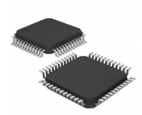


 工商网监
湘ICP备2023018690号
工商网监
湘ICP备2023018690号

