LTC2978A
8-Channel PMBus Power
System Manager Featuring Accurate
Output Voltage Measurement
DESCRIPTION
NOT RECOMMENDED FOR NEW DESIGNS
Please See LTC2977 for Replacement
FEATURES
n
n
n
n
n
n
Sequence, Trim, Margin and Supervise Eight Power Supplies
Manage Faults, Monitor Telemetry and Create Fault Logs
PMBus Compliant Command Set
Supported by LTpowerPlay® GUI
Margin or Trim Supplies to 0.25% Accuracy
Fast OV/UV Supervisors per Channel
Coordinate Sequencing and Fault Management
Across Multiple Chips
n Automatic Fault Logging to Internal EEPROM
n Operate Autonomously without Additional Software
n Internal Temperature and Input Voltage Supervisors
n Accurate Monitoring of Eight Output Voltages, Input
Voltage and Internal Die Temperature
n I2C/SMBus Serial Interface
n Can Be Powered from 3.3V, or 4.5V to 15V
n Programmable Watchdog Timer
n 100% Compatible with the LTC2978
n Available in 64-pin 9mm × 9mm QFN Package
n
APPLICATIONS
n
n
n
n
n
Computers and Network Servers
Industrial Test and Measurement
High Reliability Systems
Medical Imaging
Video
The LTC®2978A is an 8-channel Power System Manager
used to sequence, trim (servo), margin, supervise, manage faults, provide telemetry and create fault logs. PMBus
commands support power supply sequencing, precision
point-of-load voltage adjustment and margining. DACs use
a proprietary soft-connect algorithm to minimize supply
disturbances. Supervisory functions include overvoltage
and undervoltage threshold limits for eight power supply
output channels and one power supply input channel, as
well as over and under temperature limits. Programmable
fault responses can disable the power supplies with optional
retry after a fault is detected. Faults that disable a power
supply can automatically trigger black box EEPROM storage
of fault status and associated telemetry. An internal 16-bit
ADC monitors eight output voltages, one input voltage,
and die temperature. In addition, odd numbered channels can be configured to measure the voltage across a
current sense resistor. A programmable watchdog timer
monitors microprocessor activity for a stalled condition and
resets the microprocessor if necessary. A single wire bus
synchronizes power supplies across multiple ADI power
system management devices. Configuration EEPROM supports autonomous operation without additional software.
All registered trademarks and trademarks are the property of their respective owners. Protected
by U.S. Patents including 7382303, 7420359 and 7940091.
TYPICAL APPLICATION
Typical ADC Total Unadjusted
Error vs Temperature
8-Channel PMBus Power System Manager
VIN_SNS
VPWR
3.3V**
VDD33
TO INTERMEDIATE
BUS CONVERTER ENABLE
VIN_EN
SDA
PMBus
INTERFACE
VDACP0
VSENSEP0
LTC2978A*
SCL
R30
R20
0.035
VOUT
0.030
DIGITALLY
MANAGED
POWER
SUPPLY
VFB
LOAD
VDACM0
VIN
R10
ALERTB
VSENSEM0
SGND
CONTROL0
VOUT_EN0
RUN/SS
GND
WRITE-PROTECT
WP
TO/FROM OTHER
LTC2978s
FAULTB00
PWRGD
WDI/RESETB
ASEL0
SHARE_CLK
ASEL1
GND
2978a TA01a
TO µP RESETB INPUT
WATCHDOG
TIMER INTERRUPT
*SOME DETAILS OMITTED FOR CLARITY
ONLY ONE OF EIGHT CHANNELS SHOWN
ADC VIN = 1.8V
0.025
ERROR (%)
4.5V < VIBUS < 15V**
0.020
0.015
0.010
0.005
0
–50 –35 –20 –5 10 25 40 55 70 85 100
TEMPERATURE (°C)
2978a TA01b
**LTC2978A MAY BE POWERED FROM EITHER AN
EXTERNAL 3.3V SUPPLY OR THE INTERMEDIATE BUS
2978afb
For more information www.linear.com/LTC2978A
1
�LTC2978A
TABLE OF CONTENTS
Features...................................................... 1
Applications................................................. 1
Typical Application......................................... 1
Description.................................................. 1
Absolute Maximum Ratings............................... 4
Order Information........................................... 4
Pin Configuration........................................... 4
Electrical Characteristics.................................. 5
PMBus Timing Diagram.................................... 9
Typical Performance Characteristics................... 10
Pin Functions............................................... 15
Block Diagram.............................................. 17
Operation................................................... 18
Operation Overview................................................. 18
EEPROM.............................................................. 18
Reset....................................................................... 19
Write-Protect Pin..................................................... 19
Other Operations..................................................... 19
Clock Sharing...................................................... 19
PMBus Serial Digital Interface.................................20
PMBus.................................................................20
Device Address....................................................23
Processing Commands........................................ 24
Summary Table....................................................25
PMBus Command Summary............................. 25
Data Formats.......................................................29
PMBus Command Description........................... 30
Operation, Mode and EEPROM Commands.............30
PAGE...................................................................30
OPERATION......................................................... 31
ON_OFF_CONFIG................................................. 32
CLEAR_FAULTS.................................................. 32
WRITE_PROTECT................................................33
STORE_USER_ALL and RESTORE_USER_ALL..33
CAPABILITY.........................................................33
VOUT_MODE.......................................................34
Output Voltage Related Commands.........................34
VOUT_COMMAND, VOUT_MAX, VOUT_MARGIN_
HIGH, VOUT_MARGIN_LOW, VOUT_OV_FAULT_
LIMIT, VOUT_OV_WARN_LIMIT, VOUT_UV_
WARN_LIMIT, VOUT_UV_FAULT_LIMIT, POWER_
GOOD_ON and POWER_GOOD_OFF...................34
2
Input Voltage Related Commands............................34
VIN_ON, VIN_OFF, VIN_OV_FAULT_LIMIT, VIN_
OV_WARN_LIMIT, VIN_UV_WARN_LIMIT and
VIN_UV_FAULT_LIMIT........................................34
Temperature Related Commands.............................35
OT_FAULT_LIMIT, OT_WARN_LIMIT, UT_WARN_
LIMIT and UT_FAULT_LIMIT................................35
Timer Limits............................................................35
TON_DELAY, TON_RISE, TON_MAX_FAULT_
LIMIT and TOFF_DELAY......................................35
Fault Response for Voltages Measured by the High
Speed Supervisor....................................................36
VOUT_OV_FAULT_RESPONSE and VOUT_UV_
FAULT_RESPONSE..............................................36
Fault Response for Values Measured by the ADC.... 37
OT_FAULT_RESPONSE, UT_FAULT_RESPONSE,
VIN_OV_FAULT_RESPONSE and VIN_UV_FAULT_
RESPONSE.......................................................... 37
Timed Fault Response............................................. 37
TON_MAX_FAULT_RESPONSE........................... 37
Status Commands...................................................38
STATUS_BYTE.....................................................38
STATUS_WORD...................................................39
STATUS_VOUT.................................................... 39
STATUS_INPUT...................................................40
STATUS_TEMPERATURE.....................................40
STATUS_CML...................................................... 41
STATUS_MFR_SPECIFIC..................................... 41
ADC Monitoring Commands.................................... 42
READ_VIN........................................................... 42
READ_VOUT........................................................ 42
READ_TEMPERATURE_1 ................................... 42
PMBUS_REVISION.............................................. 42
Manufacturer Specific Commands...........................43
MFR_CONFIG_LTC2978......................................43
MFR_CONFIG_ALL_LTC2978.............................44
MFR_FAULTBz0_PROPAGATE, MFR_FAULTBz1_
PROPAGATE........................................................45
MFR_PWRGD_EN...............................................46
MFR_FAULTB00_RESPONSE, MFR_FAULTB01_
RESPONSE, MFR_FAULTB10_RESPONSE and
MFR_FAULTB11_RESPONSE............................... 47
2978afb
For more information www.linear.com/LTC2978A
�LTC2978A
TABLE OF CONTENTS
MFR_VINEN_OV_FAULT_RESPONSE..................48
MFR_VINEN_UV_FAULT_RESPONSE.................. 49
MFR_RETRY_DELAY........................................... 49
MFR_RESTART_DELAY.......................................50
MFR_VOUT_PEAK...............................................50
MFR_VIN_PEAK..................................................50
MFR_TEMPERATURE_PEAK...............................50
MFR_DAC............................................................ 51
MFR_POWERGOOD_ASSERTION_DELAY.......... 51
Watchdog Operation................................................ 51
MFR_WATCHDOG_T_FIRST and MFR_
WATCHDOG_T..................................................... 51
MFR_PAGE_FF_MASK........................................ 52
MFR_PADS..........................................................53
MFR_I2C_BASE_ADDRESS................................53
MFR_SPECIAL_ID...............................................53
MFR_SPECIAL_LOT............................................54
MFR_VOUT_DISCHARGE_THRESHOLD..............54
MFR_COMMON...................................................54
MFR_SPARE_0, MFR_SPARE_1, MFR_SPARE_2,
MFR_SPARE_3...................................................54
MFR_VOUT_MIN.................................................55
MFR_VIN_MIN....................................................55
MFR_TEMPERATURE_MIN.................................55
Fault Log Operation.................................................55
MFR_FAULT_LOG_STORE..................................56
MFR_FAULT_LOG_RESTORE..............................56
MFR_FAULT_LOG_CLEAR...................................56
MFR_FAULT_LOG_STATUS.................................56
MFR_FAULT_LOG................................................ 57
Applications Information................................. 63
Overview..................................................................63
Powering the LTC2978A..........................................63
Setting Command Register Values..........................63
Sequence, Servo, Margin and Restart Operations...63
Command Units On or Off...................................63
On Sequencing....................................................64
On State Operation..............................................64
Servo Modes.......................................................64
DAC Modes..........................................................65
Margining............................................................65
Off Sequencing....................................................65
VOUT Off Threshold Voltage.................................65
Automatic Restart Via MFR_RESTART_DELAY
Command and CONTROLn pin............................66
Fault Management...................................................66
Output Overvoltage and Undervoltage Faults......66
Output Overvoltage and Undervoltage Warnings.66
Configuring the VIN_EN Output.............................66
Multichannel Fault Management ......................... 67
Interconnect Between Multiple LTC2978A’s.............69
Application Circuits.................................................. 70
Trimming and Margining DC/DC Converters with
External Feedback Resistors............................... 70
Four-Step Resistor Selection Procedure for DC/DC
Converters with External Feedback Resistors..... 71
Trimming and Margining DC/DC Converters with a
TRIM Pin.............................................................72
Two-Step Resistor and DAC Full-Scale Voltage
Selection Procedure for DC/DC Converters with a
TRIM Pin.............................................................72
Measuring Current............................................... 72
Measuring Current with a Sense Resistor...........73
Measuring Current with Inductor DCR................. 73
Single Phase Design Example............................. 74
Measuring Multiphase Currents.......................... 74
Multiphase Design Example................................ 74
Anti-aliasing Filter Considerations....................... 75
Sensing Negative Voltages.................................. 75
Connecting the DC1613 USB to I2C/SMBus/PMBus
Controller to the LTC2978A in System..................... 76
LTpowerPlay: An Interactive GUI for Power System
Managers................................................................. 78
PCB Assembly and Layout Suggestions.................. 79
Bypass Capacitor Placement............................... 79
Exposed Pad Stencil Design................................ 79
PC Board Layout................................................. 79
Unused ADC Sense Inputs................................... 79
Package Description...................................... 80
Revision History........................................... 81
Typical Application........................................ 82
Related Parts............................................... 82
2978afb
For more information www.linear.com/LTC2978A
3
�LTC2978A
Supply Voltages:
VPWR to GND.......................................... –0.3V to 15V
VDD33 to GND........................................ –0.3V to 3.6V
VDD25 to GND...................................... –0.3V to 2.75V
Digital Input/Output Voltages:
ALERTB, SDA, SCL, CONTROL0,
CONTROL1............................................. –0.3V to 5.5V
PWRGD, SHARE_CLK,
WDI/RESETB, WP.....................–0.3V to VDD33 + 0.3V
FAULTB00, FAULTB01, FAULTB10,
FAULTB11.................................–0.3V to VDD33 + 0.3V
ASEL0, ASEL1...........................–0.3V to VDD33 + 0.3V
Analog Voltages:
REFP.................................................... –0.3V to 1.35V
REFM to GND......................................... –0.3V to 0.3V
VIN_SNS to GND...................................... –0.3V to 15V
VSENSEP[7:0] to GND.................................. –0.3V to 6V
VSENSEM[7:0] to GND................................. –0.3V to 6V
VOUT_EN[3:0], VIN_EN to GND................... –0.3V to 15V
VOUT_EN[7:4] to GND.................................. –0.3V to 6V
VDACP[7:0] to GND..................................... –0.3V to 6V
VDACM[7:0] to GND ................................. –0.3V to 0.3V
Operating Junction Temperature Range:
LTC2978AC............................................... 0°C to 70°C
LTC2978AI............................................–40°C to 85°C
Storage Temperature Range................... –65°C to 125°C
Maximum Junction Temperature......................... 125°C*
PIN CONFIGURATION
TOP VIEW
64 VSENSEP6
63 VSENSEM5
62 VSENSEP5
61 VDACM7
60 VDACP7
59 VDACP6
58 VDACM6
57 VDACM5
56 VDACP5
55 VDACP4
54 VDACM4
53 VSENSEM4
52 VSENSEP4
51 VDACM3
50 VDACP3
49 VSENSEM3
(Notes 1, 2)
VSENSEM6 1
VSENSEP7 2
VSENSEM7 3
VOUT_EN0 4
VOUT_EN1 5
VOUT_EN2 6
VOUT_EN3 7
VOUT_EN4 8
VOUT_EN5 9
VOUT_EN6 10
VOUT_EN7 11
VIN_EN 12
DNC 13
VIN_SNS 14
VPWR 15
VDD33 16
65
GND
48 VSENSEP3
47 VSENSEM2
46 VSENSEP2
45 VDACM2
44 VDACP2
43 VSENSEM1
42 VSENSEP1
41 VDACM1
40 VDACP1
39 VDACP0
38 VDACM0
37 VSENSEM0
36 VSENSEP0
35 REFM
34 REFP
33 ASEL1
VDD33 17
VDD25 18
WP 19
PWRGD 20
SHARE_CLK 21
WDI/RESETB 22
FAULTB00 23
FAULTB01 24
FAULTB10 25
FAULTB11 26
SDA 27
SCL 28
ALERTB 29
CONTROL0 30
CONTROL1 31
ASEL0 32
ABSOLUTE MAXIMUM RATINGS
UP PACKAGE
64-LEAD (9mm × 9mm) PLASTIC QFN
TJMAX = 125°C, θJA-TOP = 28°C/W, θJC-BOTTOM = 1°C/W
EXPOSED PAD (PIN 65) IS GND, MUST BE SOLDERED TO PCB
*See OPERATION section for detailed EEPROM derating information for junction temperatures in excess
of 85°C.
ORDER INFORMATION
http://www.linear.com/product/LTC2978A#orderinfo
LEAD FREE FINISH
TAPE AND REEL
PART MARKING*
PACKAGE DESCRIPTION
JUNCTION TEMPERATURE RANGE
LTC2978ACUP#PBF
LTC2978ACUP#TRPBF
LTC2978AUP
64-Lead (9mm × 9mm) Plastic QFN
0°C to 70°C
LTC2978AIUP#PBF
LTC2978AIUP#TRPBF
LTC2978AUP
64-Lead (9mm × 9mm) Plastic QFN
–40°C to 85°C
Consult ADI Marketing for parts specified with wider operating temperature ranges. *The temperature grade is identified by a label on the shipping container.
For more information on lead free part marking, go to: http://www.linear.com/leadfree/
For more information on tape and reel specifications, go to: http://www.linear.com/tapeandreel/. Some packages are available in 500 unit reels through
designated sales channels with #TRMPBF suffix.
4
2978afb
For more information www.linear.com/LTC2978A
�LTC2978A
ELECTRICAL
CHARACTERISTICS
The l denotes the specifications which apply over the full operating
temperature range, otherwise specifications are at TJ = 25°C. VPWR = VIN_SNS = 12V, VDD33, VDD25, REFP and REFM pins floating,
unless otherwise indicated. CVDD33 = 100nF, CVDD25 = 100nF and CREF = 100nF.
SYMBOL
PARAMETER
CONDITIONS
MIN
TYP
MAX
UNITS
15
V
10
13
mA
10
13
mA
2.55
2.8
V
Power-Supply Characteristics
VPWR
VPWR Supply Input Operating Range
IPWR
VPWR Supply Current
4.5V ≤ VPWR ≤ 15V, VDD33 Floating
l
IVDD33
VDD33 Supply Current
3.13V ≤ VDD33 ≤ 3.47V, VPWR = VDD33
l
VUVLO_VDD33
VDD33 Undervoltage Lockout
VDD33 Ramping Up, VPWR = VDD33
l
l
4.5
2.35
VDD33 Undervoltage Lockout
Hysteresis
VDD33
120
Supply Input Operating Range
VPWR = VDD33
l
3.13
Regulator Output Voltage
4.5V ≤ VPWR ≤ 15V
l
3.13
mV
3.47
V
3.26
3.47
V
Regulator Output Short-Circuit Current VPWR = 4.5V, VDD33 = 0V
l
75
90
140
mA
VDD25
Regulator Output Voltage
l
2.35
2.5
2.6
V
l
30
55
80
mA
tINIT
Initialization Time
3.13V ≤ VDD33 ≤ 3.47V
Regulator Output Short-Circuit Current VPWR = VDD33 = 3.47V, VDD25 = 0V
Time from VIN Applied Until the
TON_DELAY Timer Starts
135
ms
Voltage Reference Characteristics
VREF
Output Voltage
VREF = VREFP – VREFM, 0 < IREFP < 100µA
1.232
Temperature Coefficient
Hysteresis
V
3
(Note 3)
ppm/°C
100
ppm
ADC Characteristics
VIN_ADC
Voltage Sense Input Range
Current Sense Input Range (Odd
Numbered Channels Only)
N_ADC
Differential Voltage:
VIN_ADC = (VSENSEPn – VSENSEMn)
l
0
6
V
Single-Ended Voltage: VSENSEMn
l
–0.1
0.1
V
Single-Ended Voltage: VSENSEPn, VSENSEMn
l
–0.1
6
V
Differential Voltage: VIN_ADC
l
–170
170
mV
Voltage Sense Resolution (Uses L16
Format)
0V ≤ VIN_ADC ≤ 6V
Current Sense Resolution (Odd
Numbered Channels Only)
0mV ≤ |VIN_ADC| < 16mV (Note11)
16mV ≤ |VIN_ADC| < 32mV
32mV ≤ |VIN_ADC| < 63.9mV
63.9mV ≤ |VIN_ADC| < 127.9mV
127.9mV ≤ |VIN_ADC|
TUE_ADC_
VOLT_SNS
Total Unadjusted Error
Voltage Sense Mode VIN_ADC ≥ 1V
l
±0.25
Voltage Sense Mode 0 ≤ VIN_ADC ≥ 1V
l
±2.5
mV
TUE_ADC_
CURR_SNS
Total Unadjusted Error
Current Sense Mode, Odd Numbered
Channels Only, 20mV ≤ VIN_ADC ≤ 170mV
l
±0.7
% of
Reading
Current Sense Mode, Odd Numbered
Channels Only, VIN_ADC ≤ 20mV
l
140
µV
l
±35
µV
122
µV/LSB
15.625
31.25
62.5
125
250
µV/LSB
µV/LSB
µV/LSB
µV/LSB
µV/LSB
% of
Reading
VOS_ADC
Offset Error
Current Sense Mode, Odd Numbered
Channels Only
tCONV_ADC
Conversion Time
Voltage Sense Mode (Note 4)
6.15
ms
Current Sense Mode (Note 4)
24.6
ms
Temperature Input (Note 4)
24.6
ms
Odd Numbered Channels in Current Sense
Mode (Note 4)
160
ms
tUPDATE_ADC
Maximum Update Time
2978afb
For more information www.linear.com/LTC2978A
5
�LTC2978A
ELECTRICAL CHARACTERISTICS
The l denotes the specifications which apply over the full operating
temperature range, otherwise specifications are at TJ = 25°C. VPWR = VIN_SNS = 12V; VDD33, VDD25, REFP and REFM pins floating,
unless otherwise indicated. CVDD33 = 100nF, CVDD25 = 100nF and CREF = 100nF.
SYMBOL
PARAMETER
CONDITIONS
MIN
CIN_ADC
Input Sampling Capacitance
fIN_ADC
Input Sampling Frequency
IIN_ADC
Input Leakage Current
VIN_ADC = 0V, 0V ≤ VCOMMONMODE ≤ 6V,
Current Sense Mode
l
Differential Input Current
VIN_ADC = 0.17V, Current Sense Mode
l
VIN_ADC = 6V, Voltage Sense Mode
l
TYP
MAX
UNITS
1
pF
62.5
kHz
±0.5
µA
80
250
nA
10
15
µA
DAC Output Characteristics
N_VDACP
Resolution
VFS_VDACP
Full-Scale Output Voltage
(Programmable)
DAC Code = 0x3FF Buffer Gain Setting_0
DAC Polarity = 1
Buffer Gain Setting_1
l
l
10
1.32
2.53
1.38
2.65
Bits
1.44
2.77
V
V
INL_VDACP
Integral Nonlinearity
(Note 5)
l
±2
LSB
DNL_VDACP
Differential Nonlinearity
(Note 5)
l
±2.4
LSB
VOS_VDACP
Offset Voltage
(Note 5)
l
VDACP
Load Regulation (VDACPn – VDACMn)
VDACPn = 2.65V, IVDACPn Sourcing = 2mA
100
ppm/mA
VDACPn = 0.1V, IVDACPn Sinking = 2mA
100
ppm/mA
PSRR (VDACPn – VDACMn)
DC: 3.13V ≤ VDD33 ≤ 3.47V, VPWR = VDD33
60
dB
100mV Step in 20ns with 50pF Load
40
dB
DC CMRR (VDACPn – VDACMn)
–0.1V ≤ VDACMn ≤ 0.1V
60
dB
±10
Leakage Current
VDACPn Hi-Z, 0V ≤ VDACPn ≤ 6V
l
Short-Circuit Current Low
VDACPn Shorted to GND
l
–10
l
4
mV
±100
nA
–4
mA
10
mA
Short-Circuit Current High
VDACPn Shorted to VDD33
COUT
Output Capacitance
VDACPn Hi-Z
10
pF
tS_VDACP
DAC Output Update Rate
Fast Servo Mode
250
µs
Voltage Supervisor Characteristics
VIN_VS
N_VS
TUE_VS
tS_VS
Input Voltage Range (Programmable)
Voltage Sensing Resolution
Total Unadjusted Error
VIN_VS = (VSENSEPn Low Resolution Mode
– VSENSEMn)
High Resolution Mode
l
l
0
0
6
3.8
V
V
Single-Ended Voltage: VSENSEMn
l
–0.1
0.1
V
0V to 3.8V Range: High Resolution Mode
4
mV/LSB
0V to 6V Range: Low Resolution Mode
8
mV/LSB
2V ≤ VIN_VS ≤ 6V, Low Resolution Mode
l
±1.25
%
1.5V < VIN_VS ≤ 3.8V, High Resolution
Mode
l
±1.0
%
0.8V ≤ VIN_VS ≤ 1.5V, High Resolution
Mode
l
±1.5
%
Update Rate
12.21
µs
VIN_SNS Input Characteristics
VVIN_SNS
VIN_SNS Input Voltage Range
RVIN_SNS
VIN_SNS Input Resistance
TUEVIN_SNS
VIN_ON, VIN_OFF Threshold Total
Unadjusted Error
3V ≤ VVIN_SNS ≤ 8V
l
VVIN_SNS > 8V
l
±1.0
%
READ_VIN Total Unadjusted Error
3V ≤ VVIN_SNS ≤ 8V
l
±1.5
%
VVIN_SNS > 8V
l
±1.0
%
6
l
0
l
70
90
15
V
110
kΩ
±2.0
%
2978afb
For more information www.linear.com/LTC2978A
�LTC2978A
ELECTRICAL CHARACTERISTICS
The l denotes the specifications which apply over the full operating
temperature range, otherwise specifications are at TJ = 25°C. VPWR = VIN_SNS = 12V; VDD33, VDD25, REFP and REFM pins floating,
unless otherwise indicated. CVDD33 = 100nF, CVDD25 = 100nF and CREF = 100nF.
SYMBOL
PARAMETER
CONDITIONS
MIN
TYP
MAX
UNITS
DAC Soft-Connect Comparator Characteristics
VOS_CMP
Offset Voltage
VDACPn = 0.2V
l
±1
±18
mV
VDACPn = 1.3V
l
±2
±26
mV
VDACPn = 2.65V
l
±3
±52
mV
Temperature Sensor Characteristics
TUE_TS
Total Unadjusted Error
±1
°C
VOUT Enable Output (VOUT_EN [3:0]) Characteristics
VVOUT_ENn
Output High Voltage (Note 10)
IVOUT_ENn = –5µA, VDD33 = 3.3V
l
10
12.5
14.7
IVOUT_ENn
Output Sourcing Current
VVOUT_ENn Pull-Up Enabled, VVOUT_ENn = 1V l
–5
–6
–8
µA
Output Sinking Current
Strong Pull-Down Enabled,
VVOUT_ENn = 0.4V
l
3
5
8
mA
Weak Pull-Down Enabled, VVOUT_ENn = 0.4V l
33
50
60
µA
±1
µA
9
mA
±1
µA
V
Output Leakage Current
Internal Pull-Up Disabled,
0V ≤ VVOUT_ENn ≤ 15V
l
Output Sinking Current
Strong Pull-Down Enabled,
VOUT_ENn = 0.1V
l
Output Leakage Current
0V ≤ VVOUT_ENn ≤ 6V
l
V
VOUT Enable Output (VOUT_EN [7:4]) Characteristics
IVOUT_ENn
3
6
VIN Enable Output (VIN_EN) Characteristics
VVIN_EN
Output High Voltage
IVIN_EN = –5µA, VDD33 = 3.3V
l
10
12.5
14.7
IVIN_EN
Output Sourcing Current
VIN_EN Pull-Up Enabled, VVIN_EN = 1V
l
–5
–6
–8
µA
Output Sinking Current
VVIN_EN = 0.4V
l
3
5
8
mA
Leakage Current
Internal Pull-Up Disabled,
0V ≤ VVIN_EN ≤ 15V
l
±1
µA
EEPROM Characteristics
Endurance
(Notes 6, 9)
0°C < TJ < 85°C During EEPROM Write
Operations
l
10,000
Retention
(Notes 6, 9)
TJ < 85°C
l
10
tMASS_WRITE
Mass Write Operation Time (Note 7)
STORE_USER_ALL, 0°C < TJ < 85°C During l
EEPROM Write Operations
Cycles
Years
440
4100
ms
Digital Inputs SCL, SDA, CONTROL0, CONTROL1, WDI/RESETB, FAULTB00, FAULTB01, FAULTB10, FAULTB11, WP
VIH
High Level Input Voltage
l
VIL
Low Level Input Voltage
l
VHYST
Input Hysteresis
ILEAK
Input Leakage Current
2.1
V
1.5
20
V
mV
0V ≤ VPIN ≤ 5.5V, SDA, SCL, CONTROLn
Pins Only
l
±2
µA
0V ≤ VPIN ≤ VDD33 + 0.3V, FAULTBzn,
WDI/RESETB, WP Pins Only
l
±2
µA
tSP
Pulse Width of Spike Suppressed
FAULTBzn, CONTROLn Pins Only
tFAULT_MIN
Minimum Low Pulse Width for
Externally Generated Faults
tRESETB
Pulse Width to Assert Reset
VWDI/RESETB ≤ 1.5V
tWDI
Pulse Width to Reset Watchdog Timer
VWDI/RESETB ≤ 1.5V
10
SDA, SCL Pins Only
µs
98
ns
110
ms
l
300
µs
l
0.3
200
µs
2978afb
For more information www.linear.com/LTC2978A
7
�LTC2978A
ELECTRICAL CHARACTERISTICS
The l denotes the specifications which apply over the full operating
temperature range, otherwise specifications are at TJ = 25°C. VPWR = VIN_SNS = 12V; VDD33, VDD25, REFP and REFM pins floating,
unless otherwise indicated. CVDD33 = 100nF, CVDD25 = 100nF and CREF = 100nF.
SYMBOL
PARAMETER
fWDI
Watchdog Interrupt Input Frequency
CIN
Digital Input Capacitance
CONDITIONS
MIN
TYP
MAX
1
l
10
UNITS
MHz
pF
Digital Input SHARE_CLK
VIH
High Level Input Voltage
l
VIL
Low Level Input Voltage
l
fSHARE_CLK_IN Input Frequency Operating Range
1.6
l
90
0.825
tLOW
Assertion Low Time
VSHARE_CLK < 0.8V
l
tRISE
Rise Time
VSHARE_CLK < 0.8V to VSHARE_CLK > 1.6V
l
ILEAK
Input Leakage Current
0V ≤ VSHARE_CLK ≤ VDD33 + 0.3V
l
CIN
Input Capacitance
V
0.8
V
110
kHz
1.1
µs
450
ns
±1
µA
10
pF
Digital Outputs SDA, ALERTB, PWRGD, SHARE_CLK, FAULTB00, FAULTB01, FAULTB10, FAULTB11
VOL
Digital Output Low Voltage
fSHARE_CLK_OUT Output Frequency Operating Range
ISINK = 3mA
l
5.49kΩ Pull-Up to VDD33
l
90
VDD33 – 0.5
100
0.4
V
110
kHz
Digital Inputs ASEL0,ASEL1
VIH
Input High Threshold Voltage
l
VIL
Input Low Threshold Voltage
l
0.5
V
IIH,IL
High, Low Input Current
l
±95
µA
IIH, Z
Hi-Z Input Current
±24
µA
CIN
Input Capacitance
ASEL[1:0] = 0, VDD33
V
l
10
pF
Serial Bus Timing Characteristics
fSCL
Serial Clock Frequency (Note 8)
l
10
400
kHz
tLOW
Serial Clock Low Period (Note 8)
l
1.3
µs
tHIGH
Serial Clock High Period (Note 8)
l
0.6
µs
tBUF
Bus Free Time Between Stop and Start
(Note 8)
l
1.3
µs
tHD,STA
Start Condition Hold Time (Note 8)
l
600
ns
tSU,STA
Start Condition Setup Time (Note 8)
l
600
ns
tSU,STO
Stop Condition Setup Time (Note 8)
l
600
ns
tHD,DAT
Data Hold Time (LTC2978A Receiving
Data) (Note 8)
l
0
ns
Data Hold Time (LTC2978A
Transmitting Data) (Note 8)
l
300
tSU,DAT
Data Setup Time (Note 8)
l
100
tSP
Pulse Width of Spike Suppressed
(Note 8)
tTIMEOUT_BUS
Time Allowed to Complete any PMBus Longer Timeout = 0
Command after Which Time SDA Will Longer Timeout = 1
Be Released and Command Terminated
900
ns
98
l
l
ns
25
200
ns
35
280
ms
ms
Additional Digital Timing Characteristics
tOFF_MIN
8
Minimum Off-Time for Any Channel
100
ms
2978afb
For more information www.linear.com/LTC2978A
�LTC2978A
ELECTRICAL CHARACTERISTICS
Note 1: Stresses beyond those listed under Absolute Maximum Ratings may
cause permanent damage to the device. Exposure to any Absolute Maximum
Rating for extended periods may affect device reliability and lifetime.
Note 2: All currents into device pins are positive. All currents out of device
pins are negative. All voltages are referenced to ground unless otherwise
specified. If power is supplied to the chip via the VDD33 pin only, connect
VPWR and VDD33 pins together.
Note 3: Hysteresis in the output voltage is created by package stress that
differs depending on whether the IC was previously at a higher or lower
temperature. Output voltage is always measured at 25°C, but the IC is
cycled to 85°C or –40°C before successive measurements. Hysteresis is
roughly proportional to the square of the temperature change.
Note 4: The time between successive ADC conversions (latency of the
ADC) for any given channel is given as: 36.9ms + (6.15ms • number of
ADC channels configured in Low Resolution mode) + (24.6ms • number of
ADC channels configured in High Resolution mode).
Note 5: Nonlinearity is defined from the first code that is greater than or
equal to the maximum offset specification to full-scale code, 1023.
Note 6: EEPROM endurance and retention are guaranteed by design,
characterization and correlation with statistical process controls. The
minimum retention specification applies for devices whose EEPROM has
been cycled less than the minimum endurance specification.
Note 7: The LTC2978A will not acknowledge any PMBus commands while
a mass write operation is being executed. This includes the STORE_USER_
ALL and MFR_FAULT_LOG_STORE commands or a fault log store initiated
by a channel faulting off.
Note 8: Maximum capacitive load, CB, for SCL and SDA is 400pF. Data and
clock rise time (tr) and fall time (tf) are: (20 + 0.1 • CB) (ns) < tr < 300ns and
(20 + 0.1 • CB) (ns) < tf < 300ns. CB = capacitance of one bus line in pF. SCL
and SDA external pull-up voltage, VIO, is 3.13V < VIO < 5.5V.
Note 9: EEPROM endurance and retention will be degraded when TJ > 85°C.
Note 10: Output enable pins are charge-pumped from VDD33.
Note 11: The current sense resolution is determined by the L11 format
and the mV units of the returned value. For example a full scale value
of 170mV returns an L11 value of 0xF2A8 = 680 • 2–2 = 170. This is the
lowest range that can represent this value without overflowing the L11
mantissa and the resolution for 1LSB in this range is 2–2 mV = 250µV.
Each successively lower range improves resolution by cutting the LSB size
in half.
PMBUS TIMING DIAGRAM
SDA
tf
tLOW
tr
tSU(DAT)
tHD(SDA)
tf
tSP
tr
tBUF
SCL
tHD(STA)
START
CONDITION
tHD(DAT)
tHIGH
tSU(STA)
tSU(STO)
2978a TD
REPEATED START
CONDITION
STOP
CONDITION
START
CONDITION
2978afb
For more information www.linear.com/LTC2978A
9
�LTC2978A
TYPICAL PERFORMANCE CHARACTERISTICS
ADC Total Unadjusted Error
vs Temperature
Temperature Sensor Error
vs Temperature
Reference Voltage vs Temperature
1.6
0.035
1.2350
1.4
0.030
REFERENCE OUTPUT VOLTAGE (V)
1.2355
1.2345
1.2
1.2340
ERROR (%)
1.2330
0.025
1.0
ERROR (°C)
1.2335
0.8
0.6
1.2325
THREE TYPICAL PARTS
1.2310
–50 –35 –20 –5 10 25 40 55 70 85 100
TEMPERATURE (°C)
0
–50 –35 –20 –5 10 25 40 55 70 85 100
TEMPERATURE (°C)
ADC Zero Code Center Offset
Voltage vs Temperature
VOLTAGE SENSE MODE
ADC-DNL
0.8
122µV/LSB
0.6
2.5
–40
2.0
0.4
–60
1.5
0.2
–80
–100
ERROR (LSBs)
–20
ERROR (LSBs)
VOS (µV)
2978a G03
ADC-INL
3.0
–120
1.0
0
–0.4
0
–140
–0.5
–0.6
–160
–1.0
–0.8
–180
–50 –35 –20 –5 10 25 40 55 70 85 100
TEMPERATURE (°C)
–1.5
–0.2
0
0.8
1.8
2.8
3.8
4.8
INPUT VOLTAGE (V)
5.8
–1.0
–0.2
0
ADC Rejection
vs Frequency at VIN (Zoom)
0
–40
–40
–40
–120
REJECTION (dB)
–20
REJECTION (dB)
–20
–100
–60
–80
12500
25000 37500 50000
FREQUENCY (Hz)
62500
2978a G07
10
–120
5.8
ADC Rejection vs Frequency
at VIN (Current Sense Mode)
–60
–80
–100
–100
0
1.8
2.8
3.8
4.8
INPUT VOLTAGE (V)
2978a G06
–20
–80
0.8
2978a G05
ADC Rejection
vs Frequency at VIN
–60
122µV/LSB
–0.2
0.5
2978a G04
REJECTION (dB)
0
–50 –35 –20 –5 10 25 40 55 70 85 100
TEMPERATURE (°C)
2978a G02
2978a G01
0
0.015
0.005
0.2
1.2315
0.020
0.010
0.4
1.2320
ADC VIN = 1.8V
0
3125
6250
9375
FREQUENCY (Hz)
12500
2978a G08
–120
0
12500
25000 37500 50000
FREQUENCY (Hz)
62500
2978a G09
2978afb
For more information www.linear.com/LTC2978A
�LTC2978A
TYPICAL PERFORMANCE CHARACTERISTICS
1200
NUMBER OF READINGS
REJECTION (dB)
–60
–80
0
3125
6250
9375
FREQUENCY (Hz)
–0.10
800
600
400
–0.25
–10
0
10
READ_VOUT (µV)
–0.40
–50 –35 –20 –5 10 25 40 55 70 85 100
TEMPERATURE (°C)
20
2978a G11
Input Sampling Current
vs Differential Input Voltage
2978a G12
DAC Full-Scale Output Voltage vs
Temperature
ADC High Resolution Mode
Differential Input Current
9
90
2.698
8
80
2.696
7
6
5
4
3
2
1
0
0
1
2
3
4
INPUT VOLTAGE (V)
5
60
50
40
30
2.692
2.690
2.688
2.686
2.684
20
2.682
10
2.680
0
6
2.694
70
OUTPUT VOLTAGE (V)
DIFFERENTIAL INPUT CURRENT (nA)
INPUT SAMPLING CURRENT (µA)
–0.20
–0.35
2978a G10
0
2.678
–50 –35 –20 –5 10 25 40 55 70 85 100
TEMPERATURE (°C)
20 40 60 80 100 120 140 160 180
DIFFERENTIAL INPUT VOLTAGE (mV)
2978a G13
2978a G15
2978a G14
DAC Offset Voltage vs
Temperature
DAC-INL
DAC-DNL
1.0
1.0
2.3
0.8
0.8
2.1
0.6
0.6
1.9
0.4
0.4
1.7
1.5
1.3
ERROR (LSBs)
2.5
ERROR (LSBs)
OFFSET ERROR (mV)
–0.15
–0.30
0
–20
12500
VIN = 0.8V
HIGH RESOLUTION MODE
–0.05
200
–100
–120
0
VIN = 0V
HIGH RESOLUTION MODE
1000
–20
–40
Voltage Supervisor Total
Unadjusted Error vs Temperature
ADC Noise Histogram
ERROR (%)
0
ADC Rejection vs Frequency
at VIN (Current Sense Mode, Zoom)
0.2
0
–0.2
0.2
0
–0.2
1.1
–0.4
–0.4
0.9
–0.6
–0.6
0.7
–0.8
–0.8
0.5
–50 –35 –20 –5 10 25 40 55 70 85 100
TEMPERATURE (°C)
–1.0
2978a G16
0
200
600
400
DAC CODE
800
1000
2978a G17
–1.0
0
200
600
400
DAC CODE
800
1000
2978a G18
2978afb
For more information www.linear.com/LTC2978A
11
�LTC2978A
TYPICAL PERFORMANCE CHARACTERISTICS
DAC Load Regulation (Sourcing)
85°C
2.696
25°C
2.692
OUTPUT VOLTAGE (V)
OUTPUT VOLTAGE (V)
2.694
2.690
2.688
2.686
2.684
2.682
2.678
9.00
0.1036
8.95
85°C
0.1034
25°C
0.1032
0.1030
–40°C
0.1028
–40°C
2.680
0.1038
0 –0.25 –0.5 –0.75 –1 –1.25 –1.50 1.75
CURRENT (mA)
–2
SHORT-CIRCUIT CURRENT (mA)
2.698
DAC Short-Circuit Current vs
Temperature
DAC Load Regulation (Sinking)
0.1026
0
0.25 0.5 0.75 1 1.25 1.5 1.75
CURRENT (mA)
2978a G19
2
8.90
8.85
8.80
8.75
8.70
–50 –35 –20 –5 10 25 40 55 70 85 100
TEMPERATURE (°C)
2978a G21
2978a G20
DAC Soft-Connect Transient
Response when Transitioning from
Hi-Z State to ON State
DAC Transient Response to 1LSB
DAC Code Change
DAC Soft-Connect Transient
Response when Transitioning from
ON State to Hi-Z State
CODE ‘h200
HI-Z
500µV/DIV
CONNECTED
CODE ‘h1FF
2µs/DIV
12
HI-Z
10mV/DIV
10mV/DIV
2978a G22
500µs/DIV
100k SERIES RESISTANCE ON
CODE: ‘h1FF
2978a G23
CONNECTED
500µs/DIV
100k SERIES RESISTANCE ON
CODE: ‘h1FF
2978a G24
2978afb
For more information www.linear.com/LTC2978A
�LTC2978A
TYPICAL PERFORMANCE CHARACTERISTICS
VDD33 Regulator Output Voltage
vs Temperature
–86
400
300
3.265
200
3.260
3.255
3.250
3.245
85°C
25°C
100
–40°C
0
–100
–200
–300
3.240
–400
3.235
–50 –35 –20 –5 10 25 40 55 70 85 100
TEMPERATURE (°C)
–500
4.5
6
7.5
SUPPLY CURRENT (mA)
SUPPLY CURRENT (mA)
9
10.5
VPWR (V)
12
13.5
15
9.9
10.12
10.10
10.08
10.06
3.1
3.2
3.3
3.4
3.5
3.6
VDD33 (V)
2978a G28
–102
–50 –35 –20 –5 10 25 40 55 70 85 100
TEMPERATURE (°C)
2978a G27
VOUT_EN[3:0] and VIN_EN Output
High Voltage vs Load Current
13.5
85°C
13.0
25°C
12.5
–40°C
12.0
11.5
11.0
10.5
10.04
3
–98
14.0
VPWR = 12V
10.14
10.4
10.0
–96
CHARGE PUMP OUTUPT HIGH VOLTAGE (V)
10.16
10.1
–94
Supply Current vs Temperature
VPWR = VDD33
10.2
–92
2978a G26
Supply Current vs Supply Voltage
10.3
–90
–100
2978a G25
10.5
–88
SHORT-CIRCUIT CURRENT (mA)
3.270
∆VDD33 (ppm)
VDD33 OUTPUT VOLTAGE (V)
3.275
9.8
VDD33 Regulator Short-Circuit
Current vs Temperature
VDD33 Regulator Line Regulation
10.02
–50 –35 –20 –5 10 25 40 55 70 85 100
TEMPERATURE (°C)
2978a G29
10.0
9.5
0
1
2
3
4
5
CURRENT SOURCING (µA)
6
7
2978a G30
2978afb
For more information www.linear.com/LTC2978A
13
�LTC2978A
TYPICAL PERFORMANCE CHARACTERISTICS
VOUT_EN[3:0] and VIN_EN VOL
vs Current
DAC Output Impedance vs
Frequency
100
VOUT_EN[7:4] VOL vs Current
1.4
0.6
1.2
0.5
1.0
1
0.4
85°C
0.8
25°C
0.6
0.01
0.01
10
1
FREQUENCY (kHz)
100
–40°C
0.1
0
1000
0
2
4
8
6
ISINK (mA)
4
8
12
16
ISINK (mA)
20
24
2978a G33
ALERTB VOL vs Current
1.2
1.4
1.0
1.2
1.0
VOLTS (V)
0.8
VOLTS (V)
0
2978a G32
PWRGD and FAULTBzn VOL
vs Current
0.6
0.4
85°C
0.8
25°C
0.6
–40°C
0.4
85°C
25°C
–40°C
0.2
0
2
4
6
8
ISINK (mA)
10
0.2
12
0
0
2978a G34
14
0
12
10
2978a G31
0
25°C
0.2
0.2
0.1
85°C
0.3
–40°C
0.4
0.1
VOLTS (V)
10
VOLTS (V)
OUTPUT IMPEDANCE (Ω)
1000
2
4
8
6
ISINK (mA)
10
12
2978a G35
2978afb
For more information www.linear.com/LTC2978A
�LTC2978A
PIN FUNCTIONS
PIN NAME
VSENSEM6
VSENSEP7
VSENSEM7
VOUT_EN0
VOUT_EN1
VOUT_EN2
VOUT_EN3
VOUT_EN4
VOUT_EN5
VOUT_EN6
VOUT_EN7
VIN_EN
DNC
VIN_SNS
PIN NUMBER
PIN TYPE
1*
In
2*
In
3*
In
4
Out
5
Out
6
Out
7
Out
8
Out
9
Out
10
Out
11
Out
12
0ut
13
Do Not Connect
14
In
VPWR
15
In
VDD33
16
In/Out
VDD33
VDD25
WP
PWRGD
17
18
19
20
In
In/Out
In
Out
SHARE_CLK
WDI/RESETB
21
22
In/Out
In
FAULTB00
23
In/Out
FAULTB01
24
In/Out
FAULTB10
25
In/Out
FAULTB11
26
In/Out
SDA
SCL
ALERTB
CONTROL0
CONTROL1
ASEL0
ASEL1
REFP
REFM
VSENSEP0
VSENSEM0
VDACM0
VDACP0
VDACP1
27
28
29
30
31
32
33
34
35
36*
37*
38*
39
40
In/Out
In
Out
In
In
In
In
Out
Out
In
In
Out
Out
Out
DESCRIPTION
DC/DC Converter Differential (–) Output Voltage-6 Sensing Pin
DC/DC Converter Differential (+) Output Voltage or Current-7 Sensing Pin
DC/DC Converter Differential (–) Output Voltage or Current-7 Sensing Pin
DC/DC Converter Enable-0 Pin. Output High Voltage Optionally Pulled Up to 12V by 5µA
DC/DC Converter Enable-1 Pin. Output High Voltage Optionally Pulled Up to 12V by 5µA
DC/DC Converter Enable-2 Pin. Output High Voltage Optionally Pulled Up to 12V by 5µA
DC/DC Converter Enable-3 Pin. Output High Voltage Optionally Pulled Up to 12V by 5µA
DC/DC Converter Open-Drain Pull-Down Output-4
DC/DC Converter Open-Drain Pull-Down Output-5
DC/DC Converter Open-Drain Pull-Down Output-6
DC/DC Converter Open-Drain Pull-Down Output-7
DC/DC Converter VIN ENABLE Pin. Output High Voltage Optionally Pulled Up to 12V by 5µA
Do Not Connect to This Pin
VIN SENSE Input. This Voltage is Compared Against the VIN On and Off Voltage Thresholds in Order to
Determine When to Enable and Disable, Respectively, the Downstream DC/DC Converters
VPWR Serves as the Unregulated Power Supply Input to the Chip (4.5V to 15V). If a 4.5V to 15V Supply
Voltage is Unavailable, Short VPWR to VDD33 and Power the Chip Directly from a 3.3V Supply. Bypass to
GND with 0.1µF Capacitor.
If Shorted to VPWR, it Serves as 3.13V to 3.47V Supply Input Pin. Otherwise it is a 3.3V Internally
Regulated Voltage Output (Use 0.1µF Decoupling Capacitor to GND)
Input for Internal 2.5V Sub-Regulator. Short This Pin to Pin 16
2.5V Internally Regulated Voltage Output. Bypass to GND with a 0.1µF Capacitor
Digital Input. Write-Protect Input Pin, Active High
Power Good Open-Drain Output. Indicates When Outputs are Power Good. Can be Used as System
Power-On Reset. The Latency of This Signal May Be as Long as the ADC Latency. See Note 4.
Bidirectional Clock Sharing Pin. Connect a 5.49k Pull-Up Resistor to VDD33
Watchdog Timer Interrupt and Chip Reset Input. Connect a 10k Pull-Up Resistor to VDD33. Rising Edge
Resets Watchdog Counter. Holding This Pin Low for More Than tRESETB Resets the Chip
Open-Drain Output and Digital Input. Active Low Bidirectional Fault Indicator-00. Connect a 10k Pull-Up
Resistor to VDD33
Open-Drain Output and Digital Input. Active Low Bidirectional Fault Indicator-01. Connect a 10k Pull-Up
Resistor to VDD33
Open-Drain Output and Digital Input. Active Low Bidirectional Fault Indicator-10. Connect a 10k Pull-Up
Resistor to VDD33
Open-Drain Output and Digital Input. Active Low Bidirectional Fault Indicator-11. Connect a 10k Pull-Up
Resistor to VDD33
PMBus Bidirectional Serial Data Pin
PMBus Serial Clock Input Pin (400kHz Maximum)
Open-Drain Output. Generates an Interrupt Request in a Fault/Warning Situation
Control Pin 0 Input
Control Pin 1 Input
Ternary Address Select Pin 0 Input. Connect to VDD33, GND or Float to Encode 1 of 3 Logic States
Ternary Address Select Pin 1 Input. Connect to VDD33, GND or Float to Encode 1 of 3 Logic States
Reference Voltage Output. Needs 0.1µF Decoupling Capacitor to REFM
Reference Return Pin. Needs 0.1µF Decoupling Capacitor to REFP.
DC/DC Converter Differential (+) Output Voltage-0 Sensing Pin
DC/DC Converter Differential (–) Output Voltage-0 Sensing Pin
DAC0 Return. Connect to Channel 0 DC/DC Converter’s GND Sense or Return to GND
DAC0 Output
DAC1 Output
2978afb
For more information www.linear.com/LTC2978A
15
�LTC2978A
PIN FUNCTIONS
PIN NAME
PIN NUMBER
PIN TYPE
DESCRIPTION
41*
Out
DAC1 Return. Connect to Channel 1 DC/DC Converter’s GND Sense or Return to GND
VDACM1
42*
In
DC/DC Converter Differential (+) Output Voltage or Current-1 Sensing Pins
VSENSEP1
43*
In
DC/DC Converter Differential (–) Output Voltage or Current-1 Sensing Pins
VSENSEM1
44
Out
DAC2 Output
VDACP2
45*
Out
DAC2 Return. Connect to Channel 2 DC/DC Converter’s GND Sense or Return to GND
VDACM2
46*
In
DC/DC Converter Differential (+) Output Voltage-2 Sensing Pin
VSENSEP2
47*
In
DC/DC Converter Differential (–) Output Voltage-2 Sensing Pin
VSENSEM2
48*
In
DC/DC Converter Differential (+) Output Voltage or Current-3 Sensing Pins
VSENSEP3
49*
In
DC/DC Converter Differential (–) Output Voltage or Current-3 Sensing Pins
VSENSEM3
50
Out
DAC3 Output
VDACP3
51*
Out
DAC3 Return. Connect to Channel 3 DC/DC Converter’s GND Sense or Return to GND
VDACM3
52*
In
DC/DC Converter Differential (+) Output Voltage-4 Sensing Pin
VSENSEP4
53*
In
DC/DC Converter Differential (–) Output Voltage-4 Sensing Pin
VSENSEM4
54*
Out
DAC4 Return. Connect to Channel 4 DC/DC Converter’s GND Sense or Return to GND
VDACM4
55
Out
DAC4 Output
VDACP4
56
Out
DAC5 Output
VDACP5
57*
Out
DAC5 Return. Connect to Channel 5 DC/DC Converter’s GND Sense or Return to GND
VDACM5
58*
Out
DAC6 Return. Connect to Channel 6 DC/DC Converter’s GND Sense or Return to GND
VDACM6
59
Out
DAC6 Output
VDACP6
60
Out
DAC7 Output
VDACP7
61*
Out
DAC7 Return. Connect to Channel 7 DC/DC Converter’s GND Sense or Return to GND
VDACM7
62*
In
DC/DC Converter Differential (+) Output Voltage or Current-5 Sensing Pins
VSENSEP5
63*
In
DC/DC Converter Differential (–) Output Voltage or Current-5 Sensing Pins
VSENSEM5
64*
In
DC/DC Converter Differential (+) Output Voltage-6 Sensing Pin
VSENSEP6
GND
65
Ground
Exposed Pad, Must be Soldered to PCB
*Any unused VSENSEPn or VSENSEMn or VDACMn pins must be tied to GND.
16
2978afb
For more information www.linear.com/LTC2978A
�LTC2978A
BLOCK DIAGRAM
3.3V REGULATOR
VOUT
VIN
VPWR 15
VDD
VDD33 16
2.5V REGULATOR
VIN
VOUT
VIN_SNS 14
3R
VSENSEM0
VSENSEP0
R
VSENSEM1
GND 65
INTERNAL
TEMP
SENSOR
VSENSEP1
36 VSENSEP0
VSENSEM2
37 VSENSEM0
VSENSEP2
42 VSENSEP1
VSENSEM3
43 VSENSEM1
VSENSEP3
46 VSENSEP2
VSENSEM4
MUX
VSENSEP4
CMP0
VSENSEM5
VSENSEP5
+
–
+
–
VDD33 17
VDD25 18
47 VSENSEM2
+
–
48 VSENSEP3
10-BIT
DAC
49 VSENSEM3
52 VSENSEP4
VSENSEM6
53 VSENSEM4
VSENSEP6
62 VSENSEP5
VSENSEM7
63 VSENSEM5
VSENSEP7
64 VSENSEP6
+ 16-BIT
– ∆∑ ADC
1 VSENSEM6
2 VSENSEP7
3 VSENSEM7
ADC
CLOCKS
10-BIT
DAC
VDD
+
–
39 VDACP0
VBUF
40 VDACP1
44 VDACP2
50 VDACP3
REFERENCE
1.232V
(TYP)
REFP 34
55 VDACP4
56 VDACP5
REFM 35
59 VDACP6
60 VDACP7
38 VDACM0
41 VDACM1
SDA 27
ALERTB 29
ASEL0 32
45 VDACM2
NONVOLATILE MEMORY
SCL 28
PMBus
INTERFACE
(400kHz I2C
COMPATIBLE)
ASEL1 33
54 VDACM4
57 VDACM5
RAM
ADC_RESULTS
MONITOR LIMITS
SERVO TARGETS
58 VDACM6
PAGE 7
WP 19
OUTPUT
CONFIG
CONTROL1 31
OSCILLATOR
WDI/RESETB 22
FAULTB01 24
FAULTB10 25
FAULTB11 26
61 VDACM7
4 VOUT_EN0
CONTROL0 30
FAULTB00 23
51 VDACM3
PAGE 0
EEPROM
CONTROLLER
PMBus ALGORITHM
FAULT PROCESSOR
WATCHDOG
SEQUENCER
CLOCK
GENERATION
UVLO
8 PAGES
PWRGD 20
6 VOUT_EN2
7 VOUT_EN3
12 VIN_EN
VDD
8 PAGES
5 VOUT_EN1
8 VOUT_EN4
OPEN-DRAIN
OUTPUT
9 VOUT_EN5
10 VOUT_EN6
11 VOUT_EN7
SHARE_CLK 21
2978a BD
2978afb
For more information www.linear.com/LTC2978A
17
�LTC2978A
OPERATION
OPERATION OVERVIEW
n
The LTC2978A is a PMBus programmable power system
controller, monitor, sequencer and voltage supervisor that
can perform the following operations:
n
Accept PMBus compatible programming commands.
n
n
Provide DC/DC converter input voltage and output voltage/current read back through the PMBus interface.
n
Control the output of DC/DC converters that set the
output voltage with a trim pin or DC/DC converters
that set the output voltage using an external resistor
feedback network.
n
Sequence the start-up of DC/DC converters via PMBus
programming and their control input pins.
n
Trim the DC/DC converter output voltage (typically in
0.02% steps), in closed-loop servo operating mode,
through PMBus programming.
n
Margin the DC/DC converter output voltage to PMBus
programmed limits.
n
Allow the user to trim or margin the DC/DC converter
output voltage in a manual operating mode by providing
direct access to the margin DAC.
n
Supervise the DC/DC converter output voltage, input
voltage, and the LTC2978A die temperature for overvalue/undervalue conditions with respect to PMBus
programmed limits and generate appropriate faults and
warnings.
n
Respond to a fault condition by either continuing operation indefinitely, latching off after a programmable
deglitch period or latching off immediately. A retry mode
may be used to automatically recover from a latched-off
condition.
n
Optionally stop trimming the DC/DC converter output
voltage after it reached the initial margin or nominal
target. Optionally allow servo to resume if target drifts
outside of VOUT warning limits.
n
Store command register contents with CRC to EEPROM
through PMBus programming.
n
18
Restore EEPROM contents through PMBus programming or when VDD33 is applied on power-up.
Report the DC/DC converter output voltage status
through the PMBus interface and the power good output.
Generate interrupt requests by asserting the ALERTB
pin in response to supported PMBus faults and
warnings.
Coordinate system wide fault responses for all DC/DC
converters connected to the FAULTBz0 and FAULTBz1
pins.
n
Synchronize sequencing delays or shutdown for multiple
devices using the SHARE_CLK pin.
n
Software and hardware write protect the command
registers.
n
Disable the input voltage to the supervised DC/DC
converters in response to output voltage OV and UV
faults.
n
Log telemetry and status data to EEPROM in response
to a faulted-off condition
n
Supervise an external microcontroller’s activity for a
stalled condition with a programmable watchdog timer
and reset it if necessary.
n
Prevent a DC/DC converter from re-entering the ON
state after a power cycle until a programmable interval
(MFR_RESTART_DELAY) has elapsed and its output
has decayed below a programmable threshold voltage
(MFR_VOUT_DISCHARGE_THRESHOLD).
n
Record minimum and maximum observed values of
input voltage, output voltages and temperature.
n
EEPROM
The LTC2978A contains internal EEPROM (nonvolatile
memory) to store configuration settings and fault log
information. EEPROM endurance, retention, and mass
write operation time are specified over the operating junction temperature range. See Electrical Characteristics and
Absolute Maximum Ratings sections.
2978afb
For more information www.linear.com/LTC2978A
�LTC2978A
OPERATION
Nondestructive operation above TJ = 85°C is possible
although the Electrical Characteristics are not guaranteed
and the EEPROM will be degraded.
Operating the EEPROM above 85°C may result in a degradation of retention characteristics. The fault logging
function, which is useful in debugging system problems
that may occur at high temperatures, only writes to fault
log EEPROM locations. If occasional writes to these registers occur above 85°C, a slight degradation in the data
retention characteristics of the fault log may occur.
It is recommended that the EEPROM not be written using
STORE_USER_ALL or bulk programming when TJ > 85°C.
The degradation in EEPROM retention for temperatures
>85°C can be approximated by calculating the dimensionless acceleration factor using the following equation.
AF = e
Ea
1
1
−
•
k TUSE + 273 TSTRESS + 273
Where:
AF = acceleration factor
Ea = activation energy = 1.4 eV
k = 8.625×10⁻⁵ eV/°K
TUSE = 85°C specified junction temperature
TSTRESS = actual junction temperature °C
Example: Calculate the effect on retention when operating
at a junction temperature of 95°C for 10 hours.
TSTRESS = 95°C
TUSE = 85°C
AF = 3.4
Equivalent operating time at 85°C = 34 hours.
So the overall retention of the EEPROM was degraded by
34 hours as a result of operation at a junction temperature
of 95°C for 10 hours. Note that the effect of this overstress
is negligible when compared to the overall EEPROM
retention rating of 87,600 hours at a maximum junction
temperature of 85°C.
RESET
Holding the WDI/RESETB pin low for more than tRESETB
will cause the LTC2978A to enter the power-on reset
state. While in the power-on reset state, the device will not
communicate on the I2C bus. Following the subsequent
rising-edge of the WDI/RESETB pin, the LTC2978A will
execute its power-on sequence per the user configuration
stored in EEPROM. Connect WDI/RESETB to VDD33 with
a 10k resistor. WDI/RESETB includes an internal 256µs
deglitch filter so additional filter capacitance on this pin
is not recommended.
WRITE-PROTECT PIN
The WP pin allows the user to write-protect the LTC2978A’s
configuration registers. The WP pin is active high, and
when asserted it provides Level 2 protection: all writes are
disabled except to the WRITE_PROTECT, PAGE, STORE_
USER_ALL, OPERATION, MFR_PAGE_FF_MASK and
CLEAR_FAULTS commands. The most restrictive setting
between the WP pin and WRITE_PROTECT command will
override. For example if WP = 1 and WRITE_PROTECT =
0x80, then the WRITE_PROTECT command overrides,
since it is the most restrictive.
OTHER OPERATIONS
Clock Sharing
Multiple ADI PMBus devices can synchronize their clocks
in an application by connecting together the open-drain
SHARE_CLK input/outputs to a pull-up resistor as a wired
OR. In this case the fastest clock will take over and synchronize all LTC2978As.
SHARE_CLK can optionally be used to synchronize ON/OFF
dependency on VIN across multiple chips by setting the
Mfr_config_all_vin_share_enable bit of the MFR_CONFIG_
ALL_LTC2978 register. When configured this way the chip
will hold SHARE_CLK low when the unit is off for insufficient
input voltage, and upon detecting that SHARE_CLK is held
low the chip will disable all channels after a brief deglitch
period. When the SHARE_CLK pin is allowed to rise, the
2978afb
For more information www.linear.com/LTC2978A
19
�LTC2978A
OPERATION
chip will respond by beginning a soft-start sequence. In
this case the slowest VIN_ON detection will take over and
synchronize other chips to its soft-start sequence.
PMBus SERIAL DIGITAL INTERFACE
The LTC2978A communicates with a host (master) using
the standard PMBus serial bus interface. The PMBus Timing
Diagram shows the timing relationship of the signals on
the bus. The two bus lines, SDA and SCL, must be high
when the bus is not in use. External pull-up resistors or
current sources are required on these lines.
The LTC2978A is a slave device. The master can communicate with the LTC2978A using the following formats:
Master transmitter, slave receiver
n
Master receiver, slave transmitter
n
The following SMBus protocols are supported:
Write Byte, Write Word, Send Byte
n
Read Byte, Read Word, Block Read
n
PMBus is an industry standard that defines a means
of communication with power conversion devices. It is
comprised of an industry standard SMBus serial interface
and the PMBus command language.
The PMBus two wire interface is an incremental extension
of the SMBus. SMBus is built upon I2C with some minor
differences in timing, DC parameters and protocol. The
SMBus protocols are more robust than simple I2C byte
commands because they provide timeouts to prevent
bus hangs and optional packet error checking (PEC) to
ensure data integrity. In general, a master device that
can be configured for I2C communication can be used
for PMBus communication with little or no change to
hardware or firmware.
For a description of the minor extensions and exceptions
PMBus makes to SMBus, refer to PMBus Specification
Part 1 Revision 1.1: paragraph 5: Transport. This can be
found at:
www.pmbus.org.
Alert Response Address
n
Figures 1-12 illustrate the aforementioned SMBus
protocols. All transactions support PEC (parity error check)
and GCP (group command protocol). The Block Read
supports 255 bytes of returned data. For this reason, the
PMBus timeout may be extended using the Mfr_config_all_
longer_pmbus_timeout setting.
The LTC2978A will not acknowledge any PMBus command
if it is still busy with a STORE_USER_ALL, RESTORE_
USER_ALL, MFR_CONFIG_LTC2978 or if fault log data
is being written to the EEPROM. Status_word_busy will
also be set, but ALERTB will not be asserted low.
20
PMBus
For a description of the differences between SMBus and
I2C, refer to system management bus (SMBus) specification version 2.0: Appendix B – Differences Between SMBus
and I2C. This can be found at:
www.smbus.org.
When using an I2C controller to communicate with a
PMBus part it is important that the controller be able to
write a byte of data without generating a stop. This will
allow the controller to properly form the repeated start
of the PMBus read command by concatenating a start
command byte write with an I2C read.
2978afb
For more information www.linear.com/LTC2978A
�LTC2978A
OPERATION
1
7
S
1
1
SLAVE ADDRESS Wr A COMMAND CODE A
x
x
1
1
8
P
S
Sr
Rd
Wr
x
START CONDITION
REPEATED START CONDITION
READ (BIT VALUE OF 1)
WRITE (BIT VALUE OF 0)
SHOWN UNDER A FIELD INDICATES THAT THE
FIELD IS REQUIRED TO HAVE THE VALUE OF x
A
ACKNOWLEDGE (THIS BIT POSITION MAY BE 0
FOR AN ACK OR 1 FOR A NACK)
P
STOP CONDITION
PEC PACKET ERROR CODE
MASTER TO SLAVE
SLAVE TO MASTER
...
CONTINUATION OF PROTOCOL
2978a F01a
Figure 1a. PMBus Packet Protocol Diagram Element Key
1
S
7
1
1
8
1
SLAVE ADDRESS Wr A COMMAND CODE A
8
1
1
DATA BYTE
A
P
2978a F01b
Figure 1b. Write Byte Protocol
1
S
7
1
1
8
1
SLAVE ADDRESS Wr A COMMAND CODE A
8
1
8
1
1
DATA BYTE LOW
A
DATA BYTE HIGH
A
P
2978a F02
Figure 2. Write Word Protocol
1
S
7
1
1
8
1
SLAVE ADDRESS Wr A COMMAND CODE A
8
1
8
1
1
DATA BYTE
A
PEC
A
P
2978a F03
Figure 3. Write Byte Protocol with PEC
1
S
7
1
1
8
1
SLAVE ADDRESS Wr A COMMAND CODE A
8
1
8
1
8
1
1
DATA BYTE LOW
A
DATA BYTE HIGH
A
PEC
A
P
2978a F04
Figure 4. Write Word Protocol with PEC
1
S
1
1
SLAVE ADDRESS Wr A COMMAND CODE A
7
1
1
8
P
2978a F05
Figure 5. Send Byte Protocol
1
S
7
1
1
8
1
SLAVE ADDRESS Wr A COMMAND CODE A
8
1
1
PEC
A
P
2978a F06
Figure 6. Send Byte Protocol with PEC
2978afb
For more information www.linear.com/LTC2978A
21
�LTC2978A
OPERATION
1
S
7
1
1
8
1
1
SLAVE ADDRESS Wr A COMMAND CODE A
7
1
1
Sr SLAVE ADDRESS Rd A
8
1
DATA BYTE LOW
A
1
1
DATA BYTE HIGH A
8
P
1
2978a F07
Figure 7. Read Word Protocol
1
S
7
1
1
8
1
1
7
1
1
SLAVE ADDRESS Wr A COMMAND CODE A Sr SLAVE ADDRESS Rd A
8
1
DATA BYTE LOW
A
8
1
DATA BYTE HIGH A
8
1
1
PEC
A
P
1
2978a F08
Figure 8. Read Word Protocol with PEC
1
S
7
1
1
8
1
1
7
1
1
SLAVE ADDRESS Wr A COMMAND CODE A Sr SLAVE ADDRESS Rd A
8
1
1
DATA BYTE
A
P
1
2978a F09
Figure 9. Read Byte Protocol
1
S
7
1
1
8
1
1
7
1
1
SLAVE ADDRESS Wr A COMMAND CODE A Sr SLAVE ADDRESS Rd A
8
1
DATA BYTE
A
PEC
1
1
A
P
1
2978a F10
Figure 10. Read Byte Protocol with PEC
1
S
1
7
1
1
8
1
7
1
1
SLAVE ADDRESS Wr A COMMAND CODE A Sr SLAVE ADDRESS Rd A
8
1
8
1
DATA BYTE 1
A
DATA BYTE 2
A
8
1
BYTE COUNT = N A
...
2978a F11
...
...
8
1
1
DATA BYTE N
A
P
1
Figure 11. Block Read
1
S
7
1
1
8
1
1
7
1
1
SLAVE ADDRESS Wr A COMMAND CODE A Sr SLAVE ADDRESS Rd A
8
1
8
1
DATA BYTE 1
A
DATA BYTE 2
A
...
...
8
1
BYTE COUNT = N A
...
2978a F12
8
1
8
1
1
DATA BYTE N
A
PEC
A
P
1
Figure 12. Block Read with PEC
22
2978afb
For more information www.linear.com/LTC2978A
�LTC2978A
OPERATION
Device Address
The I2C/SMBus address of the LTC2978A equals the base
address + N where N is a number from 0 to 8. N can be
configured by setting the ASEL0 and ASEL1 pins to VDD33,
GND or FLOAT. See Table 1. Using one base address and
the nine values of N, nine LTC2978As can be connected
together to control 72 outputs. The base address is stored
in the MFR_I2C_BASE_ADDRESS register. The base address can be written to any value, but generally should not
be changed unless the desired range of addresses overlap
existing addresses. Watch that the address range does not
overlap with other I2C/SMBus device or global addresses,
including I2C/SMBus multiplexers and bus buffers. This
will bring you great happiness.
The LTC2978A always responds to its global address and
the SMBus Alert Response address regardless of the state of
its ASEL pins and the MFR_I2C_BASE_ADDRESS register.
Table 1. LTC2978A Device Address Look-Up Table
ADDRESS
DESCRIPTION
HEX DEVICE
ADDRESS
BINARY DEVICE ADDRESS BITS
ADDRESS PINS
7-Bit
8-Bit
6
5
4
3
2
1
0
R/W
ASEL1
ASEL0
Alert Response
0C
19
0
0
0
1
1
0
0
1
X
X
Global
5B
B6
1
0
1
1
0
1
1
0
X
X
N=0
5C*
B8
1
0
1
1
1
0
0
0
L
L
N=1
5D
BA
1
0
1
1
1
0
1
0
L
NC
N=2
5E
BC
1
0
1
1
1
1
0
0
L
H
N=3
5F
BE
1
0
1
1
1
1
1
0
NC
L
N=4
60
C0
1
1
0
0
0
0
0
0
NC
NC
N=5
61
C2
1
1
0
0
0
0
1
0
NC
H
N=6
62
C4
1
1
0
0
0
1
0
0
H
L
N=7
63
C6
1
1
0
0
0
1
1
0
H
NC
N=8
64
C8
1
1
0
0
1
0
0
0
H
H
H = Tie to VDD33, NC = No Connect = Open or Float, L = Tie to GND, X = Don’t Care
*MFR_I2C_BASE_ADDRESS = 7bit 5C (Factory Default)
2978afb
For more information www.linear.com/LTC2978A
23
�LTC2978A
OPERATION
Processing Commands
The LTC2978A uses a dedicated processing block to ensure quick response to all of its commands. There are a few
exceptions where the part will NACK a subsequent command because it is still processing the previous command.
These are summarized in the following tables.
EEPROM Related Commands
COMMAND
STORE_USER_ALL
TYPICAL DELAY*
tMASS_WRITE
COMMENT
See Electrical Characteristics table. The LTC2978A will not accept any commands while it is
transferring register contents to the EEPROM. The command byte will be NACKed.
RESTORE_USER_ALL
30ms
The LTC2978A will not accept any commands while it is transferring EEPROM data to command
registers. The command byte will be NACKed.
MFR_FAULT_LOG_CLEAR
175ms
The LTC2978A will not accept any commands while it is initializing the fault log EEPROM space. The
command byte will be NACKed.
MFR_FAULT_LOG_STORE
20ms
The LTC2978A will not accept any commands while it is transferring the fault log RAM buffer to
EEPROM space. The command byte will be NACKed.
Internal Fault log
10ms
An internal fault log event is a one time event that uploads the contents of the fault log to EEPROM
in response to a fault. Internal fault logging may be disabled. Commands received during this
EEPROM write are NACKed.
MFR_FAULT_LOG_RESTORE
2ms
The LTC2978A will not accept any commands while it is transferring EEPROM data to the fault log
RAM buffer. The command byte will be NACKed.
*The typical delay is measured from the command’s stop to the next command’s start.
COMMAND
MFR_CONFIG_LTC2978
TYPICAL DELAY*
COMMENT
10μs then releasing
it. The automatic restart disables all VOUT_EN pins that are
mapped to a particular CONTROL pin for a time period
= MFR_RESTART_DELAY and then starts all DC-DC
Converters according to their respective TON_DELAYs.
(See Figure 17). VOUT_ENn pins are mapped to one of the
CONTROL pins by the MFR_CONFIG_LTC2978 command.
This feature allows a host that is about to reset to restart
the power in a controlled manner after it has recovered.
CONTROL
PIN BOUNCE
VCONTROL
VOUT_END
2978a F17
TOFF_DELAY0
MFR_RESTART_DELAY
TON_DELAY0
Figure 17. Off Sequence with Automatic Restart
FAULT MANAGEMENT
Output Overvoltage and Undervoltage Faults
The high speed voltage supervisor OV and UV fault
thresholds are configured using the VOUT_OV_FAULT_
LIMIT and VOUT_UV_FAULT_LIMIT commands,
respectively. The VOUT_OV_FAULT_RESPONSE and
VOUT_UV_FAULT_RESPONSE commands determine the
66
responses to OV/UV faults. Fault responses can range from
disabling the DC/DC converter immediately, waiting to
see if the fault condition persists for some interval before
disabling the DC/DC converter, or allowing the DC/DC
converter to continue operating in spite of the fault. If a DC/
DC converter is disabled, the LTC2978A can be configured
to retry or latch-off. The retry interval is specified using
the MFR_RETRY_DELAY command. Latched faults are
reset by toggling the CONTROL pin, using the OPERATION
command, or removing and reapplying the bias voltage to
the VIN_SNS pin. All fault and warning conditions result in
the ALERTB pin being asserted low and the corresponding
bits being set in the status registers. The CLEAR_FAULTS
command resets the contents of the status registers and
deasserts the ALERTB output.
Output Overvoltage and Undervoltage Warnings
OV and UV warning threshold voltages are processed by
the LTC2978A’s ADC. These thresholds are set by the
VOUT_OV_WARN_LIMIT and VOUT_UV_WARN_LIMIT
commands respectively. If a warning occurs, the
corresponding bits are set in the status registers and
the ALERTB output is asserted low. Note that a warning
will never cause a VOUT_EN output pin to disable a DC/DC
converter.
Configuring the VIN_EN Output
The VIN_EN output may be used to disable the intermediate
bus voltage in the event of an output OV or UV fault.
Use the MFR_VINEN_OV_FAULT_RESPONSE and
MFR_VINEN_UV_FAULT_RESPONSE registers to
configure the VIN_EN pin to assert low in response to
VOUT_OV/UV fault conditions. The VIN_EN output will stop
pulling low when the LTC2978A is commanded to re-enter
the ON state following a faulted-off condition.
2978afb
For more information www.linear.com/LTC2978A
�LTC2978A
APPLICATIONS INFORMATION
A charge-pumped 5µA pull-up to 12V is also available on the
VIN_EN output. Refer to the MFR_CONFIG_ALL_LTC2978
register description in the PMBus COMMAND DESCRIPTION section for more information.
Figure 18 shows an application circuit where the VIN_EN
output is used to trigger a SCR crowbar on the intermediate
bus in order to protect the DC/DC converter’s load from a
catastrophic fault such as a stuck top gate.
Multichannel Fault Management
Multichannel fault management is handled using the
bidirectional FAULTBzn pins. The “z” designates the fault
zone which is either 0 or 1. There are two fault zones in
the LTC2978A. Each zone contains 4-channels. Figure 19
illustrates the connections between channels and the
FAULTBzn pins.
RSENSE
0.007Ω
VIN
VDC(NOM) – VDC(MIN) •
0.1µF
R20
+ VFB (3)
4. Recalculate the minimum, nominal, and maximum DC/
DC converter output voltages and the resulting margining resolution.
R20
VDC(NOM) = VFB • 1+
+ IFB • R20
R10
VDC(MIN) = VDC(NOM) –
VDC(MAX) = VDC(NOM) +
R20
VRES = R30
R20
R30
R20
R30
• VDACP0(F /S)
1024
VIN
4.5V < VIBUS < 15V
0.1µF
R30
(
(4)
• VDACP0(F /S) – VFB
• VFB
V/ DAC LSB
)
(5)
(6)
(7)
VIN
VPWR
VIN_SNS
VOUT
VDACP0
VDD33
VDD33
VDD25
R30
VSENSEP0
LTC2978A*
DC/DC
CONVERTER
VFB
LOAD
VDACM0
0.1µF
R20
R10
VSENSEM0
SGND
VOUT_EN0
RUN/SS
GND
2978a F23
GND
*SOME DETAILS OMITTED FOR CLARITY
ONLY ONE OF EIGHT CHANNELS SHOWN
Figure 23. Application Circuit for DC/DC Converters with External Feedback Resistors
2978afb
For more information www.linear.com/LTC2978A
71
�LTC2978A
APPLICATIONS INFORMATION
Trimming and Margining DC/DC Converters with a
TRIM Pin
Figure 24 illustrates a typical application circuit for
trimming/margining the output voltage of a DC/DC
converter with a TRIM Pin. The LTC2978A’s VDACP0 pin
connects to the TRIM pin through resistor R30, and the
VDACM0 pin is connected to the converter’s point-of-load
ground. For this configuration, set the DAC polarity bit
Mfr_config_ dac_pol in MFR_CONFIG_LTC2978 to 1.
DC/DC converters with a TRIM pin may be margined
high or low by connecting an external resistor between
the TRIM pin and either the VSENSEP or VSENSEM pin. The
relationships between these resistors and the ∆% change
in the output voltage of the DC/DC converter are typically
expressed as:
RTRIM_DOWN =
RTRIM • 50
– RTRIM
ΔDOWN %
(8)
The following two-step procedure should be used to calculate the resistor value for R30 and the required full-scale
DAC voltage (refer to Figure 24).
1. Solve for R30:
50 – Δ
DOWN %
R30 ≤ RTRIM •
ΔDOWN %
2. Calculate the maximum required output voltage for
VDACP0:
Δ %
VDACP0 ≥ 1+ UP
• V
ΔDOWN % REF
Odd numbered ADC channels may be used to measure
supply current. Set the ADC to high resolution mode to
configure for current measuring and improve sensitivity.
Note that no OV or UV faults or warnings are reported in
this mode, but telemetry is available from the READ_VOUT
command using the 11-bit signed mantissa plus 5-bit
signed exponent L11 data format. Set the MFR_CONFIG_
VIN
4.5V < VIBUS < 15V
0.1µF
(11)
Measuring Current
(9)
where RTRIM is the resistance looking into the TRIM pin,
VREF is the TRIM pin’s open-circuit output voltage and VDC
is the DC/DC converter’s nominal output voltage. ∆UP% and
∆DOWN% denote the percentage change in the converter’s
output voltage when margining up or down, respectively.
0.1µF
(10)
Note: Not all DC/DC’s converters follow these trim equations especially newer bricks. Consult ADI Field Application
Engineering.
RTRIM_UP =
V • (100 + Δ %) 50
DC
UP
RTRIM •
–
– 1
2 • VREF • ΔUP %
ΔUP %
Two-Step Resistor and DAC Full-Scale Voltage
Selection Procedure for DC/DC Converters with a
TRIM Pin
VIN
VPWR
VIN_SNS
VDD33
VSENSEP0
R30
VDACP0
VDD33
VDD25
LTC2978A*
TRIM
VSENSE+
LOAD
VDACM0
0.1µF
VOUT+
DC/DC
CONVERTER
VSENSEM0
VSENSE–
VOUT_EN0
ON/OFFB
GND
GND
2978a F24
*SOME DETAILS OMITTED FOR CLARITY
ONLY ONE OF EIGHT CHANNELS SHOWN
Figure 24. Application Circuit for DC/DC Converters with Trim Pin
72
2978afb
For more information www.linear.com/LTC2978A
�LTC2978A
APPLICATIONS INFORMATION
LTC2978 bit b[9] = 1 in order to enable high res mode.
The VOUT_EN pin will assert low in this mode and cannot
be used to control a DC/DC converter. The VDACP output
pin is also unavailable.
Measuring Current with a Sense Resistor
A circuit for measuring current with a sense resistor is
shown in Figure 25. The balanced filter rejects both common mode and differential mode noise from the output of
the DC/DC converter. The filter is placed directly across the
sense resistor in series with the DC/DC converter’s inductor. Note that the current sense inputs must be limited to
less than 6V with respect to ground. Select RCM and CCM
such that the filter’s corner frequency is < 1/10 the DC/DC
converter’s switching frequency. This will result in a current
sense waveform that offers a good compromise between
the voltage ripple and the delay through the filter. A value
1kΩ for RCM is suggested in order to minimize gain errors due to the current sense inputs’ internal resistance.
Measuring Current with Inductor DCR
Figure 26 shows the circuit for applications that require
DCR current sense. A second order RC filter is required
in these applications in order to minimize the ripple voltage seen at the current sense inputs. A value of 1kΩ
is suggested for RCM1 and RCM2 in order to minimize
gain errors due the current sense inputs’ internal resistance. CCM1 should be selected to provide cancellation
of the zero created by the DCR and inductance, i.e.
CCM1 = L/(DCR • RCM1). CCM2 should be selected to provide
a second stage corner frequency at < 1/10 of the DC/DC
converter’s switching frequency. In addition, CCM2 needs to
be much smaller than CCM1 in order to prevent significant
loading of the filter’s first stage.
RCM2
CCM1
CCM1
CCM2
RCM2
CCM2
VSENSEP1
LTC2978A
VSENSEM1
2978a F26
RCM1
SWX0
RCM
CCM
RCM
L
RSNS
CCM
VSENSEP1
LTC2978A
RCM1
L
DCR
Figure 26. Inductor DCR Current Sensing Circuits
VSENSEM1
2978a F25
LOAD CURRENT
Figure 25. Sense Resistor Current Sensing Circuits
2978afb
For more information www.linear.com/LTC2978A
73
�LTC2978A
APPLICATIONS INFORMATION
Single Phase Design Example
Measuring Multiphase Currents
As a design example for a DCR current sense application,
assume L = 2.2μH, DCR = 10mΩ, and FSW = 500kHz.
For current sense applications with more than one phase,
RC averaging may be employed. Figure 27 shows an
example of this approach for a 3-phase system with DCR
current sensing. The current sense waveforms are averaged
together prior to being applied to the second stage of the
filter consisting of RCM2 and CCM2. Because the RCM1
resistors for the three phases are in parallel, the value of
RCM1 must be multiplied by the number of phases. Also
note that since the DCRs are effectively in parallel, the
value for IOUT_CAL_GAIN will be equal to the inductor’s
DCR divided by the number of phases. Care should to be
taken in the layout of the multiphase inductors to keep the
PCB trace resistance from the DC side of each inductor to
the summing node balanced in order to provide the most
accurate results.
Let RCM1 = 1kΩ and solve for CCM1:
C CM1 ≥
2.2µH
10mΩ • 1kΩ
= 220nF
Let RCM2 = 1kΩ. In order to get a second pole at
FSW/10 = 50kHz:
CCM2 ≅
1
= 3.18nF
2π • 50kHz • 1kΩ
Let CCM2 = 3.3nF. Note that since CCM2 is much less than
CCM1 the loading effects of the second stage filter on the
matched first stage are not significant. Consequently, the
delay time constant through the filter for the current sense
waveform will be approximately 3μs.
Multiphase Design Example
Using the same values for inductance and DCR from
the previous design example, the value for RCM1 will be
3kΩ for a three phase DC/DC converter if CCM1 is left at
220nF. Similarly, the value for IOUT_CAL_GAIN will be
DCR/3 = 3.33mΩ.
SWX1
RCM1
RCM1
RCM1
L
RCM2
CCM1
CCM2
VSENSEP1
LTC2978A
DCR
VSENSEM1
RCM1/3
DCR
DCR
L
SWX2
TO LOAD
2978a F27
RCM2
CCM1
CCM2
L
SWX3
Figure 27. Multiphase DCR Current Sensing Circuits
74
2978afb
For more information www.linear.com/LTC2978A
�LTC2978A
APPLICATIONS INFORMATION
Anti-aliasing Filter Considerations
Noisy environments require an anti-aliasing filter on the
input to the LTC2978A’s ADC. The R-C circuit shown in
Figure 28 is adequate for most situations. Keep R40 = R50
≤ 200Ω to minimize ADC gain errors, and select a value
for capacitors C10 and C20 that does not add too much
additional response time to the OV/UV supervisor, e.g. τ
≅ 10µs (R = 100Ω, C = 0.10µF).
has a typical output voltage of 1.23V. The voltage divider
should be configured in order to present about 0.5V to the
voltage sense inputs when the negative supply reaches its
POWER_GOOD_ON threshold so that the current flowing
out of the VSENSEMn pin is minimized to ~1µA. The
relationship between the POWER_GOOD_ON register
value and the corresponding negative supply value can
be expressed as:
R2
VEE = VREFP – (READ_VOUT) • + 1 – 1µA • R2
R1
Sensing Negative Voltages
Figure 29 shows the LTC2978A sensing a negative power
supply (VEE). The R1/R2 resistor divider translates the
negative supply voltage to the LTC2978As VSENSEM1 input
while the VSENSEP1 input is tied to the REFP pin which
Where READ_VOUT returns VSENSEP – VSENSEM
VIN
4.5V < VIBUS < 15V
0.1µF 0.1µF
VIN
VPWR
VIN_SNS
VOUT
VDACP0
VDD33
VSENSEP0
VDD33
LTC2978A*
VDD25
VSENSEM0
0.1µF
C10
R40
C20
R50
R30
R20
VFB
LOAD
R10
VDACM0
SGND
VOUT_EN0
GND
DC/DC
CONVERTER
*SOME DETAILS OMITTED FOR CLARITY
ONLY ONE OF EIGHT CHANNELS SHOWN
RUN/SS
GND
2978a F28
Figure 28. Antialiasing Filter on VSENSE Lines
4.5V < VIBUS < 15V
VIN_SNS
VPWR
LTC2978A
REFP
1.23V TYP
0.1µF
SDA
PMBus
INTERFACE
SCL
ALERTB
CONTROL
REFM
VSENSEP1
1µA AT 0.5V
VEE = –12V
FAULTB
SHARE_CLK
PWRGD
ASEL1
WP GND
R1 = 4.99k
R2 = 120k
WDI/RESETB
ASEL0
0.1µF
VSENSEM1
WDI/RESETB
POWER_GOOD_ON = 0.5V FOR VEE POWER_GOOD = –11.414V
WHERE VEE POWER_GOOD =
ONLY ONE OF EIGHT CHANNELS SHOWN,
SOME DETAILS OMITTED FOR CLARITY
2978a F29
Figure 29. Sensing Negative Voltages
2978afb
For more information www.linear.com/LTC2978A
75
�LTC2978A
APPLICATIONS INFORMATION
Connecting the DC1613 USB to I2C/SMBus/PMBus
Controller to the LTC2978A in System
The DC1613 USB to I2C/SMBus/PMBus Controller can be
interfaced to LTC2978As on the user’s board for programming, telemetry and system debug. The controller, when
used in conjunction with LTpowerPlay software, provides
a powerful way to debug an entire power system. Failures
are quickly diagnosed using telemetry, fault status registers
and the fault log. The final configuration can be quickly
developed and stored to the LTC2978A’s EEPROM.
Figures 30 and 31 illustrate application schematics for
powering, programming and communicating with one
or more LTC2978A’s via the DC1613 I2C/SMBus/PMBus
controller regardless of whether or not system power is
present.
Figure 30 shows the recommended schematic to use when
the LTC2978A is powered by the system intermediate bus
through its VPWR pin.
REPEAT OUTLINED CIRCUIT FOR EVERY LTC2978A
150k
4.5V TO 15V
49.9k
VPWR
0.1µF
ISOLATED 3.3V
SCL
LTC2978A
VDD33
Si1303
VDD33
GND
0.1µF
SDA
VDD25
0.1µF
TO DC1613
I2C/SMBUS/PMBUS
CONTROLLER
10k
10k
PIN CONNECTIONS
OMITTED FOR
CLARITY
5.49k
SCL
SDA
SHARE_CLK
TO/FROM OTHER
LTC2978As
WP
GND
2978a F30
Figure 30. DC1613 Controller Connections When VPWR is Used
76
2978afb
For more information www.linear.com/LTC2978A
�LTC2978A
APPLICATIONS INFORMATION
node because this will interfere with bus communication
in the absence of system power.
Figure 31 shows the recommended schematic to use when
the LTC2978A is powered by the system 3.3V through its
VDD33 and VPWR pins. The LTC4412 ideal ORing circuit allows either the controller or system to power the LTC2978A.
The DC1613 controller’s I2C/SMBus connections are
opto-isolated from the PC’s USB port. The 3.3V supply
from the controller and the LTC2978A’s VDD33 pin can be
paralleled because the ADI LDOs that generate these voltages can be backdriven and draw 1.8V to >1V
5
B
10/17
PAGE NUMBER
Added ADC TUE specification for Current Sense Mode
5
Consolidated previous ADC specifications—INL, DNL, voltage sense offset error, gain error—into TUE
5
Updated VOS_CMP offset voltage specification
7
VVOUT_ENn output high voltage specification: changed minimum from 11.6V To 10V
7
Added "Not Recommended for New Designs"
1
2978afb
Information furnished by Analog Devices is believed to be accurate and reliable. However, no responsibility is assumed by Analog
Devices for its use, nor for any infringements of patents or other rights of third parties that may result from its use. Specifications
subject to change without notice. No license
is granted
by implication
or otherwise under any patent or patent rights of Analog Devices.
For more
information
www.linear.com/LTC2978A
81
�LTC2978A
TYPICAL APPLICATION
0.1µF
5
VOUT
44
46
R32
R22
DC/DC
CONVERTER
VFB
LOAD
R12
RUN/SS SGND
GND
47
45
6
50
48
49
51
IN
7
ASEL0
VIN_SNS
ASEL1
VPWR
VDD33
VDD33
WP
GND
REFP
VOUT_EN0
VSENSEP6
VSENSEM1
VSENSEM6
VDACM1
VDACP2
VSENSEP5
VSENSEM2
VSENSEM5
VDACM2
VSENSEP4
VSENSEM3
VSENSEM4
VDACM3
VOUT_EN3
12
23
24
25
26
21
27
28
29
30
31
20
VIN
DC/DC
CONVERTER
VFB
LOAD
R16
SGND RUN/SS
GND
VOUT
56
62
63
R35
R25
VIN
DC/DC
CONVERTER
VFB
LOAD
R15
57
SGND RUN/SS
GND
9
VOUT
55
VDACP4
VSENSEP3
VOUT
R36
R26
10
VOUT_EN5
VDACP3
SGND RUN/SS
GND
58
VDACM5
VOUT_EN2
3.3V
1
VDACP5
VSENSEP2
R17
64
VOUT_EN6
LTC2978A
VFB
LOAD
59
VDACM6
VOUT_EN1
VIN
DC/DC
CONVERTER
11
VDACP6
VSENSEP1
R37
R27
61
VOUT_EN7
VDACP1
EN
3
VDACM7
OUT
INTERMEDIATE
BUS
CONVERTER
2
VSENSEM7
VDACM0
VOUT
60
VDACP7
VSENSEP7
VSENSEM0
VIN_EN
VIN
14
52
53
54
VDACM4
WDI/RESETB
41
32
PWRGD
43
33
CONTROL1
42
15
CONTROL0
40
16
ALERTB
4
17
SCL
RUN/SS SGND
GND
18
SDA
38
19
SHARE_CLK
37
VSENSEP0
65
FAULTB11
LOAD
R10
VDACP0
34
FAULTB10
VFB
DNC
36
R30
R20
DC/DC
CONVERTER
35
FAULTB01
39
FAULTB00
VOUT
REFM
13
VIN
3.3V
0.1µF
VDD25
0.1µF
R34
R24
VIN
DC/DC
CONVERTER
VFB
LOAD
R14
SGND RUN/SS
GND
8
VOUT_EN4
2978a F34
22
10k
10k
10k
10k
10k
10k
10k
10k
5.49k
10k
10k
10k
3.3V
TO/FROM OTHER LTC2974s, LTC2978As AND MICROCONTROLLER
Figure 34. LTC2978A Application Circuit with 3.3V Chip Power
RELATED PARTS
PART NUMBER DESCRIPTION
COMMENTS
LTC2970
Dual I2C Power Supply Monitor and Margining Controller 5V to 15V, 0.5% TUE 14-Bit ADC, 8-Bit DAC, Temperature Sensor
LTC2974
4-Channel PMBus Power System Manager
0.25% TUE 16-Bit ADC, Voltage/Current/Temperature Monitoring and Supervision
LTC2977
8-Channel PMBus Power System Manager
0.25% TUE 16-Bit ADC, Voltage/Temperature Monitoring and Supervision
LTC3880
Dual Output PolyPhase Step-Down DC/DC Controller
0.5% TUE 16-Bit ADC, Voltage/Current/Temperature Monitoring and Supervision
LTC3883
Single Output PolyPhase Step-Down DC/DC Controller
0.5% TUE 16-Bit ADC, Voltage/Current/Temperature Monitoring and Supervision
82
2978afb
LT 1017 REV B • PRINTED IN USA
www.linear.com/LTC2978A
For more information www.linear.com/LTC2978A
ANALOG DEVICES, INC. 2013
�
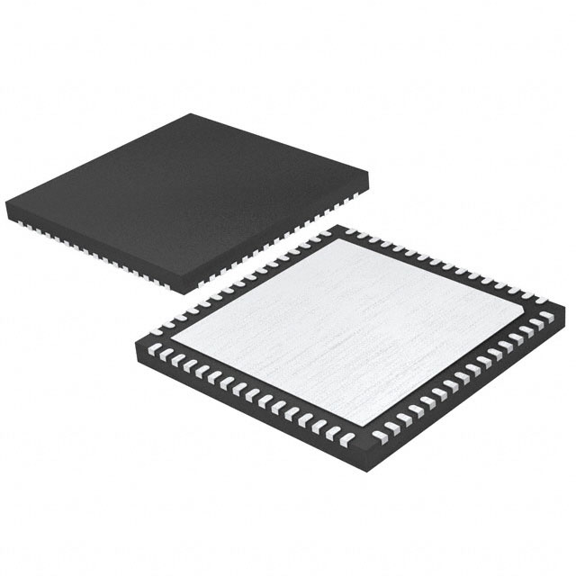


 工商网监
湘ICP备2023018690号
工商网监
湘ICP备2023018690号
