LTC3101
Wide VIN, Multi-Output
DC/DC Converter and
PowerPath Controller
DESCRIPTION
FEATURES
n
n
n
n
n
n
n
n
n
n
n
n
The LTC®3101 is a complete power management solution
for low power portable devices. It provides three high
efficiency switching DC/DC converters which seamlessly
transition from battery to USB/wall adapter power when
available. A synchronous buck-boost regulator provides
complete flexibility, allowing operation from a single
Li-Ion/Polymer battery, 2 to 3 AA cells, a USB port or any
other power source operating from 1.8V to 5.5V.
Low Loss PowerPath™ Control: Seamless,
Automatic Transition from Battery to USB or
Wall Adapter Power
Wide VIN Range: 1.8V to 5.5V
Buck-Boost VOUT: 1.5V to 5.25V
Buck-Boost Generates 3.3V at 300mA for
VIN ≥ 1.8V, 3.3V at 800mA for VIN ≥ 3V
Dual 350mA Buck Regulators, VOUT: 0.6V to VIN
38μA Quiescent Current in Burst Mode® Operation
1.8V, 50mA Always-On LDO
Protected 100mA Hot Swap™ Output
Pushbutton On/Off Control
Current Limited 200mA MAX Output
Programmable Power-Up Sequencing
24-lead 4mm × 4mm × 0.75mm QFN Package
Two always-alive outputs, a 50mA LDO and a 200mA MAX
output that tracks the higher voltage input supply, provide
power for critical functions or additional external regulators. Flash memory cards can be directly powered from
the protected 100mA Hot Swap output. Pushbutton control
logic and a programmable-duration microprocessor reset
generator simplify interfacing to a microprocessor while
internal sequencing and independent enable pins provide
flexible power-up options. The LTC3101 is available in a low
profile (0.75mm) 24-lead 4mm × 4mm QFN package.
APPLICATIONS
n
n
n
Ultra-Portable Digital Video Cameras
Personal Handheld GPS Navigators
Portable Medical Instruments
L, LT, LTC, LTM, Burst Mode, Linear Technology and the Linear logo are registered trademarks
and Hot Swap and PowerPath are trademarks of Linear Technology Corporation. All other
trademarks are the property of their respective owners.
TYPICAL APPLICATION
10μF
CELLS
USB/WALL
ADAPTER
4.3V TO 5.5V
10μF
10μF
4.7μH
BAT1 BAT2 SW3A
USB1
USB2
CRS
SW3B OUT3
FB3
HSO
MAX
LDO
0.1μF
DIS ENA
ENA1
ENA2
ENA3
SW2
LTC3101
ON/OFF
96
Hot Swap OUTPUT: 3.3V AT 100mA
TRACKING OUTPUT: 200mA
1.8V AT 50mA
4.7μF
4.7μH
VOUT2
1.8V
10μF 350mA
221k
110k
SW1
10μF
221k
FB1
GND
BUCK-BOOST
IOUT = 150mA
94
92
BUCK2
IOUT = 150mA
90
BUCK1
IOUT = 150mA
88
86
4.7μH
PBSTAT
PWM
PWRON
RESET
Efficiency vs VBAT
221k
FB2
PWRKEY
μP
1M
VOUT3 = 3.3V
300mA FOR VIN ≥ 1.8V
800mA FOR VIN ≥ 3V
EFFICIENCY (%)
+
2 AA
147k
VOUT1
1.5V
350mA
84
1.5
2.5
3.5
VBAT (V)
4.5
5.5
3101 TA01b
3101 TA01a
3101fb
1
�LTC3101
ABSOLUTE MAXIMUM RATINGS
PIN CONFIGURATION
(Note 1)
ENA3
SW3B
ENA1
FB2
FB1
ENA2
TOP VIEW
24 23 22 21 20 19
PWM 1
18 HSO
SW1 2
17 OUT3
BAT1 3
16 USB2
25
GND
USB1 4
15 SW3A
SW2 5
14 BAT2
13 RESET
PBSTAT
CRS
9 10 11 12
MAX
8
LDO
7
FB3
PWRON 6
PWRKEY
VBAT1, VBAT2, VUSB1, VUSB2 ......................... –0.3V to 6V
VSW1, VSW2, VSW3A, VSW3B
DC............................................................ –0.3V to 6V
Pulsed (400mA), it
is recommended that a 22μF or larger output capacitor be
used. The capacitor should be placed as close to the IC as
possible and should have a short return path to ground.
ENA3 (Pin 19): Enable Pin for Buck-Boost Converter.
Forcing this pin above 1V will turn on the buck-boost
converter when the IC is enabled (via the pushbutton
interface). Forcing this pin below 0.3V will disable the
buck-boost converter.
SW3B (Pin 20): Buck-Boost Switch Pin. This pin should
be connected to one side of the buck-boost inductor.
ENA1 (Pin 21): Enable Pin for Buck Converter 1. Forcing
this pin above 1V will turn on the buck converter when the
IC is enabled (via the pushbutton interface). Forcing this
pin below 0.3V will disable buck converter 1.
FB2 (Pin 22): Feedback Voltage Input for Buck Converter 2.
The resistor divider connected to this pin sets the output
voltage for buck converter 2.
FB1 (Pin 23): Feedback Voltage Input for Buck Converter 1.
The resistor divider connected to this pin sets the output
voltage for buck converter 1.
ENA2 (Pin 24): Enable Pin for Buck Converter 2. Forcing
this pin above 1V will turn on the buck converter when the
IC is enabled (via the pushbutton interface). Forcing this
pin below 0.3V will disable buck converter 2.
GND (Exposed Pad Pin 25): Small-Signal and Power
Ground for the IC. The Exposed Pad must be soldered to
the PCB and electrically connected to ground through the
shortest and lowest impedance connection possible.
HSO (Pin 18): Hot Swap Output. An internal current-limited
switch connects the HSO output to the buck-boost output
voltage after the buck-boost output reaches regulation.
With the buck-boost operating in PWM mode, this output
is guaranteed to support a 100mA load and is short-circuit
protected.
3101fb
11
�LTC3101
BLOCK DIAGRAM
14
16
BAT2*
15
USB2*
20
SW3A
17
SW3B
OUT3
WELL
CONTROL
MAX
CONTROL
AND
CURRENT
LIMIT
D
HSO
18
A
11
MAX
B
A´
10
3
4
C
Hot Swap
CONTROL
ALWAYS-ON
LDO
CONTROL
LDO
BAT1*
FB3
BUCK-BOOST
CONTROL
USB1*
ENA3
4M
WELL
CONTROL
7
19
VCC
400k
2
SW1
1.27MHz
OSCILLATOR
BANDGAP
REFERENCE
OVERTEMPERATURE
SHUTDOWN AND
UNDERVOLTAGE
LOCKOUT
BUCK 1
CONTROL
23
21
24ms
DEGLITCH
FB1
ENA1
PBSTAT
8
9
PUSHBUTTON
CONTROL
LOGIC
PWM
PWRON
1
6
4M
4M
RESET
WELL
CONTROL
5
PWRKEY
1μA
SW2
1.20V
+
–
CRS
13
12
DISABLED
FB1 POWER BAD (IF ENABLED)
FB2 POWER BAD (IF ENABLED)
FB3 POWER BAD (IF ENABLED)
UNDERVOLTAGE FAULT
OVERTEMPERATURE FAULT
BUCK 2
CONTROL
4M
24
22
ENA2
FB2
GND
(EXPOSED PAD)
25
*BAT1 AND BAT2 MUST BE CONNECTED TOGETHER IN THE APPLICATION
USB1 AND USB2 MUST BE CONNECTED TOGETHER IN THE APPLICATION
3101 BD
3101fb
12
�LTC3101
OPERATION
INTRODUCTION
The LTC3101 provides a complete power management
solution for low power portable devices. It generates a
total of six output voltage rails and provides a seamless,
automatic transition between two input power sources.
The LTC3101 contains three high efficiency synchronous
DC/DC converters: a 5-switch buck-boost DC/DC converter and two synchronous 3-switch step-down DC/DC
converters. The buck-boost DC/DC converter is typically
utilized to provide a 3V or 3.3V rail that lies within the
input voltage range. The two step-down converters can
be configured to provide two lower voltage output rails,
such as a 1.8V rail for SDRAM and a 1.2V rail to supply
the system microprocessor.
The LTC3101 can operate from any power source over the
wide input voltage range of 1.8V to 5.5V. All three switching
DC/DC converters operate from a common 1.27MHz oscillator and a single pin can be used to place all three DC/DC
converters into Burst Mode operation to reduce the total
no-load quiescent current with all six output voltage rails
active to only 38μA (typical). In standby operation, with
only the LDO and MAX outputs active, the input current
is reduced to 15μA (typical).
The 5-switch buck-boost DC/DC converter generates a
user-programmable output voltage rail that can lie within
the voltage range of the input power sources. Utilizing
a proprietary switching algorithm, the buck-boost converter maintains high efficiency and low noise operation
with input voltages that are above, below, or even equal
to the required output rail. A protected Hot Swap output
powered by the buck-boost output voltage rail is enabled
once the buck-boost reaches regulation. This provides a
current-limited output that can be shorted without affecting
the primary buck-boost output. One use of the Hot Swap
output is to power external flash memory cards that need
to be hot-plugged without disrupting the primary buckboost output rail.
The synchronous buck converters are typically used to
provide two high efficiency lower voltage rails and support 100% duty cycle operation to extend battery life. The
output voltage of each buck converter is independently
user programmable and can be set as low as 0.6V.
An always-alive LDO provides a fixed 1.8V output at 50mA
which can be utilized to power critical functions such as a
real time clock. Reverse blocking allows the LDO to be used
to charge a supercapacitor for memory retention when both
power sources are removed. The MAX output generates
a secondary always-alive, current-limited output rail that
tracks the higher voltage input power source (battery or
USB) and is convenient for powering additional external
LDOs and circuitry that can function directly from a wide
input voltage range.
A pushbutton interface and internal supply sequencing
complete the LTC3101 as a total power supply solution
while requiring only a minimal number of supporting
external components. Integral to the pushbutton control
is an internal microprocessor reset generator with a reset
duration that can be easily programmed using a single
external capacitor allowing the interface to be customized
to each particular application.
The extensive functionality and flexibility of the LTC3101,
along with its small size and high efficiency, make it an
excellent power solution for a wide variety of low power
portable electronic products.
PUSHBUTTON INTERFACE
The LTC3101 includes a pushbutton interface that allows
a single momentary pushbutton to control the sequenced
power-up and power-down of all output rails in coordination with an external microprocessor. In addition, three
independent enable pins allow an unused DC/DC converter
to be independently disabled and also provide the means
to manually implement an alternate power-up sequence.
The LTC3101 can be enabled by either forcing PWRON
high or by forcing PWRKEY low. In either case, the DC/DC
converters (if enabled by their respective enable pin)
will power up in the internally fixed default sequence:
buck converter 1, buck converter 2, and finally the buckboost converter. In the typical application, the power-on
sequence is initiated when the PWRKEY is driven low by an
external momentary pushbutton. Once the microprocessor is powered up it must assert PWRON high before the
pushbutton is released, thereby forcing the LTC3101 to
3101fb
13
�LTC3101
OPERATION
remain enabled. Power-down is usually accomplished by
having the microprocessor monitor PBSTAT to detect an
additional push of the pushbutton. Once this is detected,
the microprocessor disables the LTC3101 by forcing
PWRON low (or simply releasing PWRON and allowing
it be pulled low by its internal pull-down resistor). In
this manner, a single external momentary pushbutton is
all that is required to provide sequenced power-up and
power-down control.
Figure 1 depicts the waveforms in the standard power-up
sequence. In this example, it is assumed that all three
DC/DC converter rails are used in the application and
therefore ENA1, ENA2 and ENA3 are driven high (or tied
to the MAX output). An external normally-open pushbutton
is connected between ground and the PWRKEY pin. When
the pushbutton is not pressed, PWRKEY is pulled high
via an internal 400k pull-up resistor. Until the power-up
sequence is initiated, the IC is in the standby state, and
only the LDO and MAX outputs are active.
The standard power-up sequence is initiated when
the pushbutton is pressed, forcing PWRKEY low for a
duration that is longer than the 24ms (typical) internal
debouncing duration. Once the PWRKEY is held low for
the debouncing duration, PBSTAT is driven low to indicate
the pushbutton status. In addition, buck converter 1 is
enabled and its output begins rising into regulation. Once
the feedback voltage of buck converter 1 reaches its power
good threshold, buck converter 2 is enabled. After buck
converter 2 reaches its power good threshold, the buckboost converter is enabled. Finally, once the buck-boost
output reaches its power good threshold, the Hot Swap
output is enabled and simultaneously the microprocessor
reset duration begins when a 1μA (nominal) current begins
charging the external CRS capacitor. The microprocessor
reset output, RESET, is driven low throughout this entire
power-up sequence until the CRS pin is charged to 1.2V
(typical). Once RESET goes high, the microprocessor in
the application initializes and must drive the PWRON input
of the LTC3101 high in order to keep the LTC3101 enabled.
If PWRON is not driven high by the time PWRKEY returns
high (i.e., the pushbutton is released) then the LTC3101
will be disabled and all outputs will be actively discharged
to ground.
PWRKEY
PBSTAT
24ms BLANKING
VOUT BUCK 1
VOUT BUCK 2
VOUT BUCK-BOOST
HSO
CRS
RESET
PWRON
3101 F01
Figure 1. Power-Up Sequence Waveforms
3101fb
14
�LTC3101
OPERATION
Independent Enables
Each of the buck converters and the buck-boost converter
have independent enable pins (ENA1, ENA2 and ENA3).
These provide an additional degree of flexibility by allowing any unused channels to be independently disabled
and skipped in the power-up sequence. For example, if
the additional low voltage rail generated by the second
buck converter is not required, it can be disabled by
simply forcing ENA2 to ground. The power-up sequence
will be unaffected except that second buck converter will
be skipped. As a result, buck converter 1 will power up
and the buck-boost will be enabled as soon as buck converter 1 reaches regulation. Any unused channels can be
disabled in this fashion and they will simply be skipped
in the power-up sequence.
Manual Power-Up Via The PWRON Pin
If the pushbutton interface is not required, the LTC3101
can be manually enabled by simply forcing the PWRON
pin high. When PWRON is forced high any channels that
are enabled via their independent enable pin will power
up in the standard sequence (buck converter 1, buck converter 2 and then the buck-boost converter). An arbitrary
power-up sequence can be forced manually, by forcing all
enables (ENA1, ENA2, ENA3) low while bringing PWRON
high. Then, after waiting 10μs for the logic to initialize,
the individual converters can be manually enabled via their
independent enable pins in any order required. For example,
a simultaneous power-up is initiated by bringing PWRON
high while holding ENA1, ENA2 and ENA3 low. Then after
a 10μs or longer delay, ENA1, ENA2 and ENA3 can be
brought high simultaneously causing the two buck rails
and the buck-boost rail to begin rising simultaneously.
Fault Conditions
On an overtemperature or input undervoltage fault condition, all DC/DC converters, the LDO, and the MAX output
are disabled and the CRS pin is driven low which results
in the microprocessor reset output, RESET, being driven
low as well. In the standard application, this will cause
the microprocessor to release the PWRON pin, thereby
disabling the LTC3101. Consequently, the LTC3101 will not
automatically re-enable even if the fault condition clears.
Instead, the LTC3101 will have to be restarted via repeating
the normal power-up sequence. Alternatively, if PWRON is
held high until the fault condition clears, then any enabled
converters will power up in the default sequence once the
fault clears and the microprocessor reset will clear after
its programmed delay.
If the power good comparator for any converter indicates a
fault condition (loss of regulation), the CRS pin and RESET
pins are driven low. In a typical application, this will place
the microprocessor in the reset condition which will release
the force on PWRON and therefore disable the LTC3101.
However, if PWRON is maintained high, all converters will
remain enabled through the fault condition. Once the fault
condition clears, the affected converter output will recover,
and CRS will begin charging. After the programmed reset
duration, RESET will be released.
LDO OUTPUT
The LDO output generates a regulated 1.8V (nominal)
output voltage rail that is guaranteed to support a 50mA
load. The LDO output remains active whenever a valid
supply is present on either the USB2 or BAT2 inputs and
is unaffected by the pushbutton interface. Its always-on
status allows the LDO to power critical functions such as
a real time clock which must remain powered under all
conditions.
The LDO output is reverse blocking in shutdown (i.e.,
when undervoltage lockout threshold is reached) allowing
its output to stay charged when both input supplies are
removed with reverse leakage guaranteed to be under 1μA.
This allows the LDO to be used to charge a supercapacitor for memory retention purposes or powering standby
functions during times when both power sources are
removed. The LDO is specifically designed to be stable
with a small 4.7μF capacitor, but to also maintain stable
operation with arbitrarily large capacitance supercapacitors
without requiring a series isolation resistor.
The LDO output is current-limit protected. On an
undervoltage or overtemperature fault, the LDO is disabled
until the fault condition clears.
3101fb
15
�LTC3101
OPERATION
MAX OUTPUT
The MAX output generates a protected output rail that tracks
the higher of the two input supplies, BAT2 or USB2. The
MAX output is current-limit protected and is guaranteed
to support a 200mA load.
The MAX output is an always-alive output, meaning it is
always enabled independent of the state of the pushbutton
interface. This allows the MAX output to power additional
LDOs or critical circuitry that must remain powered in
standby. In addition, the MAX output can be used to
efficiently power additional application circuits that can
operate directly from a wide input voltage range without
burdening one of the switching converters. The MAX output
is also a convenient supply for forcing logic inputs (such
as PWM, ENA1, ENA2 and ENA3) high since it is powered
whenever either input supply is present.
The MAX output is disabled in undervoltage lockout and
during overtemperature shutdown. Since the MAX output
serves as the input to the LDO, it is recommended that
it be bypassed with a 1μF or greater ceramic capacitor if
the LDO is to be used in the application.
Hot Swap (HSO) OUTPUT
The HSO output is generated by a protected power switch
from the output of the buck-boost converter. It provides
a current-limited output that can be shorted to ground
without disrupting the buck-boost output voltage. This
is primarily intended to be used as a supply rail for flash
memory cards which can be hot-plugged in the application. When a card is hot-plugged into the HSO output,
the supply bypass capacitors on the card are gradually
charged via the current-limited output without affecting
the buck-boost output rail. The HSO output is not enabled
until the buck-boost is enabled and the buck-boost power
good comparator indicates it is in regulation.
BUCK CONVERTER OPERATION
The LTC3101 contains two independent buck DC/DC
converters each capable of supplying a 350mA load. Each
has an adjustable output voltage that can be set as low as
0.6V. In addition, each buck converter supports low dropout operation to extend battery life. These converters can
be utilized in Burst Mode operation to improve light-load
efficiency and no-load standby current or in PWM mode
to ensure low noise operation. Each buck converter has
dual P-channel power switches and a single N-channel
synchronous rectifier. The dual P-channel power switches
allow the buck converters to operate directly from either
the battery or USB inputs (BAT1 or USB1). The buck
converters will automatically and seamlessly transition
to operate from the higher voltage supply. Both buck
converters feature short-circuit protection and frequency
foldback to prevent inductor current run-away during low
resistance output short conditions.
PWM Mode Operation
If the PWM pin is forced high, both buck converters will
operate in fixed frequency pulse width modulation mode
using current mode control. At the start of each oscillator
cycle, the active P-channel switch is turned on and remains
on until the inductor current with superimposed slope
compensation ramp exceeds the error amplifier output.
At this point, the synchronous rectifier is turned on and
remains on until the inductor current falls to zero or a new
switching cycle is initiated. As a result, the buck converter
operates with discontinuous inductor current at light loads
in order to improve efficiency. At extremely light loads, the
minimum on-time of the P-channel switch will be reached
and the buck converter will begin turning off for multiple
cycles in order to maintain regulation.
Burst Mode Operation
When the PWM pin is forced low, both buck converters
will automatically and independently transition between
Burst Mode operation at sufficiently light loads (below
approximately 10mA) and PWM mode at heavier loads.
Burst Mode entry is determined by the peak inductor current and therefore the load current at which Burst Mode
operation will be entered depends on the input voltage,
the output voltage and the inductor value. Typical curves
for Burst Mode entry threshold are provided in the Typical
Performance Characteristics section of this data sheet.
In dropout operation, the active P-channel switch will
remain on continuously and Burst Mode operation will
not be entered.
3101fb
16
�LTC3101
OPERATION
Low Dropout Operation
Internal Voltage Mode Soft-Start
As the input voltage decreases to a value approaching
the output regulation voltage, the duty cycle increases to
the maximum on-time of the P-channel switch. Further
reduction of the supply voltage will force the main switch
to remain on for more than one cycle and subharmonic
switching will occur to provide a higher effective duty cycle.
If the input voltage is decreased further, the buck converter
will enter 100% duty cycle operation and the P-channel
switch will remain on continuously. In this dropout state,
the output voltage is determined by the input voltage less
the resistive voltage drop across the P-channel switch and
series resistance of the inductor.
Each buck converter has an independent internal voltage
mode soft-start circuit with a nominal duration of 800μs.
The buck converters remain in regulation during soft-start
and will therefore respond to output load transients which
occur during this time. In addition, the output voltage risetime has minimal dependency on the size of the output
capacitor or load current during start-up.
Slope Compensation
Current mode control requires the use of slope compensation to prevent sub-harmonic oscillations in the inductor
current waveform at high duty cycle operation. This function
is performed internally on the LTC3101 through the addition
of a compensating ramp to the current sense signal. In
some current mode ICs, current limiting is performed by
clamping the error amplifier voltage to a fixed maximum.
This leads to a reduced output current capability at low
step-down ratios. In contrast, the LTC3101 performs current-limiting prior to addition of the slope compensation
ramp and therefore achieves a peak inductor current limit
that is independent of duty cycle.
Output Short-Circuit Operation
When the output is shorted to ground, the error amplifier
will saturate high and the P-channel switch will turn on
at the start of each cycle and remain on until the current
limit trips. During this minimum on-time of the P-channel
switch, the inductor current will increase rapidly but will
decrease very slowly during the remainder of the period
due to the very small reverse voltage produced by a hard
output short. To eliminate the possibility of inductor current
runaway in this situation, the switching frequency of the
buck converters is reduced by a factor of four when the
voltage on the respective feedback pin (FB1 or FB2) falls
below 0.3V. This provides additional time for the inductor
current to reset and thereby protects against a build-up
of current in the inductor.
Error Amplifier and Internal Compensation
The LTC3101 buck converters utilize internal transconductance error amplifiers. Compensation of the buck converter
feedback loops is performed internally to reduce the size
of the application circuit and simplify the design process.
The compensation network has been designed to allow use
of a wide range of output capacitors while simultaneously
ensuring a rapid response to load transients.
Power Good Comparator Operation
Each buck converter has an internal power good comparator that monitors the respective feedback pin voltage (FB1
or FB2). The power good comparator outputs are used at
power-up for sequencing purposes. During normal operation, the power good comparators are used to monitor
the output rails for a fault condition. If either buck power
good comparator indicates a fault condition, the CRS and
RESET pins are driven low. This can be used to reset a
microprocessor in the application circuit when either buck
converter output rail loses regulation.
The buck power good comparator will trip when the
respective feedback pin falls 8% (nominally) below the
regulation voltage. With a rising output voltage, the power
good comparator will typically clear when the respective
feedback voltage rises to within 5.5% of the regulation
voltage. In addition, there is a 60μs typical deglitching
delay in the power good comparators in order to prevent
false trips due to brief voltage transients occurring on
load steps.
3101fb
17
�LTC3101
OPERATION
BUCK-BOOST CONVERTER OPERATION
The buck-boost converter is a synchronous 5-switch
DC/DC converter with the capability to operate efficiently
with input voltages that are above, below or equal to
the output regulation voltage. A proprietary switching
algorithm provides a smooth transition between operational modes while maintaining high efficiency and low
noise performance. Referring to the Block Diagram, the
buck-boost converter has two P-channel input power
switches, A and A´. This provides the capability for the
buck-boost converter to operate directly from either input
power source, USB or battery. The buck-boost converter
automatically and seamlessly transitions to the higher
voltage input supply.
PWM Mode Operation
When the PWM pin is held high, the LTC3101 buck-boost
converter operates in a fixed frequency pulse width modulation mode using voltage mode control. A proprietary
switching algorithm allows the converter to transition
between buck, buck-boost, and boost modes without
discontinuity in inductor current or loop characteristics.
The switch topology for the buck-boost converter is shown
in Figure 2.
When the input voltage is significantly greater than the
output voltage, the buck-boost converter operates in
buck mode. Switch D turns on continuously and switch
C remains off. Switches A (or A´) and B are pulse width
modulated to produce the required duty cycle to support the
output regulation voltage. As the input voltage decreases,
switch A remains on for a larger portion of the switching
cycle. When the duty cycle reaches approximately 85%,
the switch pair AC begins turning on for a small fraction
of the switching period. As the input voltage decreases
further, the AC switch pair remains on for longer durations
and the duration of the BD phase decreases proportionally.
As the input voltage drops below the output voltage, the
AC phase will eventually increase to the point that there is
no longer any BD phase. At this point, switch A remains on
continuously while switch pair CD is pulse width modulated to obtain the desired output voltage. At this point,
the converter is operating solely in boost mode.
This switching algorithm provides a seamless transition
between operating modes and eliminates discontinuities
in average inductor current, inductor current ripple, and
loop transfer function throughout all three operational
modes. These advantages result in increased efficiency
and stability in comparison to the traditional 4-switch
buck-boost converter.
Error Amplifier and Internal Compensation
The buck-boost converter utilizes a voltage mode error
amplifier with an internal compensation network as shown
in Figure 3.
Notice that resistor R2 of the external resistor divider
network plays an integral role in determining the frequency
response of the compensation network. The ratio of R2 to
R1 is set to program the desired output voltage but this
still allows the value of R2 to be adjusted to optimize the
LTC3101
VOUT3
L
USB2 BAT2
A´
SW3A
SW3B
D
VOUT3
VOUT3
R2
+
–
0.599V
FB3
A
R1
B
C
GND (EXPOSED PAD)
LTC3101
3101 F02
Figure 2. Buck-Boost Switch Topology
Figure 3. Buck-Boost Error Amplifier and Compensation
3101fb
18
�LTC3101
OPERATION
transient response of the converter. Increasing the value
of R2 generally leads to greater stability at the expense of
reduced transient response speed. Increasing the value of
R2 can yield substantial transient response improvement
in cases where the phase margin has been reduced due to
use of a small value output capacitor or a large inductance
(particularly with large boost step-up ratios). Conversely,
decreasing the value of R2 increases the loop bandwidth
which can improve the speed of the converter’s transient
response. This can be useful in improving the transient
response if a large value output capacitor is utilized. In
this case, the increased bandwidth created by decreasing
R2 is used to counteract the reduced converter bandwidth
caused by the large output capacitor.
Current Limit Operation
The buck-boost converter has two current limit circuits.
The primary current limit is an average current limit circuit which injects an amount of current into the feedback
node which is proportional to the extent that the switch A
(or A´) current exceeds the current limit value. Due to the
high gain of the feedback loop, the injected current forces
the error amplifier output to decrease until the average
current through switch A decreases approximately to the
current limit value. The average current limit utilizes the
error amplifier in an active state and thereby provides a
smooth recovery with little overshoot once the current limit
fault condition is removed. Since the current limit is based
on the average current through switch A (or A´), the peak
inductor current in current limit will have a dependency
on the duty cycle (i.e., on the input and output voltages)
in the overcurrent condition.
The speed of the average current limit circuit is limited by
the dynamics of the error amplifier. On a hard output short,
it would be possible for the inductor current to increase substantially beyond current limit before the average current
limit circuit would react. For this reason, there is a second
current limit circuit which turns off switch A (and A´) if the
current ever exceeds approximately 165% of the average
current limit value. This provides additional protection in
the case of an instantaneous hard output short.
Reverse Current Limit
A reverse current comparator on switch D monitors the
current entering the OUT3 pin. When this current exceeds
400mA (typical) switch D will be turned off for the remainder of the switching cycle. This feature protects the
buck-boost converter from excessive reverse current if the
buck-boost output is held above the regulation voltage by
an external source.
Burst Mode Operation
With the PWM pin held low, the buck-boost converter
operates utilizing a variable frequency switching algorithm
designed to improve efficiency at light load and reduce
the standby current at zero load. In Burst Mode operation,
the inductor is charged with fixed peak amplitude current
pulses. These current pulses are repeated as often as
necessary to maintain the output regulation voltage. The
maximum output current, IMAX, which can be supplied in
Burst Mode operation is dependent upon the input and
output voltage as given by the following formula:
IMAX =
0.15 • VIN
A
VIN + VOUT
( )
If the buck-boost load exceeds the maximum Burst Mode
current capability, the output rail will lose regulation and the
power good comparator will indicate a fault condition.
In Burst Mode operation, the error amplifier is not used but
is instead placed in a low current standby mode to reduce
supply current and improve light load efficiency.
Internal Voltage Mode Soft-Start
The buck-boost converter has an internal voltage mode
soft-start circuit with a nominal duration of 800μs. The
converter remains in regulation during soft-start and will
therefore respond to output load transients that occur
during this time. In addition, the output voltage rise time
has minimal dependency on the size of the output capacitor or load. During soft-start, the buck-boost converter is
forced into PWM mode operation regardless of the state
of the PWM pin.
3101fb
19
�LTC3101
OPERATION
Power Good Comparator Operation
The buck-boost converter contains an internal power
good comparator that continuously monitors the voltage
of the feedback pin FB3. The output of this comparator
is used during power-up for sequencing purposes. In addition, during operation, if the power good comparator
indicates a fault condition, CRS and RESET will be driven
low. This feature can be used to reset a microprocessor
in the application circuit if the buck-boost output loses
regulation.
In Burst Mode operation (PWM = low), the buck-boost
power good comparator will indicate a fault when the
feedback voltage falls approximately 8.5% below the regulation voltage. There is approximately 2.5% hysteresis in
this threshold when the output voltage is returning good.
In addition, there is a 60μs typical deglitching delay in
order to prevent false trips due to short duration voltage
transients in response to load steps.
In PWM mode, operation of the power good comparator
is complicated by the fact that the feedback pin voltage
is driven to the reference voltage independent of the
output voltage through the action of the voltage mode
error amplifier. Since the soft-start is voltage mode, the
feedback voltage will track the output voltage correctly
during soft-start, and the power good comparator output
will correctly indicate the point at which the buck-boost
attains regulation at the end of soft-start. However, once
in regulation, the feedback voltage will no longer track the
output voltage and the power good comparator will not
immediately respond to a loss of regulation in the output.
For this reason, the power good comparator output is also
designed to indicate a fault condition if the buck-boost
converter enters current limit. The only means by which a
loss of regulation can occur is if the current limit has been
reached thereby preventing the buck-boost converter from
delivering the required output current. In such cases, the
occurrence of current limit will directly cause the power
good comparator to indicate a fault state. However, there
may be cases at the boundary of reaching current limit
when the buck-boost converter is continuously in current
limit, causing the power good comparator to indicate a
fault, but the output voltage may be slightly above the
actual power good threshold.
COMMON FUNCTIONS
Thermal Shutdown
If the die temperature exceeds 150°C all DC/DC converters
will be disabled. In addition, the LDO and MAX outputs are
disabled. All power devices are turned off and all switch
nodes will be high impedance. The soft-start circuits for all
converters are reset during thermal shutdown to provide
a smooth recovery once the overtemperature condition is
eliminated. All DC/DC converters (if enabled) and the LDO
and MAX outputs will restart when the die temperature
drops to approximately 140°C.
Undervoltage Lockout
If the supply voltage decreases below 1.65V (typical) then
all DC/DC converters will be disabled and all power devices
are turned off. In addition, the MAX and LDO outputs are
disabled. The LDO is forced into its reverse blocking state,
allowing the LDO output to remain powered with less
than 1μA reverse current being drawn by the LTC3101.
The soft-start circuits for all DC/DC converters are reset
during undervoltage lockout to provide a smooth restart
once the input voltage rises above the undervoltage
lockout threshold.
Active Output Discharge
All three DC/DC converter outputs are actively discharged
to ground when disabled through 1kΩ (typical) impedances. The buck converter outputs are discharged through
the inductor via a pull-down resistor on the respective
switch pin.
3101fb
20
�LTC3101
APPLICATIONS INFORMATION
The basic LTC3101 application circuit is shown as the
Typical Application on the front page of this data sheet.
The external component selection is dependent upon the
required performance of the IC in each particular application given considerations and tradeoffs such as PCB
area, output voltages, output currents, ripple voltages
and efficiency. This section of the data sheet provides
some basic guidelines and considerations to aid in the
selection of external components and the design of the
application circuit.
CRS Capacitor Selection
A capacitor from the CRS pin to ground is used to program the duration of the microprocessor reset signal on
the RESET pin. A low leakage ceramic capacitor should
be utilized to ensure reliable temperature independent
operation. At the start of the active-low reset pulse, a 1μA
(typical) current begins charging the CRS capacitor. The
RESET pulse ends when the voltage at the CRS pin reaches
1.20V (typical). Therefore, the required CRS capacitor value,
CRS, is given by the following equation where tRESET is the
desired reset duration in milliseconds:
CRS =
tRESET
μF
1200
( )
If the microprocessor reset function of the LTC3101 is
unused, the CRS pin can be left unconnected.
LDO Output Capacitance
The LDO has been specifically designed for stable operation with a wide range of output capacitors. For most applications, a low ESR ceramic capacitor of at least 4.7μF
should be utilized. Large valued supercapacitors can be
connected directly to the LDO output without requiring a
series isolation resistor for loop stability. However, if the
supercapacitor has significant ESR, it may be necessary
to place a small 4.7μF ceramic in parallel with the supercapacitor to maintain an adequate phase margin.
MAX Capacitor Selection
The MAX output serves as the input to the LDO. Therefore, even if the MAX output is unused directly in the
application, it is recommended that it be bypassed with
a 1μF or larger ceramic capacitor. There is no limit to the
maximum capacitance on this pin. However, the soft-start
duration is formed by the current-limited output charging the capacitance attached to the pin so larger output
capacitors will result in proportionally longer soft-start
durations.
Buck Inductor Selection
The choice of buck inductor value influences both the efficiency and the magnitude of the output voltage ripple.
Larger inductance values will reduce inductor current
ripple and will therefore lead to lower output voltage
ripple. For a fixed DC resistance, a larger value inductor
will yield higher efficiency by lowering the peak current to
be closer to the average output current. However, a larger
inductor within a given inductor family will generally have
a greater series resistance, thereby counteracting this
efficiency advantage.
Given a desired peak-to-peak current ripple, ΔIL, the
required inductance can be calculated via the following
expression, where f represents the switching frequency
in MHz:
L=
VOUT � VOUT �
�1–
� (μH)
f • �IL �
VIN �
A reasonable choice for ripple current is ΔIL = 140mA
which represents 40% of the maximum 350mA load
current. The DC current rating of the inductor should be
at least equal to the maximum load current plus half the
ripple current in order to prevent core saturation and loss
of efficiency during operation. To optimize efficiency the
inductor should have a low DC resistance (DCR).
In particularly space-restricted applications it may be
advantageous to use a much smaller value inductor at
the expense of larger ripple current. In such cases, the
converter will operate in discontinuous conduction for a
wider range of output loads and efficiency will be reduced.
In addition, there is a minimum inductor value required
to maintain stability of the current loop as determined by
the fixed internal slope compensation. Specifically, if the
3101fb
21
�LTC3101
APPLICATIONS INFORMATION
buck converter is going to be utilized at duty cycles over
40%, the inductance value must be at least equal to LMIN
as given by the following equation:
Table 2. Representative Buck Inductors
VALUE
(μH)
DCR
(Ω)
MAX DC
CURRENT (A)
SIZE (mm)
W×L×H
Coilcraft
LPS3015
EPL2014
EPL2010
LPS4018
4.7
4.7
4.7
4.7
0.20
0.23
0.43
0.125
1.2
0.88
0.65
1.9
3.0 × 3.0 × 1.5
2.0 × 2.0 × 1.4
2.0 × 2.0 × 1.0
4.0 × 4.0 × 1.8
Cooper-Bussmann
SD3118
SD3112
SD3110
SD10
4.7
4.7
4.7
4.7
0.162
0.246
0.285
0.154
1.31
0.80
0.68
1.08
3.1 × 3.1 × 1.8
3.1 × 3.1 × 1.2
3.1 × 3.1 × 1.0
5.2 × 5.2 × 1.0
Murata
LQH3NP
LQM31PN
LQH32CN
4.7
4.7
4.7
0.26
0.30
0.15
0.80
0.70
0.65
3.0 × 3.0 × 0.9
3.2 × 1.6 × 0.85
3.2 × 2.5 × 2.0
Panasonic
ELLVEG
ELL4G
ELL4LG
4.7
4.7
4.7
0.24
0.16
0.09
0.70
0.86
1.10
3.0 × 3.0 × 1.0
3.8 × 3.8 × 1.1
3.8 × 3.8 × 1.8
Sumida
CDRH2D09
CDRH3D16/LD
CDRH2D09B
4.7
4.7
4.7
0.167
0.081
0.218
0.42
0.62
0.70
3.2 × 3.2 × 1.0
3.2 × 3.2 × 1.8
3.0 × 2.8 × 1.0
Taiyo-Yuden
CBC2518
CBC3225T
NR3010T
4.7
4.7
4.7
0.2
0.1
0.19
0.68
1.01
0.75
2.5 × 1.8 × 1.8
3.2 × 2.5 × 2.5
3.0 × 3.0 × 1.0
TOKO
DE2812C
D310F
DB3015C
4.7
4.7
4.7
0.13
0.26
0.09
1.2
0.9
0.86
3.0 × 3.2 × 1.2
3.8 × 3.8 × 1.0
3.2 × 3.2 × 1.8
Buck Output Capacitor Selection
Wurth
744028004
744032004
744029003
4.7
4.7
4.7
0.265
0.280
0.170
0.90
0.49
0.80
2.8 × 2.8 × 1.1
3.2 × 2.5 × 2.0
2.8 × 2.8 × 1.35
A low ESR output capacitor should be utilized at the buck
converter output in order to minimize output voltage ripple.
Multilayer ceramic capacitors are an excellent choice as
they have low ESR and are available in small footprints. In
addition to controlling the ripple magnitude, the value of
the output capacitor also sets the loop crossover frequency
and therefore can impact loop stability. In general, there is
both a minimum and maximum capacitance value required
to ensure stability of the loop. If the output capacitance is
too small, the loop crossover frequency will increase to
the point where switching delay and the high frequency
parasitic poles of the error amplifier will degrade the phase
margin. In addition, the wider bandwidth produced by a
small output capacitor will make the loop more susceptible
to switching noise. Table 3 depicts the minimum recommended output capacitance for several typical output
voltages. At the other extreme, if the output capacitor is
too large, the crossover frequency can decrease too far
below the compensation zero and also lead to degraded
phase margin. In such cases, the phase margin and transient performance can be improved by simply increasing
the size of the feedforward capacitor in parallel with the
upper resistor divider resistor. (See Buck Output Voltage
Programming section for more details).
LMIN = 2.5 • VOUT (μH)
Table 1 depicts the minimum required inductance for
several common output voltages.
Table 1. Buck Minimum Inductance
OUTPUT VOLTAGE
MINIMUM INDUCTANCE
0.8V
2.0μH
1.2V
3.0μH
1.8V
4.7μH
2.0V
5.0μH
2.7V
6.8μH
A large variety of low ESR, high current power inductors
are available that are well suited to LTC3101 buck converter
applications. The tradeoff generally involves PCB area,
application height, required output current and efficiency.
Table 2 provides a representative sampling of small surface mount inductors that are well suited for use with
the LTC3101 buck converters. All inductor specifications
are listed at an inductor value of 4.7μH for comparison
purposes but other values within these inductor families
are generally well suited to this application as well. Within
each family (i.e., at a fixed inductor size), the DC resistance
generally increases and the maximum current generally
decreases with increased inductance.
PART NUMBER
3101fb
22
�LTC3101
APPLICATIONS INFORMATION
capacitance of the feedback pin produce a parasitic pole
that can reduce the loop phase margin if it becomes too
low in frequency. For these reasons, it is recommended
that the resistance of R1 in parallel with R2 be kept under
300k. A reasonable compromise between noise immunity and quiescent current is provided by choosing R2 =
221k. The required value for R1 can then be calculated
via Equation 1.
Table 3. Buck Minimum Recommended Output Capacitance
OUTPUT VOLTAGE
MINIMUM RECOMMENDED
OUTPUT CAPACITANCE
0.6V
22μF
0.8V
22μF
1.2V
10μF
1.8V
10μF
2.7V
4.7μF
3.3V
4.7μF
Buck Input Capacitor Selection
The BAT1 and USB1 pins provides current to the power
stages of both buck converters. It is recommended that a
low ESR ceramic capacitor with a value of at least 4.7μF
be used to bypass each of these pins. These capacitors
should be placed as close to the respective pin as possible and should have a short return path to the backpad
of the IC.
Buck Output Voltage Programming
The buck output voltages are programmed via external
resistor dividers connected to the respective feedback pin
(FB1 or FB2) as shown in Figure 4.
The resistor divider resistors control the output voltage
according to the following formula:
� R2 �
VOUT1,2 = 0.596 �1+ � ( V )
� R1 �
(1)
If the impedance of the resistor divider is too high it will
increase noise sensitivity due to coupling of stray noise
to the feedback pin. In addition, the parallel resistance
of the resistor divider resistors in series with the input
VOUT1,2 ≥ 0.600V
R2
CFF
FB1,2
LTC3101
R1
GND
3101 F04
To further increase the noise immunity of the feedback pin
and improve the transient response of the buck converter,
a small value feedforward capacitor, CFF , can be added in
parallel with the upper feedback divider resistor, R2. This
reduces the impedance of the feedback pin at high frequencies thereby increasing its immunity from picking up stray
noise. In addition, this adds a pole-zero pair to the loop
dynamics which generates a phase boost that can improve
the phase margin and increase the speed of the transient
response, resulting in smaller voltage deviation on load
transients. The zero frequency depends not only on the
value of the feedforward capacitor, but also on the upper
resistor divider resistor. Specifically, the zero frequency,
fZERO, is given by the following equation:
fZERO =
1
2 • π • R2 • CFF
Ideally, the phase boost generated by the pole-zero pair
should be centered at the loop crossover frequency. Table 4
provides the recommended feedback divider resistor values
and corresponding feedforward capacitors for several
commonly utilized output voltages.
Table 4. Buck Resistor Divider and Feedforward Capacitor
Values
VOUT
R1
R2
CFF
COUT
0.6V
–
0
–
22μF
0.8V
649k
221k
18pF
22μF
1.0V
324k
221k
18pF
22μF
1.2V
221k
221k
18pF
10μF
1.5V
147k
221k
18pF
10μF
1.8V
110k
221k
18pF
10μF
2.0V
86.6k
205k
18pF
10μF
2.7V
56.2k
200k
18pF
4.7μF
3.3V
48.7k
221k
18pF
4.7μF
Figure 4. Setting the Buck Output Voltages
3101fb
23
�LTC3101
APPLICATIONS INFORMATION
If a substantially larger output capacitor is utilized, the
bandwidth of the loop will be reduced. In such cases, the
feedforward capacitor can be increased in value in order
to lower the zero frequency and improve the transient
response.
Buck-Boost Output Voltage Programming
The buck-boost output voltage is set via an external resistor
divider connected to the FB3 pin as shown in Figure 5.
buck-boost inductor must have a saturation current rating that is greater than the worst-case average inductor
current plus half the ripple current. The peak-to-peak
inductor current ripple will be larger in buck and boost
mode then in the buck-boost region. The peak-to-peak
inductor current ripple for each mode can be calculated
from the following formulas, where f is the frequency in
MHz and L is the inductance in μH:
�IL(P-P)(BUCK) =
5.25 ≥ VOUT3 ≥ 1.5V
VOUT � VIN – VOUT �
�
�
f •L �
VIN
�
R2
�IL(P-P)(BOOST) =
FB3
LTC3101
VIN � VOUT – VIN �
�
�
f • L � VOUT �
R1
GND
3101 F05
Figure 5. Setting the Buck-Boost Output Voltage
The resistor divider values determine the buck-boost output
voltage according to the following formula:
� R2 �
VOUT3 = 0.599 �1+ � ( V )
� R1 �
(2)
The buck-boost converter utilizes voltage mode control
and in addition to setting the output voltage, the value of
R2 plays an integral role in the dynamics of the feedback
loop. In general, a larger value for R2 will increase stability
and reduce the speed of the transient response. A smaller
value of R2 will reduce stability but increase the speed of
the transient response. A good starting point is to choose
R2 = 1M and then calculate the required value of R1 to
set the desired output voltage according to Equation 2.
If a large output capacitor is used, the bandwidth of the
converter is reduced. In such cases R2 can be reduced
to improve the transient response. If a large inductor or
small output capacitor is utilized the loop will be less stable
and the phase margin can be improved by increasing the
value of R2.
Buck-Boost Inductor Selection
To achieve high efficiency, a low ESR inductor should
be utilized for the buck-boost converter. In addition, the
In addition to affecting output current ripple, the size of
the inductor can also impact the stability of the feedback
loop. In boost mode, the converter transfer function has
a right half plane zero at a frequency that is inversely
proportional to the value of the inductor. As a result, a
large inductor can move this zero to a frequency that is
low enough to degrade the phase margin of the feedback
loop. It is recommended that the inductor value be chosen
less than 10μH if the buck-boost converter is to be used
in the boost region.
In addition to affecting the efficiency of the buck-boost
converter, the inductor DC resistance can also impact the
maximum output capability of the buck-boost converter
at low input voltage. In buck mode, the buck-boost output
current is limited only by the inductor current reaching the
current limit value. However, in boost mode, especially at
large step-up ratios, the output current capability can also
be limited by the total resistive losses in the power stage.
These include switch resistances, inductor resistance,
and PCB trace resistance. Use of an inductor with high
DC resistance can degrade the output current capability
from that shown in the graph in the Typical Performance
Characteristics section of this data sheet.
Different inductor core materials and styles have an impact
on the size and price of an inductor at any given current
rating. Shielded construction is generally preferred as it
minimizes the chances of interference with other circuitry.
The choice of inductor style depends upon the price, sizing,
and EMI requirements of a particular application. Table 5
3101fb
24
�LTC3101
APPLICATIONS INFORMATION
provides a small sampling of inductors that are well suited
to many LTC3101 buck-boost converter applications. All
inductor specifications are listed at an inductance value
of 4.7μH for comparison purposes but other values within
these inductor families are generally well suited to this application. Within each family (i.e., at a fixed size), the DC
resistance generally increases and the maximum current
generally decreases with increased inductance.
Table 5. Representative Buck-Boost Surface Mount Inductors
VALUE
(μH)
DCR
(mΩ)
MAX DC
CURRENT (A)
SIZE (mm)
W×L×H
Coilcraft
LPS4018
LPS4012
ME3220
MSS5121
4.7
4.7
4.7
4.7
125
175
190
95
1.9
1.8
1.5
1.66
4.0 × 4.0 × 1.8
4.0 × 4.0 × 1.2
3.2 × 2.5 × 2.0
5.4 × 5.4 × 2.1
Cooper-Bussmann
SD12
SD14
4.7
4.5
118
94
1.29
1.74
5.2 × 5.2 × 1.2
5.2 × 5.2 × 1.4
Panasonic
ELL6PG
ELL5PS
4.7
4.7
58
61
1.5
1.5
6.0 × 6.0 × 2.0
5.0 × 5.0 × 1.85
Sumida
CDRH3D18
CDRH4D15/S
CDRH4D22/HP
4.7
4.7
4.7
86
103
66
1.35
1.4
2.2
4.0 × 4.0 × 2.0
4.7 × 4.7 × 1.7
5.0 × 5.0 × 2.4
Taiyo-Yuden
NR6020T
NP04SZB
4.7
4.7
58
75
2.0
1.8
6.0 × 6.0 × 2.0
5.0 × 5.0 × 2.0
TOKO
DE2815C
DP418C
DE4514C
4.7
4.7
4.7
100
50
100
1.3
1.50
1.9
3.0 × 2.8 × 1.5
4.2 × 4.2 × 1.8
4.7 × 4.9 × 1.4
Wurth
744042004
7447785004
7447745056
4.7
4.7
4.7
82
78
57
1.65
2.20
2.40
4.8 × 4.8 × 1.8
5.9 × 6.2 × 3.3
5.2 × 5.8 × 2.0
PART NUMBER
capacitance in μF, L is the inductance in μH, and ILOAD is
the output current in Amps.
ΔVP-P(BUCK) =
1
8 • L • COUT • f 2
ΔVP-P(BOOST) =
•
( VIN – VOUT ) VOUT
VIN
ILOAD ( VOUT – VIN )
COUT • VOUT • f
Given that the output current is discontinuous in boost
mode, the ripple in this mode will generally be much larger
than the magnitude of the ripple in buck mode. In addition to controlling the ripple magnitude, the value of the
output capacitor also affects the location of the resonant
frequency in the open-loop converter transfer function.
If the output capacitor is too small, the bandwidth of the
converter will extend high enough to degrade the phase
margin. To prevent this from happening, it is recommended
that a minimum value of 10μF be used for the buck-boost
output capacitor. If the required buck-boost load current
is greater than 400mA, it is recommended that the output
capacitor be increased to 22μF to improve output voltage
ripple and loop stability.
Buck-Boost Input Capacitor Selection
The supply current to the buck-boost converter is provided
by the USB2 and BAT2 pins. In addition, these pins provide
power to the internal circuitry of the LTC3101. It is recommended that a low ESR ceramic capacitor with a value of
at least 10μF be located as close to each of these pins as
possible. In addition, the return trace from each pin to the
ground plane should be made as short as possible.
Buck-Boost Output Capacitor Selection
Capacitor Vendor Information
A low ESR output capacitor should be utilized at the buckboost converter output in order to minimize output voltage ripple. Multilayer ceramic capacitors are an excellent
choice as they have low ESR and are available in small
footprints. The capacitor should be chosen large enough
to reduce the output voltage ripple to acceptable levels.
Neglecting the capacitor ESR and ESL, the peak-to-peak
output voltage ripple can be calculated by the following
formulas, where f is the frequency in MHz, COUT is the
Both the input bypass capacitors and DC/DC converter
output capacitors used with the LTC3101 must be low ESR
and designed to handle the large AC currents generated
by switching converters. This is important to maintain
proper functioning of the IC and to reduce output ripple.
Many modern low voltage ceramic capacitors experience
significant loss in capacitance from their rated value
with increased DC bias voltages. For example, it is not
uncommon for a small surface mount ceramic capacitor
3101fb
25
�LTC3101
APPLICATIONS INFORMATION
to lose 45% of its rated capacitance when operated near
its rated voltage. As a result, it is sometimes necessary to
use a larger value capacitance or a capacitor with a higher
voltage rating than required in order to actually realize
the intended capacitance at the full operating voltage. For
details, consult the capacitor vendor’s curve of capacitance
versus DC bias voltage.
The capacitors listed in Table 6 provide a sampling of small
surface mount ceramic capacitors that are well suited to
LTC3101 application circuits. All listed capacitors are either
X5R or X7R dielectric in order to ensure that capacitance
loss over temperature is minimized.
Table 6. Representative Bypass and Output Capacitors
VALUE
(μF)
VOLTAGE
(V)
SIZE (mm)
L × W × H (FOOTPRINT)
AVX
12106D475K
12104D106K
12106D106K
12106D226K
4.7
10
10
22
6.3
4
6.3
6.3
1.6 × 0.8 × 0.86 (0603)
1.6 × 0.8 × 1.02 (0603)
2.0 × 1.25 × 1.4 (0805)
2.0 × 1.25 × 1.4 (0805)
Kemet
C0603C475K9P
C0603C106K9P
C0805C476K9P
4.7
10
47
6.3
6.3
6.3
1.6 × 0.8 × 0.8 (0603)
1.6 × 0.8 × 0.8 (0603)
2.0 × 1.25 × 1.25 (0805)
Murata
GRM18
GRM21
GRM21
GRM21
4.7
4.7
10
22
6.3
10
10
6.3
1.6 × 0.8 × 0.8 (0603)
2.0 × 1.25 × 1.25 (0805)
2.0 × 1.25 × 1.25 (0805)
2.0 × 1.25 × 1.25 (0805)
Samsung
CL10A475KP5LNN
CL10A106KQ8NNN
CL21A226MQCLRN
CL21A476MQYNNN
4.7
10
22
47
10
6.3
6.3
6.3
1.6 × 0.8 × 0.55 (0603)
1.6 × 0.8 × 0.90 (0603)
2.0 × 1.25 × 0.95 (0805)
2.0 × 1.25 × 1.45 (0805)
Taiyo Yuden
JMK107BJ
LMK107BJ
JMK212BJ
JMK212BJ
10
4.7
22
47
6.3
10
6.3
6.3
1.6 × 0.8 × 0.8 (0603)
1.6 × 0.8 × 0.8 (0603)
2.0 × 1.25 × 0.85 (0805)
2.0 × 1.25 × 0.85 (0805)
TDK
C1608X5ROJ
C1608X5R0J
C1608X5R0J
C2012X5R0J
4.7
6.8
10
15
6.3
6.3
6.3
6.3
1.6 × 0.8 × 0.8 (0603)
1.6 × 0.8 × 0.8 (0603)
1.6 × 0.8 × 0.8 (0603)
2.0 × 1.25 × 0.85 (0805)
PART NUMBER
PCB Layout Considerations
The LTC3101 switches large currents at high frequencies.
Special attention should be paid to the PCB layout to ensure a stable, noise-free and efficient application circuit.
Figure 6 presents a representative PCB layout to outline
some of the primary considerations. A few key guidelines
are listed:
1. All circulating high current paths should be kept as
short as possible. This can be accomplished by keeping the routes to all components in Figure 6 as short
and as wide as possible. Capacitor ground connections
should via down to the ground plane in the shortest
route possible. The bypass capacitors on USB1, USB2,
BAT1 and BAT2 should be placed as close to the IC as
possible and should have the shortest possible paths
to ground.
2. The Exposed Pad is the small-signal and power ground
connection for the LTC3101. Multiple vias should connect the backpad directly to the ground plane. In addition maximization of the metallization connected to
the backpad will improve the thermal environment and
increase the power handling capabilities of the IC.
3. The components shown in bold and their connections
should all be placed over a complete ground plane to
minimize loop cross-sectional areas. This minimizes
EMI and reduces inductive drops.
4. Connections to all of the components shown in bold
should be made as wide as possible to reduce the series
resistance. This will improve efficiency and maximize the
output current capability of the buck-boost converter.
5. To prevent large circulating currents from disrupting
the output voltage sensing, the ground for each resistor
divider should be returned to the ground plane using
a via placed close to the IC and away from the power
connections.
6. Keep the connection from the resistor dividers to the
feedback pins FB1 and FB2 as short as possible and
away from the switch pin connections.
7. Crossover connections (such as the one shown from
SW3A to the inductor) should be made on inner copper
layers if available. If it is necessary to place these on
the ground plane, make the trace on the ground plane
as short as possible to minimize the disruption to the
ground plane.
3101fb
26
�VUSB
VBAT
VOUT2
INNER
COPPER
LAYER
INNER
COPPER
LAYER
(21)
ENA1
(10)
LDO
(22)
FB2
(9)
PBSTAT
(23)
FB1
(8)
PWRKEY
(24)
ENA2
(7)
FB3
(13)
RESET
(14)
BAT2
(15)
SW3A
(16)
USB2
(17)
OUT3
(18)
HSO
INNER
COPPER
LAYER
Figure 6. PCB Layout Recommendations
VIA TO GOUND PLANE
(AND TO INNER LAYER WHERE SHOWN)
UNINTERRUPTED GROUND PLANE SHOULD EXIST UNDER ALL COMPONENTS
SHOWN IN BOLD AND UNDER TRACES CONNECTING TO THOSE COMPONENTS
(6)
PWRON
(5)
SW2
(4)
USB1
(3)
BAT1
(2)
SW1
(1)
PWM
(20)
SW3B
(11)
MAX
KELVIN TO
VOUT1
FEEDBACK RESISTOR DIVIDERS SHOULD
VIA TO GROUND PLANE NEAR IC
(19)
ENA3
(12)
CRS
VOUT1
3101 F06
VOUT3
LTC3101
APPLICATIONS INFORMATION
3101fb
27
�LTC3101
TYPICAL APPLICATIONS
2 AA Cell/USB/Wall Adapter Power Supply with Six Output Rails and Pushbutton On/Off
C4
10μF
CELLS
USB POWER
4.3V TO 5.5V
WALL ADAPTER
4.0V TO 5.5V
C5
10μF
C3
10μF
L3
4.7μH
BAT1 BAT2 SW3A
USB1
USB2
LTC3101
ON/OFF
VOUT1
L2
4.7μH
R6
221k
PWRKEY
5V/DIV
100
VOUT1 2V/DIV
80
VOUT2 2V/DIV
70
EFFICIENCY (%)
3101 TA02b
C10
22pF
C1
10μF
VOUT2
1.8V
350mA
R5
110k
R4
221k
VOUT1
1.5V
350mA
FB1
R3
147k
GND
3101 TA02a
Buck Converter Efficiency
vs Load Current, VBAT = 3V
100
Burst Mode
OPERATION
90
5ms/DIV
C2
10μF
Buck-Boost Converter Efficiency
vs Load Current
Waveforms During Power-Up
CRS 100mV/DIV
C9
22pF
SW1
C1-C5: MURATA GRM31CR71A106KA01
L1, L2: TAIYO YUDEN NR3010T4R7M
L3: COILCRAFT LPS4018-472ML
HSO 5V/DIV
1.8V
50mA
C6
4.7μF
L1
4.7μH
R2
50k
VOUT3 5V/DIV
TRACKING OUTPUT
200mA
C7
4.7μF
LDO
FB2
PBSTAT
PWRON
RESET
PWM
Hot Swap OUTPUT
3.3V
100mA
C8
4.7μF
SW2
PWRKEY
μP
R7
221k
MAX
ENA3
ENA2
ENA1
CRS
R1
50k
R8
1M
SW3B OUT3
FB3
HSO
0.22μF
VOUT3 = 3.3V
300mA FOR VIN ≥ 1.8V
800mA FOR VIN ≥ 3V
Burst Mode
OPERATION
90
80
EFFICIENCY (%)
+
2 AA
PWM MODE
60
50
40
30
70
PWM MODE
60
50
40
30
20
20
VBAT = 2V
VBAT = 3V
10
0
1
100
10
LOAD CURRENT (mA)
1000
3101 TA02c
BUCK1 (1.5V)
BUCK2 (1.8V)
10
0
1
100
10
LOAD CURRENT (mA)
1000
3101 TA02d
3101fb
28
�LTC3101
TYPICAL APPLICATIONS
Manual Enable with Simultaneous Start-Up
+
2 AA
C3
10μF
CELLS
USB POWER
4.3V TO 5.5V
C2
10μF
C4
10μF
4.7μH
BAT1 BAT2 SW3A
USB1
USB2
R1
1M
VOUT3 = 3.3V
300mA FOR VIN ≥ 1.8V
800mA FOR VIN ≥ 3V
R2
221k
SW3B OUT3
FB3
HSO
Hot Swap OUTPUT
3.3V
100mA
C5
4.7μF
MAX
PWM
PWRON
TRACKING OUTPUT
200mA
C6
4.7μF
LDO
DISABLE ENABLE
C1
0.22μF
ENA1
ENA2
ENA3
LTC3101
4.7μH
SW2
R3
221k
CRS
1.8V
50mA
C7
4.7μF
C8
22pF
C9
10μF
C10
22pF
C11
10μF
VOUT2
1.8V
350mA
FB2
R4
110k
4.7μH
SW1
R5
221k
VOUT1
1.5V
350mA
FB1
GND
R6
147k
3101 TA03a
Power-Up Waveforms
RESET Timing During Power Up
ENABLE
5V/DIV
OUTPUT
VOLTAGES
1V/DIV
VOUT3
ENABLE
5V/DIV
CRS
2V/DIV
VOUT2
RESET 5V/DIV
VOUT1
VOUT1 2V/DIV
HSO
2V/DIV
VOUT2 5V/DIV
VOUT3 5V/DIV
200μs/DIV
3101 TA03b
50ms/DIV
3101 TA03c
3101fb
29
�LTC3101
TYPICAL APPLICATIONS
Li-Ion/USB-Powered Six Output Power Supply with Pushbutton Control
Li-Ion
1.8V TO 4.2V
+
C3
10μF
USB POWER
4.3V TO 5.5V
C2
10μF
C4
10μF
L3
4.7μH
BAT1 BAT2 SW3A
USB1
USB2
R3
1M
R4
221k
SW3B OUT3
FB3
HSO
CRS
TRACKING OUTPUT
200mA
C6
4.7μF
LDO
LTC3101
ON/OFF
Hot Swap OUTPUT
3.3V
100mA
C5
4.7μF
MAX
ENA3
ENA2
ENA1
C1
0.22μF
VOUT3 = 3.3V
300mA FOR VIN ≥ 1.8V
800mA FOR VIN ≥ 3V
L2
4.7μH
SW2
PWRKEY
R5
221k
VOUT2
1.8V
50mA
C7
4.7μF
C8
22pF
C9
10μF
C10
22pF
C11
22μF
VOUT2
1.2V
350mA
FB2
R1
50k
R2
50k
μP
PBSTAT
PWRON
RESET
PWM
SW1
R7
221k
R8
649k
L1, L2: WURTH 744031004
L3: TAIYO YUDEN NR4018T4R7M
3101 TA04a
Buck-Boost Efficiency
vs Load Current
Buck Converter 1 Efficiency
vs Load Current
Buck Converter 2 Efficiency
vs Load Current
100
100
Burst Mode
OPERATION
100
90
90
Burst Mode
OPERATION
80
80
EFFICIENCY (%)
70
PWM MODE
60
50
40
70
60
40
30
30
20
20
VBAT = 3.0V
VBAT = 4.2V
10
0
1
100
10
LOAD CURRENT (mA)
1000
3101 TA04b
PWM MODE
50
Burst Mode
OPERATION
80
EFFICIENCY (%)
90
VOUT1
0.8V
350mA
FB1
GND
EFFICIENCY (%)
R6
221k
L1
4.7μH
70
60
PWM MODE
50
40
30
20
VBAT = 3.0V
VBAT = 4.2V
10
0
1
100
10
LOAD CURRENT (mA)
1000
3101 TA02c
VBAT = 3.0V
VBAT = 4.2V
10
0
1
100
10
LOAD CURRENT (mA)
1000
3101 TA04d
3101fb
30
�LTC3101
TYPICAL APPLICATIONS
Sequenced Start-Up, Buck-Boost Followed by Buck Converters
+
2 AA
C3
10μF
CELLS
USB POWER
4.3V TO 5.5V
C2
10μF
C4
10μF
4.7μH
BAT1 BAT2 SW3A
USB1
USB2
LTC3101
R5
100k
R4
221k
C5
0.1μF
Hot Swap OUTPUT
3.3V
100mA
C6
4.7μF
MAX
PWM
ENA3
CRS
ON/OFF
R3
1M
SW3B OUT3
FB3
ENA2
ENA1
HSO
C1
0.033μF
VOUT3 = 3.3V
300mA FOR VIN ≥ 1.8V
800mA FOR VIN ≥ 3V
TRACKING OUTPUT
200mA
C7
4.7μF
LDO
4.7μH
SW2
PWRKEY
R6
221k
VOUT1
C9
22pF
C10
10μF
C11
22pF
C12
10μF
VOUT2
1.8V
350mA
FB2
R1
50k
μP
1.8V
50mA
C8
4.7μF
R7
110k
4.7μH
R2
50k
SW1
PBSTAT
PWRON
RESET
R8
221k
VOUT1
1.2V
350mA
FB1
R9
221k
GND
3101 TA05a
Power-Up Waveforms
PWRKEY 5V/DIV
PBSTAT 2V/DIV
VOUT2
OUTPUT
VOLTAGES
1V/DIV
VOUT3
VOUT1
CRS 2V/DIV
RESET 2V/DIV
10ms/DIV
3101 TA05b
3101fb
31
�LTC3101
PACKAGE DESCRIPTION
UF Package
24-Lead Plastic QFN (4mm × 4mm)
(Reference LTC DWG # 05-08-1697)
0.70 ±0.05
4.50 ± 0.05
2.45 ± 0.05
3.10 ± 0.05 (4 SIDES)
PACKAGE OUTLINE
0.25 ±0.05
0.50 BSC
RECOMMENDED SOLDER PAD PITCH AND DIMENSIONS
4.00 ± 0.10
(4 SIDES)
BOTTOM VIEW—EXPOSED PAD
R = 0.115
TYP
0.75 ± 0.05
PIN 1 NOTCH
R = 0.20 TYP OR
0.35 × 45° CHAMFER
23 24
PIN 1
TOP MARK
(NOTE 6)
0.40 ± 0.10
1
2
2.45 ± 0.10
(4-SIDES)
(UF24) QFN 0105
0.200 REF
0.00 – 0.05
0.25 ± 0.05
0.50 BSC
NOTE:
1. DRAWING PROPOSED TO BE MADE A JEDEC PACKAGE OUTLINE MO-220 VARIATION (WGGD-X)—TO BE APPROVED
2. DRAWING NOT TO SCALE
3. ALL DIMENSIONS ARE IN MILLIMETERS
4. DIMENSIONS OF EXPOSED PAD ON BOTTOM OF PACKAGE DO NOT INCLUDE
MOLD FLASH. MOLD FLASH, IF PRESENT, SHALL NOT EXCEED 0.15mm ON ANY SIDE, IF PRESENT
5. EXPOSED PAD SHALL BE SOLDER PLATED
6. SHADED AREA IS ONLY A REFERENCE FOR PIN 1 LOCATION
ON THE TOP AND BOTTOM OF PACKAGE
3101fb
32
�LTC3101
REVISION HISTORY
(Revision history begins at Rev B)
REV
DATE
DESCRIPTION
B
4/10
Added Graphs G41 and G42
PAGE NUMBER
8
Text Changed on Pin 25
11
Updated Related Parts
34
3101fb
Information furnished by Linear Technology Corporation is believed to be accurate and reliable.
However, no responsibility is assumed for its use. Linear Technology Corporation makes no representation that the interconnection of its circuits as described herein will not infringe on existing patent rights.
33
�LTC3101
TYPICAL APPLICATION
2 AA Cell/USB/Wall Adapter Power Supply with Six Output Rails and Pushbutton On/Off
+
2 AA
C4
10μF
CELLS
USB POWER
4.3V TO 5.5V
WALL ADAPTER
4.0V TO 5.5V
C5
10μF
C3
10μF
L3
4.7μH
BAT1 BAT2 SW3A
USB1
USB2
LTC3101
VOUT1
LDO
μP
C9
22pF
R6
221k
L1
4.7μH
R2
50k
1.8V
50mA
C6
4.7μF
L2
4.7μH
FB2
PBSTAT
PWRON
RESET
PWM
TRACKING OUTPUT
200mA
C7
4.7μF
SW2
PWRKEY
R1
50k
Hot Swap OUTPUT
3.3V
100mA
C8
4.7μF
MAX
ENA3
ENA2
ENA1
CRS
ON/OFF
R7
221k
SW3B OUT3
FB3
HSO
0.22μF
R8
1M
VOUT3 = 3.3V
300mA FOR VIN ≥ 1.8V
800mA FOR VIN ≥ 3V
C2
10μF
R5
110k
SW1
R4
221k
VOUT2
1.8V
350mA
C10
22pF
C1
10μF
VOUT1
1.5V
350mA
FB1
GND
R3
147k
C1-C5: MURATA GRM31CR71A106KA01
L1, L2: TAIYO YUDEN NR3010T4R7M
L3: COILCRAFT LPS4018-472ML
3101 TA02a
RELATED PARTS
PART NUMBER DESCRIPTION
COMMENTS
LTC3455
Dual DC/DC Converter with USB Power Manager and Li-Ion
Battery Charger
VIN: 3V to 5.5V, Transition Between Inputs, IQ = 110μA, ISD < 2μA,
QFN Package
LTC3456
2-Cell, Multi-Output DC/DC Converter with USB Power
Manager
VIN: 1.8V to 5.5V, Dual DC/DC Converter and Hot Swap Outputs,
Seamless Transition Between Inputs, IQ = 180μA, ISD < 1μA, QFN Package
LTC3555
High Efficiency USB Power Manager, Li-Ion/Polymer Battery
Charger and Triple Step-Down DC/DC Converters
VIN: 2.7V to 5.5V, 1.5A Maximum Charge Current, 180mΩ Ideal Diode,
Two 400mA and One 1A Buck DC/DC, IQ = 20μA, QFN Package
LTC3556
High Efficiency USB Power Manager with Dual Step-Down
and Buck-Boost DC/DC Converters
VIN: 2.7V to 5.5V, 1.5A Maximum Charge Current, 1A Buck-Boost DC/DC,
Dual 400mA Step-Down DC/DC, IQ = 20μA, QFN Package
LTC3127
1A (IOUT), 1.2MHz Buck-Boost DC/DC Converter with
Programmable Input Current Limit
96% Efficiency, VIN: 1.8V to 5.5V, VOUT: 1.8V to 5.25V, IQ = 35μA,
ISD < 4μA, MSOP and DFN Packages
LTC3520
1A (IOUT) Synchronous Buck-Boost and 600mA Step-Down
DC/DC Converters with LDO Controller
96% Efficiency, VIN: 2.2V to 5.5V, Buck-Boost VOUT: 2.2V to 5.25V,
Step-Down VOUT as low as 0.8V, IQ = 55μA, ISD < 1μA, QFN Package
LTC3521
1A (IOUT) Synchronous Buck-Boost and Dual 600mA
Step-Down DC/DC Converters
95% Efficiency, VIN: 1.8V to 5.5V, Buck-Boost VOUT: 1.8V to 5.25V,
Step-Down VOUT as low as 0.6V, IQ = 30μA, ISD < 2μA, QFN Package
LTC3533
2A (IOUT), 2MHz Synchronous Buck-Boost DC/DC Converter
96% Efficiency, VIN: 1.8V to 5.5V, VOUT: 1.8V to 5.25V, IQ = 40μA,
ISD < 1μA , DFN Package
3101fb
34 Linear Technology Corporation
LT 0410 REV B • PRINTED IN USA
1630 McCarthy Blvd., Milpitas, CA 95035-7417
(408) 432-1900 ● FAX: (408) 434-0507
●
www.linear.com
© LINEAR TECHNOLOGY CORPORATION 2008
�
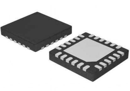


 工商网监
湘ICP备2023018690号
工商网监
湘ICP备2023018690号

