LTC3589/LTC3589-1/
LTC3589-2
8-Output Regulator with
Sequencing and I2C
Features
Description
Triple I2C Adjustable High Efficiency Step-Down DC/
DC Converters: 1.6A, 1A/1.2A, 1A/1.2A
nn High Efficiency 1.2A Buck-Boost DC/DC Converter
nn Triple 250mA LDO Regulators
nn Pushbutton ON/OFF Control with System Reset
nn Flexible Pin-Strap Sequencing Operation
nn I2C and Independent Enable Control Pins
nn Power Good and Reset Outputs
nn Dynamic Voltage Scaling and Slew Rate Control
nn Selectable 2.25MHz or 1.12MHz Switching Frequency
nn Always-Alive 25mA LDO Regulator
nn 8µA Standby Current
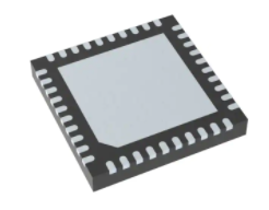
nn 40-Pin 6mm × 6mm × 0.75mm QFN
The LTC®3589 is a complete power management solution for ARM and ARM-based processors and advanced
portable microprocessor systems. The device contains
three step-down DC/DC converters for core, memory and
SoC rails, a buck-boost regulator for I/O at 1.8V to 5V and
three 250mA LDO regulators for low noise analog supplies. An I2C serial port is used to control enables, output
voltage levels, dynamic voltage scaling, operating modes
and status reporting. Differences between the LTC3589,
LTC3589-1, and LTC3589-2 are summarized in Table 1.
nn
Applications
Handheld Instruments and Scanners
Portable Industrial Devices
nn Automotive Infotainment
nn Medical Devices
nn High End Consumer Devices
nn Multirail Systems
nn Supports Freescale i.MX53/51, Marvell PXA and
Other Application Processors
Regulator start-up is sequenced by connecting outputs to
enable pins in the desired order or programmed via the
I2C port. System power-on, power-off, and reset functions
are controlled by pushbutton interface, pin inputs, or I2C
interface.
The LTC3589 supports i.MX53/51, PXA and OMAP processors with eight independent rails at appropriate power
levels. Other features include interface signals such as
the VSTB pin that simultaneously toggle up to four rails
between programmed run and standby output voltages.
The device is available in a low profile 40-pin 6mm × 6mm
exposed pad QFN package.
nn
nn
L, LT, LTC, LTM, Burst Mode, Linear Technology and the Linear logo are registered trademarks
of Linear Technology Corporation. All other trademarks are the property of their respective owners.
Typical Application
Start-Up Sequence
VIN 2.7V TO 5.5V
0.8V TO VIN
AT 25mA
LDO1_STBY
1µH
SW1
22µF
1µF
0.36V TO VIN
AT 250mA
1µF
1.5µH
SW2
LDO2
22µF
LTC3589
1.5µH
1.8V
AT 250mA
2.8V
AT 250mA
VIN
LDO3
1µF
3
7
BB_OUT
WAKE
(1V/DIV)
0.5V TO VIN
AT 1A
0.5V TO VIN
AT 1A
SW3
1µF
0.5V TO VIN
AT 1.6A
22µF
SW2
0.5V/DIV
LDO3
SW3
LDO2
2.7µH
LDO4
SW1
SW4AB
I2C
SW4CD
ENABLES
500µs/DIV
PWR_ON
WAKE
ON
GND
STATUS
3589 TA01b
1.8V TO 5V
BB_OUT
4
22µF
3589 TA01a
3589fh
For more information www.linear.com/LTC3589
1
�LTC3589/LTC3589-1/
LTC3589-2
Table of Contents
Features............................................................................................................................. 1
Applications........................................................................................................................ 1
Typical Application ................................................................................................................ 1
Description......................................................................................................................... 1
Absolute Maximum Ratings...................................................................................................... 3
Pin Configuration.................................................................................................................. 3
Order Information.................................................................................................................. 3
Electrical Characteristics......................................................................................................... 4
Typical Performance Characteristics........................................................................................... 9
Pin Functions......................................................................................................................13
Block Diagram.....................................................................................................................15
Operation..........................................................................................................................16
Introduction........................................................................................................................................................... 16
LTC3589, LTC3589-1, and LTC3589-2 Functional Comparison.............................................................................. 17
Always-On LDO...................................................................................................................................................... 17
Step-Down Switching Regulators.......................................................................................................................... 20
Buck-Boost Switching Regulator........................................................................................................................... 24
Slewing DAC Reference Operation......................................................................................................................... 28
Pushbutton Operation............................................................................................................................................ 29
Enable and Power-On Sequencing......................................................................................................................... 31
Fault Detection, Shutdown, and Reporting............................................................................................................. 32
I2C Operation......................................................................................................................................................... 36
Thermal Considerations and Board Layout............................................................................................................ 42
Typical Application...............................................................................................................46
Package Description.............................................................................................................48
Revision History..................................................................................................................49
Typical Application...............................................................................................................50
Related Parts......................................................................................................................50
2
3589fh
For more information www.linear.com/LTC3589
�LTC3589/LTC3589-1/
LTC3589-2
Absolute Maximum Ratings
(Notes 1, 3)
VIN, DVDD, SW1, SW2, SW3, SW4AB, SW4CD..... –0.3V to 6V
SW1, SW2, SW3, SW4AB, SW4CD
(Transients < 1µs, Duty Cycle < 5%)................ –2V to 7V
PVIN1, PVIN2, PVIN3, PVIN4................ –0.3V to VIN + 0.3V
VIN_LDO2, VIN_LDO34.......................... –0.3V to VIN + 0.3V
LDO1_STBY, LDO1_FB, BUCK1_FB, BUCK2_FB,
BUCK3_FB, BB_FB, BB_OUT, LDO2, LDO2_FB, LDO3,
LDO4, PGOOD, VSTB, EN1, EN2, EN3, EN4, EN_LDO2,
EN_LDO34, EN_LDO3, ON, PBSTAT, WAKE, RSTO,
PWR_ON, IRQ, ............................................ –0.3V to 6V
SDA, SCL.......................................–0.3V to DVDD + 0.3V
Operating Junction Temperature Range
(Note 2)................................................... –40°C to 150°C
Storage Temperature Range................... –65°C to 150°C
Pin Configuration
LTC3589-1/LTC3589-2
SDA
DVDD
BUCK2_FB
BUCK3_FB
LDO1_FB
LDO1_STBY
VIN
LDO2_FB
40 39 38 37 36 35 34 33 32 31
40 39 38 37 36 35 34 33 32 31
VIN_LDO2 1
TOP VIEW
BB_FB
SDA
DVDD
BUCK2_FB
BUCK3_FB
LDO1_FB
LDO1_STBY
VIN
LDO2_FB
BUCK1_FB
BB_FB
TOP VIEW
BUCK1_FB
LTC3589
30 SCL
VIN_LDO2 1
30 SCL
LDO2 2
29 PGOOD
LDO2 2
29 PGOOD
LDO3 3
28 VSTB
LDO3 3
28 VSTB
LDO4 4
27 PVIN3
LDO4 4
27 PVIN3
26 SW3
VIN_LDO34 5
25 SW2
PVIN1 6
SW1 7
24 PVIN2
SW1 7
24 PVIN2
RSTO 8
23 WAKE
RSTO 8
23 WAKE
VIN_LDO34 5
41
GND
PVIN1 6
EN_LDO2 9
22 PBSTAT
EN1 10
25 SW2
EN_LDO2 9
22 PBSTAT
EN1 10
PWR_ON
SW4CD
EN_LDO3
IRQ
BB_OUT
PVIN4
EN4
EN3
UJ PACKAGE
40-LEAD (6mm × 6mm) PLASTIC QFN
UJ PACKAGE
40-LEAD (6mm × 6mm) PLASTIC QFN
TJMAX = 150°C, θJA = 33°C/W
EXPOSED PAD (PIN 41) IS GND, MUST BE SOLDERED TO PCB
Order Information
SW4AB
PWR_ON
SW4CD
EN_LDO34
IRQ
BB_OUT
PVIN4
EN4
EN3
11 12 13 14 15 16 17 18 19 20
SW4AB
11 12 13 14 15 16 17 18 19 20
EN2
21 ON
EN2
21 ON
26 SW3
41
GND
TJMAX = 150°C, θJA = 33°C/W
EXPOSED PAD (PIN 41) IS GND, MUST BE SOLDERED TO PCB
http://www.linear.com/product/LTC3589#orderinfo
LEAD FREE FINISH
TAPE AND REEL
PART MARKING*
PACKAGE DESCRIPTION
TEMPERATURE RANGE
LTC3589EUJ#PBF
LTC3589EUJ#TRPBF
LTC3589UJ
40-Lead (6mm × 6mm) Plastic QFN
–40°C to 125°C
LTC3589IUJ#PBF
LTC3589IUJ#TRPBF
LTC3589UJ
40-Lead (6mm × 6mm) Plastic QFN
–40°C to 125°C
LTC3589HUJ#PBF
LTC3589HUJ#TRPBF
LTC3589UJ
40-Lead (6mm × 6mm) Plastic QFN
–40°C to 150°C
LTC3589EUJ-1#PBF
LTC3589EUJ-1#TRPBF
LTC3589UJ-1
40-Lead (6mm × 6mm) Plastic QFN
–40°C to 125°C
LTC3589IUJ-1#PBF
LTC3589IUJ-1#TRPBF
LTC3589UJ-1
40-Lead (6mm × 6mm) Plastic QFN
–40°C to 125°C
LTC3589HUJ-1#PBF
LTC3589HUJ-1#TRPBF
LTC3589UJ-1
40-Lead (6mm × 6mm) Plastic QFN
–40°C to 150°C
LTC3589EUJ-2#PBF
LTC3589EUJ-2#TRPBF
LTC3589UJ-2
40-Lead (6mm × 6mm) Plastic QFN
–40°C to 125°C
LTC3589IUJ-2#PBF
LTC3589IUJ-2#TRPBF
LTC3589UJ-2
40-Lead (6mm × 6mm) Plastic QFN
–40°C to 125°C
LTC3589HUJ-2#PBF
LTC3589HUJ-2#TRPBF
LTC3589UJ-2
40-Lead (6mm × 6mm) Plastic QFN
–40°C to 150°C
Consult LTC Marketing for parts specified with wider operating temperature ranges. *The temperature grade is identified by a label on the shipping container.
For more information on lead free part marking, go to: http://www.linear.com/leadfree/
For more information on tape and reel specifications, go to: http://www.linear.com/tapeandreel/. Some packages are available in 500 unit reels through
designated sales channels with #TRMPBF suffix.
3589fh
For more information www.linear.com/LTC3589
3
�LTC3589/LTC3589-1/
LTC3589-2
Electrical
Characteristics
The l denotes the specifications which apply over the specified operating
junction temperature range, otherwise specifications are at TA = 25°C (Note 2). VIN = PVIN1 = PVIN2 = PVIN3 = PVIN4 = VIN_LDO2 = VIN_LDO34
= DVDD = 3.8V. All regulators disabled unless otherwise noted.
SYMBOL
PARAMETER
VIN
Operating Input Supply Voltage, VIN
ISTANDBY
VIN Standby Current
fOSC
Oscillator Frequency
CONDITIONS
MIN
l
All Enables = 0V, PWR_ON = 0V, ILDO1 = 0mA
TYP
2.7
MAX
5.5
UNITS
V
8
18
µA
2.25
2.6
MHz
l
120
200
µA
l
23
40
µA
50
nA
l
l
1.8
Step-Down Switching Regulators 1, 2, and 3
Pulse-Skipping Mode VIN Quiescent Current
per Buck
Burst Mode® VIN Quiescent Current per Buck
VFB = 0.85V (Note 5)
IFB
Feedback Pin Input Current
VFB = 0.8V
–50
DX
Maximum Duty Cycle
VFB = 0V
100
RSW
SW Pull-Down Resistance
Regulators Disabled
2.5
kΩ
tSS
Soft-Start Rate
(Note 6)
0.8
V/ms
VFB(MAX)
Maximum Feedback Voltage
BxDTV1 = BxDTV2 = 11111,
VIN = 2.7V to 5.5V
l
0.735
0.75
VFB(LSB)
Feedback LSB Step Size
VFB(MIN)
Minimum Feedback Voltage
BxDTV1 = BxDTV2 = 00000,
VIN = 2.7V to 5.5V
l
0.351
0.3625
l
2.0
IVIN
%
0.765
12.5
V
mV
0.374
V
1.6A Step-Down Switching Regulator 1
ILIM1
Peak PMOS Current Limit SW1
2.7
A
RP1
RDS(ON) of PMOS1
ISW1 = –100mA
180
mΩ
RN1
RDS(ON) of NMOS1
ISW1 = 100mA
110
mΩ
1.0A/1.2A Step-Down Switching Regulators 2 and 3
ILIM2, 3
Peak PMOS Current Limit SW2 and SW3 (LTC3589)
Peak PMOS Current Limit SW2 and SW3 (LTC3589-1/
LTC3589-2)
l
1.5
1.9
A
l
1.8
2.3
A
RP2, 3
RDS(ON) of PMOS2 and PMOS3
ISW1 = –100mA
250
mΩ
RN2, 3
RDS(ON) of NMOS2 and NMOS3
ISW1 = 100mA
130
mΩ
1.2A Buck-Boost Switching Regulator 4 (Buck-Boost)
IVIN
PWM Mode VIN Quiescent Current
Burst Mode VIN Quiescent Current
VBB_FB = 0.85V (Note 5)
l
l
VBB_FB
Feedback Voltage
VIN = 2.7V to 5.5V
l
VOUTBB
Output Voltage Range
ILIM4
Peak PMOS Current Limit SW4AB
IPEAK4
Forward Burst Current Limit (Switch A)
ILIMR4
Reverse Current Limit (Switch D)
IZERO4
Reverse Burst Current Limit (Switch D)
Burst Mode Operation
0
mA
RP4
RDS(ON) of Switch A and Switch D
ISW4AB = ISW4CD = 100mA
160
mΩ
RN4
RDS(ON) of Switch B and Switch C
ISW4AB = ISW4CD = –100mA
110
mΩ
ROUT4
BB_OUT Pull-Down Resistance
Regulator Disabled
2.5
kΩ
tSS
Soft-Start Rate
(Note 6)
IFB
Feedback Pin Input Current
VFB = 0.85V
4
0.776
115
19
170
35
µA
µA
0.8
0.824
V
5.0
V
1.8
l
2.3
Burst Mode Operation
2.9
A
600
mA
1
A
2
–50
V/ms
50
nA
3589fh
For more information www.linear.com/LTC3589
�LTC3589/LTC3589-1/
LTC3589-2
Electrical Characteristics
The l denotes the specifications which apply over the specified operating
junction temperature range, otherwise specifications are at TA = 25°C (Note 2). VIN = PVIN1 = PVIN2 = PVIN3 = PVIN4 = VIN_LDO2 = VIN_LDO34
= DVDD = 3.8V. All regulators disabled unless otherwise noted.
SYMBOL
PARAMETER
CONDITIONS
MIN
TYP
MAX
UNITS
LDO Regulators
tLDO_SS
Soft-Start Time LDO2, LDO3, LDO4
100
µs
RLDO_PD
Output Pull-Down Resistance LDO2, LDO3, LDO4 LDO Disabled
2.5
kΩ
Always-On Regulator (LDO1_STBY)
VLDO1_FB
LDO1 Feedback Voltage
VLDO1
LDO1 Line Regulation
ILDO1_STBY = 1mA, LDO1_STBY = 1.2V,
VIN = 2.7V to 5.5V
0.15
%/V
LDO1 Load Regulation
ILDO1 = 0.1mA to 25mA,
LDO1_STBY = 1.2V
0.1
%
l
ILDO1
Available Output Current
ILDO1_SC
Short-Circuit Output Current Limit
VDROP1
Dropout Voltage (Note 4)
ILDO1 = 25mA, LDO1_STBY = 3.3V
ILDO1_FB
LDO1_FB Input Current
VLDO1_FB = 0.85V
l
0.76
0.8
0.84
25
V
mA
65
100
200
mA
mV
–50
50
nA
1.7
VIN
V
20
1
µA
µA
LDO Regulator 2 (LDO2)
VIN_LDO2
VIN_LDO2 Input Voltage Range
IVIN_LDO2
VIN_LDO2 Quiescent Current
VIN_LDO2 Shutdown Current
IVIN
VFB2(MAX)
VFB2(LSB)
LDO2 Feedback LSB Step Size
VFB2(MIN)
l
Regulator Enabled
Regulator Disabled
l
l
VIN Quiescent Current
EN_LDO2 = High
l
50
85
µA
LDO2 Maximum Feedback Voltage
L2DTV1 = L2DTV2 = 11111
l
0.735
0.75
0.765
V
LDO2 Minimum Feedback Voltage
L2DTV1 = L2DTV2 = 00000
VIN_LDO2 = VIN = 2.7V to 5.5V,
ILDO2 = 1mA
l
0.351
0.3625
LDO2 Line Regulation
ILDO2 =1mA, VIN_LDO2 = 2.7V to 5.5V
0.01
%/V
LDO2 Load Regulation
ILDO2 = 1mA to 250mA
0.01
%
12
0
12.5
ILDO2
LDO2 Available Output Current
ILDO2_SC
LDO2 Short-Circuit Current Limit
VDROP2
Dropout Voltage (Note 4)
ILDO2 = 200mA, VLDO2 = 2.5V
ILDO2 = 200mA, VLDO2 = 1.2V
ILDO2_FB
LDO2_FB Input Current
VLDO2_FB = 0.8V
l
mV
0.374
250
300
V
mA
450
600
mA
140
350
180
500
mV
mV
–50
50
nA
2.35
3.0
VIN
VIN
V
V
LDO Regulator 3 (LDO3)
VIN_LDO34
VIN_LDO34 Input Range (LTC3589)
VIN_LDO34 Input Range (LTC3589-1/LTC3589-2)
IVIN_LDO34
VIN_LDO34 Quiescent Current
VIN_LDO34 Shutdown Current
Regulator Enabled
Regulator Disabled
l
l
15
0
29
1
µA
µA
IVIN
VIN Quiescent Current
EN_LDO3 = High
l
50
85
µA
VLDO3
LDO3 Output Voltage (LTC3589)
LDO3 Output Voltage (LTC3589-1/LTC3589-2)
VIN_LDO34 = VIN = 2.7V to 5V,
ILDO3 = 1mA
l
l
1.8
2.8
1.854
2.884
V
V
LD03 Line Regulation
ILDO3 =1mA, VIN_LDO34 = 2.7V to 5.5V
0.01
%/V
LDO3 Load Regulation
ILDO3 = 1mA to 250mA
0.05
%
ILDO3
LDO3 Available Output Current
ILDO3_SC
LDO3 Short-Circuit Current Limit
VDROP3
LDO3 Dropout Voltage (LTC3589) (Note 4)
LDO3 Dropout Voltage (LTC3589-1/LTC3589-2)
(Note 4)
l
l
l
1.746
2.716
250
300
ILDO3 = 200mA, VLDO3 = 1.8V
ILDO3 = 200mA, VLDO3 = 2.8V
mA
450
600
mA
190
140
250
180
mV
mV
3589fh
For more information www.linear.com/LTC3589
5
�LTC3589/LTC3589-1/
LTC3589-2
Electrical Characteristics
The l denotes the specifications which apply over the specified operating
junction temperature range, otherwise specifications are at TA = 25°C (Note 2). VIN = PVIN1 = PVIN2 = PVIN3 = PVIN4 = VIN_LDO2 = VIN_LDO34
= DVDD = 3.8V. All regulators disabled unless otherwise noted.
SYMBOL
PARAMETER
CONDITIONS
MIN
TYP
MAX
UNITS
VIN
VIN
V
V
LDO Regulator 4 (LDO4)
VIN_LDO34
VIN_LDO34 Input Range (LTC3589)
VIN_LDO34 Input Range (LTC3589-1/LTC3589-2)
IVIN_LDO34
VIN_LDO34 Quiescent Current
VIN_LDO34 Shutdown Current
Regulator Enabled
Regulator Disabled
l
l
14
0
24
1
µA
µA
IVIN
VIN Quiescent Current
EN_LDO4 = High
l
50
85
µA
VLDO4
(LTC3589)
LDO 4 Output Voltage
ILDO4 = 1mA, L2DTV2[6:5] = 00
L2DTV2[6:5] = 01
L2DTV2[6:5] = 10
L2DTV2[6:5] = 11
l
l
l
l
2.716
2.425
1.746
3.201
2.8
2.5
1.8
3.3
2.884
2.575
1.854
3.399
V
V
V
V
LDO 4 Output Voltage
VLDO4
(LTC3589-1)
(LTC3589-2)
ILDO4 = 1mA, L2DTV2[6:5] = 00
L2DTV2[6:5] = 01
L2DTV2[6:5] = 10
L2DTV2[6:5] = 11
l
l
l
l
1.164
1.746
2.425
3.104
1.2
1.8
2.5
3.2
1.236
1.854
2.575
3.296
V
V
V
V
l
l
2.35
1.7
LD04 Line Regulation
ILDO4 =1mA, VIN_LDO34 = 2.7V to 5.5V,
VOUT = 1.8V
0.01
%/V
LDO4 Load Regulation
ILDO4 = 1mA to 250mA
0.05
%
ILDO4
LDO4 Available Output Current
ILDO4_SC
LDO4 Short-Circuit Current Limit
VDROP4
LDO4 Dropout Voltage (Note 4)
ILDO4 = 200mA, VLDO4 = 3.3V
ILDO4 = 200mA, VLDO4 = 1.8V
ILDO4 = 200mA, VLDO4 = 3.2V (LTC3589-1/
LTC3589-2)
VENx_THR
Threshold Rising
All Enables Low
l
VENx_THR2
VENx_THF2
Threshold Rising
Threshold Falling
Any Enable High
Any Enable High
l
l
RENX
Input Pull-Down Resistance
l
250
300
mA
450
600
mA
120
190
120
160
250
160
mV
mV
mV
0.8
1.2
V
0.5
0.45
0.530
V
V
Enable Inputs
0.420
4.5
MΩ
VSTB, PWR_ON Inputs
VVSTB_THR
VVSTB_THF
VSTB Pin Threshold Rising
VSTB Pin Threshold Falling
RVSTB
Pull-Down Resistance
l
l
0.8
0.7
1.2
4.5
VPWR_ONTHR PWR_ON Pin Threshold Rising
VPWR_ONTHF PWR_ON Pin Threshold Falling
RPWR_ON
0.4
l
l
0.4
Pull-Down Resistance
0.8
0.7
V
V
MΩ
1.2
4.5
V
V
MΩ
I2C Port
DVDD
DVDD Input Supply Voltage
IDVDD
DVDD Quiescent Current
VDVDD_UVLO
DVDD UVLO Level
ADDRESS
Device Address – Write
Device Address – Read
l
5.5
V
0.5
µA
0.8
V
01101000
01101001
VIH SDA, SCL SDA and SCL Input Threshold Rising
VIL SDA, SCL SDA and SCL Input Threshold Falling
70
IIHSCx IILSCx
SDA and SCL Input Current
SDA = SCL = 0V to 5.5V
VOL SDA
SDA Output Low Voltage
ISDA = 3mA
fSCL
SCL Clock Operating Frequency
6
1.6
SCL/SDA = 0kHz
–250
l
30
%DVDD
%DVDD
250
nA
0.4
V
400
kHz
3589fh
For more information www.linear.com/LTC3589
�LTC3589/LTC3589-1/
LTC3589-2
Electrical Characteristics
The l denotes the specifications which apply over the specified operating
junction temperature range, otherwise specifications are at TA = 25°C (Note 2). VIN = PVIN1 = PVIN2 = PVIN3 = PVIN4 = VIN_LDO2 = VIN_LDO34
= DVDD = 3.8V. All regulators disabled unless otherwise noted.
SYMBOL
PARAMETER
CONDITIONS
MIN
TYP
MAX
UNITS
tSU_STA
Repeated Start Condition Set-Up Time
0.6
µs
tSU_STO
Stop Condition Set-Up Time
0.6
µs
tHD_DAT(O)
Data Hold Time Output
0
tHD_DAT(I)
Data Hold Time Input
0
ns
tSU_DAT
Data Set-Up Time
100
ns
tLOW
SCL Clock Low Period
1.3
µs
tHIGH
SCL Clock High Period
0.6
µs
tf
Data Fall Time
CB = Capacitance of One BUS Line (pF)
20 + 0.1CB
300
ns
tr
Data Rise Time
CB = Capacitance of One BUS Line (pF)
20 + 0.1CB
300
ns
tSP
Input Spike Suppression Pulse Width
50
ns
1.2
V
V
100
nA
µA
900
ns
Pushbutton Interface
VON_THR
VON_THF
ON Threshold Rising
ON Threshold Falling
ION
ON Input Current
tON_PBSTAT1
ON Low Time to PBSTAT Low
tON_PBSTAT2
ON High Time to PBSTAT High
0.2
µs
tON_WAKE
ON Low Time to WAKE High
400
ms
tON_HR
ON Low Time to Hard Reset
5
s
tPBSTAT_PW
PBSTAT Minimum Pulse Width
50
ms
tPBSTAT_BK
PBSTAT Blanking from WAKE Low
1
s
tWAKE_OFF
Minimum WAKE Low Time
1
s
tWAKE_ON
WAKE High Time with PWR_ON = 0V
5
s
tPWR_ON
PWR_ON to WAKE High (LTC3589)
PWR_ON to WAKE High (LTC3589-1/LTC3589-2)
50
2
ms
ms
tPWR_OFF
PWR_ON to WAKE Low (LTC3589)
PWR_ON to WAKE Low (LTC3589-1/LTC3589-2)
50
2
ms
ms
l
l
ON = VIN
ON = 0V
0.4
–100
0.8
0.7
40
50
ms
Status Output Pins (PBSTAT, WAKE, PGOOD, RSTO, IRQ)
VPBSTAT
PBSTAT Output Low Voltage
IPBSTAT = 3mA
IPBSTAT
PBSTAT Output High Leakage Current
VPBSTAT = 3.8V
VWAKE
WAKE Output Low Voltage
IWAKE = 3mA
IWAKE
WAKE Output High Leakage Current
VWAKE = 3.8V
VPGOOD
PGOOD Output Low Voltage
IPGOOD = 3mA
VPGOOD = 3.8V
0.1
–0.1
0.1
–0.1
0.1
–0.1
0.4
V
0.1
µA
0.4
V
0.1
µA
0.4
V
0.1
µA
IPGOOD
PGOOD Output High Leakage Current
VPGOOD
PGOOD Threshold Rising
PGOOD Threshold Falling
–6
–8
%
%
VNRSTO
LDO1 Power Good Threshold Rising
LDO1 Power Good Threshold Falling
–6
–8
%
%
VUVLO
Undervoltage Lockout Rising
Undervoltage Lockout Falling
2.65
2.55
2.7
V
V
3589fh
For more information www.linear.com/LTC3589
7
�LTC3589/LTC3589-1/
LTC3589-2
Electrical
Characteristics
The l denotes the specifications which apply over the specified operating
junction temperature range, otherwise specifications are at TA = 25°C (Note 2). VIN = PVIN1 = PVIN2 = PVIN3 = PVIN4 = VIN_LDO2 = VIN_LDO34
= DVDD = 3.8V. All regulators disabled unless otherwise noted.
SYMBOL
PARAMETER
CONDITIONS
VUVWARN
Undervoltage Warning Rising
Undervoltage Warning Falling
VRSTO
RSTO Output Low Voltage
IRSTO = 3mA
IRSTO
RSTO Output High Leakage Current
VRSTO = 3.8V
VIRQ
IRQ Output Low Voltage
IIRQ = 3mA
IIRQ
IRQ Output High Leakage Current
VIRQ = 3.8V
TYP
MAX
UNITS
3
2.9
Note 1: Stresses beyond those listed Under Absolute Maximum ratings
may cause permanent damage to the device. Exposure to any Absolute
Maximum rating condition for extended periods may affect device
reliability and lifetime.
Note 2: The LTC3589 are tested under pulsed load conditions such
that TJ ≈ TA. The LTC3589E are guaranteed to meet specifications from
0°C to 85°C junction temperature. Specifications over the –40°C to
125°C operating junction temperature range are assured by design,
characterization and correlation with statistical process controls. The
LTC3589I are guaranteed over the –40°C to 125°C operating junction
temperature range and the LTC3589H are guaranteed over the full
–40°C to 150°C operating junction temperature range. High junction
temperatures degrade operating lifetimes; operating lifetime is derated for
junction temperatures greater than 125°C. The junction temperature (TJ
in °C) is calculated from the ambient temperature (TA in °C) and power
dissipation (PD, in Watts) according to the formula:
TJ = TA + (PD • θJA), where the package junction to ambient thermal
impedance θJA = 33°C/W.
8
MIN
0.1
–0.1
0.1
–0.1
0.4
V
0.1
µA
0.4
V
0.1
µA
Note that the maximum ambient temperature consistent with these
specifications is determined by specific operating conditions in
conjunction with board layout, the rated package thermal impedance and
other environmental factors.
Note 3: The LTC3589 include overtemperature protection that is intended
to protect the device during momentary overload conditions. Junction
temperature will exceed 150°C when overtemperature protection is active.
Continuous operation above the specified maximum operating temperature
may impair device reliability.
Note 4: Dropout voltage is defined as (VIN – VLDO) for LDO1 or
(VIN_LDO – VLDO) for other LDOs when VLDO is 3% lower than VLDO
measured with VIN = VIN_LDO = 4.3V.
Note 5: Dynamic supply current is higher due to the gate charge being
delivered at the switching frequency.
Note 6: Soft-start measured in test mode with regulator error amplifier in
unity gain mode.
3589fh
For more information www.linear.com/LTC3589
�LTC3589/LTC3589-1/
LTC3589-2
Typical Performance Characteristics
14
Standby IVIN vs VIN
250
12
VIN = 3.8V, TA = 25°C, unless otherwise noted.
LDO2 to LDO4 IVIN vs VIN
900
600
IVIN (µA)
ENABLE TWO LDOs
150
IVIN (µA)
IVIN (µA)
6
ENABLE ONE LDO
100
3.0
3.5
4.0
VIN (V)
4.5
5.0
0
2.5
5.5
3.0
3.5
4.0
VIN (V)
4.5
5.0
1200
400
20
200
3.0
3.5
4.0
VIN (V)
4.5
5.0
ALL REGULATORS ENABLED
Burst Mode OPERATION
STANDBY (ONLY LDO1 ON)
0
1.0
25 50 75 100 125
TEMPERATURE (°C)
PERCENT CHANGE (%)
2.25
2.05
2.00
1.95
–50
30
110
70
TEMPERATURE (°C)
150
3589 G07
3.0
3.5
4.0
VIN (V)
5.0
4.5
100
0.8
90
0.6
80
0.4
0.2
0
–0.2
–0.4
–0.8
2.5
Buck-Boost Efficiency vs IOUT
VIN = 3.8V
60
50
PWM MODE
40
30
VOUT = 5.0V
VOUT = 2.5V
VOUT = 3.3V
10
3.5
4.5
4.0
VIN (V)
5.0
5.5
3589 G08
BURST
70
20
3.0
5.5
3589 G06
Switching Frequency Change vs VIN
–0.6
–10
0
2.5
150
EFFICIENCY (%)
2.30
2.10
Burst Mode OPERATION
50
3589 G05
Oscillator Frequency
vs Temperature
2.15
200
150
3589 G04
2.20
250
100
0
–50 –25
5.5
5.5
PWM MODE
300
600
40
0
2.5
5.0
4.5
4.0
VIN (V)
Buck-Boost IVIN vs VIN
350
IVIN (µA)
ENABLE ONE BUCK
3.5
400
ALL REGULATORS ENABLED
PULSE-SKIPPING MODE
800
IVIN (µA)
60
450
1000
ENABLE THREE BUCKS
ENABLE TWO BUCKS
3.0
3589 G03
Input Supply Current
vs Temperature
Burst Mode OPERATION
80
0
2.5
5.5
3589 G02
Step-Down Switching Regulator
IVIN vs VIN
100
IVIN (µA)
ENABLE ONE BUCK
100
3589 G01
FREQUENCY (MHz)
400
200
50
0
2.5
120
ENABLE TWO BUCKS
500
300
4
2
ENABLE THREE BUCKS
700
10
8
PULSE-SKIPPING MODE
800
ENABLE THREE LDOs
200
Step-Down Switching Regulator
IVIN vs VIN
0
0.01
0.1
1
10
100
LOAD CURRENT (mA)
1000
3589 G9
3589fh
For more information www.linear.com/LTC3589
9
�LTC3589/LTC3589-1/
LTC3589-2
Typical Performance Characteristics
90
BURST
80
70
60
PWM MODE
50
40
30
20
10
0
0.01
0.1
1
10
100
LOAD CURRENT (mA)
90
60
50
FORCED
CONTINUOUS
40
30
20
10
1000
0.1
1
10
100
LOAD CURRENT (mA)
50
FORCED
CONTINUOUS
40
30
PULSE-SKIPPING
0
0.01
0.1
1
10
100
LOAD CURRENT (mA)
1000
3589 G12
Buck-Boost RDS(ON)
vs Temperature
0.40
0.25
0.35
BURST
70
PULSESKIPPING
60
50
0.20
0.30
FORCED
CONTINUOUS
40
RDS(ON) (Ω)
EFFICIENCY (%)
60
Step-Down Switching Regulator
RDS(ON) vs Temperature
VOUT = 3.3V
80
30
PMOS
BUCK2, 3 PMOS
0.25
BUCK1 PMOS
0.20
BUCK2, 3 NMOS
0.15
0.10
20
BUCK1 NMOS
0.15
NMOS
0.10
0.05
0.05
10
0
0.01
0.1
1
10
100
LOAD CURRENT (mA)
0
–50
1000
–10
30
110
70
TEMPERATURE (°C)
3589 G13
CURRENT LIMIT (A)
BUCK2, BUCK3
(LTC3589-1/LTC3589-2)
2.0
BUCK2, BUCK3
1.5
1.0
110
30
70
TEMPERATURE (°C)
150
3589 G15
Step-Down Switching Regulator
Soft-Start
3.0
PEAK LIMIT
2.5
CLAMP LIMIT
VOUT
500mV/DIV
2.0
0
75 100 125 150
TEMPERATURE (°C)
25
50
3589 G16
IL
200mA/DIV
1.5
1.0
200µs/DIV
0.5
0.5
10
–10
3.5
BUCK1
3.0
0
–50 –25
0
–50
Buck-Boost Current Limit
vs Temperature
3.5
2.5
150
3589 G14
Step-Down Switching
Regulator Current Limit
vs Temperature
CURRENT LIMIT (A)
70
3589 G11
Step-Down Switching Regulator 3
Efficiency vs IOUT
90
BURST
10
1000
3589 G10
100
VOUT = 1.8V
20
PULSE-SKIPPING
0
0.01
Step-Down Switching Regulator 2
Efficiency vs IOUT
80
BURST
70
VIN = 5.0V
VIN = 4.2V
VIN = 3.0V
100
VOUT = 1.2V
80
EFFICIENCY (%)
EFFICIENCY (%)
100
VOUT = 3.3V
EFFICIENCY (%)
90
Step-Down Switching Regulator 1
Efficiency vs IOUT
RDS(ON) (Ω)
100
Buck-Boost Efficiency vs IOUT
VIN = 3.8V, TA = 25°C, unless otherwise noted.
0
–50 –25
0
3589 G18
25 50 75 100 125 150
TEMPERATURE (°C)
3589 G17
3589fh
For more information www.linear.com/LTC3589
�LTC3589/LTC3589-1/
LTC3589-2
Typical Performance Characteristics
Buck-Boost Switching Regulator
Soft-Start
VIN = 3.8V, TA = 25°C, unless otherwise noted.
Step-Down Switching Regulator 1
Load Step
Dynamic Voltage Slew
PULSE-SKIPPING MODE
1V/DIV
VOUT
VOUT
1V/DIV
VOUT
50mV/DIV
PGOOD
5V/DIV
500mA/DIV
100µs/DIV
ILOAD
VSTB
IL
5V/DIV
1A/DIV
200µs/DIV
3589 G19
Step-Down Switching Regulator 1
Load Step
40µs/DIV
3589 G20
VRRCR = 1.75mV/µs
LOAD CAPACITANCE = 44µF
Buck-Boost Switching Regulator 1
Load Step
Maximum Buck-Boost Load
Current vs VIN
2.5
Burst Mode OPERATION
VOUT
200mV/DIV
ILOAD
2.0
LOAD CURRENT (A)
VOUT
50mV/DIV
ILOAD
1A/DIV
1A/DIV
40µs/DIV
40µs/DIV
LOAD CAPACITANCE = 22µF
3589 G22
LOAD CAPACITANCE = 44µF
3589 G21
1.5
1.0
0.5
3589 G23
0
2.5
VOUT = 1.8V
VOUT = 3.3V
VOUT = 5V
3.0
3.5
4.0
VIN (V)
4.5
5.0
5.5
3589 G24
LDO1 Dropout Voltage
vs Temperature
LDO1 Short-Circuit Current
vs Temperature
LDO1 Output Change vs VIN
0.5
80
VLDO1 = 25mA
0.0
CHANGE IN VLDO1 (%)
DROPOUT VOLTAGE (mV)
VLDO1 = 1.8V
400
300
VLDO1 = 3.3V
200
–1.0
VLDO1 = 1.2V
VLDO1 = 1.8V
VLDO1 = 2.8V
VLDO1 = 3.3V
–1.5
100
0
–50 –25
–0.5
0
75 100 125 150
TEMPERATURE (°C)
25
50
3589 G25
–2.0
2
3
4
5
VIN (V)
3589 G26
SHORT-CIRCUIT CURRENT (mA)
500
70
60
50
40
30
20
–50 –25
0
25 50 75 100 125 150
TEMPERATURE (°C)
3589 G27
3589fh
For more information www.linear.com/LTC3589
11
�LTC3589/LTC3589-1/
LTC3589-2
Typical Performance Characteristics
LDO2, LDO3, LDO4 Dropout
Voltage vs Temperature
LDO2, LDO3, LDO4 Dropout
Voltage vs Load Current
LDO2, LDO3, LDO4 Short-Circuit
Current vs Temperature
500
DROPOUT VOLTAGE (mV)
VLDO = 1.2V
400
300
VLDO = 1.8V
200
VLDO = 3.3V
100
500
400
SHORT-CIRCUIT CURRENT (mA)
500
DROPOUT VOLTAGE (mV)
VIN = 3.8V, TA = 25°C, unless otherwise noted.
VLDO = 1.2V
300
VLDO = 1.8V
200
100
VLDO = 3.3V
0
–50 –25
0
25
50
75 100 125 150
TEMPERATURE (°C)
ILOAD = 200mA
3589 G28
0
0
1V/DIV
100
150
200
LOAD CURRENT (mA)
250
400
350
300
250
200
–50 –25
VLDO
50mV/DIV
LDO1 Load Step Response
1.8V
VLDO1
50mV/DIV
1.2V
VLDO2 =1.2V
220mA
20mA
ILDO
100mA/DIV
VEN_LDO2,VEN_LDO34
ILDO1
10mA/DIV
10mA
100µs/DIV
3589 G31
10µs/DIV
1mA
3589 G32
LOAD CAPACITANCE = 1µF
12
25 50 75 100 125 150
TEMPERATURE (°C)
3589 G30
LDO2, LDO3, LDO4 Load Step
Response
VLDO3 =1.8V
0
3589 G29
LDO2, LDO3, LDO4 Enable
Response
VLDO4 =2.8V
50
450
40µs/DIV
3589 G33
LOAD CAPACITANCE = 1µF
3589fh
For more information www.linear.com/LTC3589
�LTC3589/LTC3589-1/
LTC3589-2
Pin Functions
VIN_LDO2 (Pin 1): Power Input for LDO2. This pin should
be bypassed to ground with a 1µF or greater ceramic
capacitor.
LDO2 (Pin 2): Output Voltage of LDO2. Nominal output
voltage is set with a resistor feedback divider that servos to
an I2C register controlled DAC reference. This pin must be
bypassed to ground with a 1µF or greater ceramic capacitor.
LDO3 (Pin 3): Output Voltage of LDO3. Nominal output
voltage is fixed at 1.8V or 2.8V (LTC3589-1/LTC3589-2).
This pin must be bypassed to ground with a 1µF or greater
ceramic capacitor.
LDO4 (Pin 4): Output Voltage of LDO4. Output voltage is
selected via the I2C port. This pin must be bypassed to
ground with a 1µF or greater ceramic capacitor.
VIN_LDO34 (Pin 5): Power Input for LDO3 and LDO4. This
pin should be bypassed to ground with a 1µF or greater
ceramic capacitor.
PVIN1 (Pin 6): Power Input for Step-Down Switching
Regulator 1. Tie this pin to VIN supply. This pin should
be bypassed to ground with a 4.7µF or greater ceramic
capacitor.
SW1 (Pin 7): Switch Pin for Step-Down Switching
Regulator 1. Connect one side of step-down switching
regulator 1 inductor to this pin.
RSTO (Pin 8): Reset Output. Open-drain output pulls low
when the always-on regulator LDO1 is below regulation
and during a hard reset initiated by a pushbutton input.
EN_LDO2 (Pin 9): Enable LDO2 Logic Input. Active high
input to enable LDO2. A weak pull-down forces EN_LDO2
low when left floating.
EN1 (Pin 10): Enable Step-Down Switching Regulator 1.
Active high input to enable step-down switching
regulator 1. A weak pull-down forces EN1 low when left
floating.
EN2 (Pin 11): Enable Step-Down Switching Regulator 2.
Active high input to enable step-down switching
regulator 2. A weak pull-down forces EN2 low when left
floating.
SW4AB (Pin 12): Switch Pin for Buck-Boost Switching
Regulator 4. Connected to the buck-boost internal power
switches A and B. Connect an inductor between this pin
and SW4CD (Pin 19).
EN3 (Pin 13): Enable Step-Down Switching Regulator 3.
Active high input to enable step-down switching
regulator 3. A weak pull-down forces EN3 low when left
floating.
EN4 (Pin 14): Enable Buck-Boost Switching Regulator 4.
Active high input to enable buck-boost switching
regulator 4. A weak pull-down forces EN4 low when left
floating.
PVIN4 (Pin 15): Power Input for Switching Regulator 4.
Tie this pin to VIN supply. This pin should be bypassed to
ground with a 4.7µF or greater ceramic capacitor.
BB_OUT (Pin 16): Output Voltage of Buck-Boost Switching
Regulator 4. This pin must be bypassed to ground with a
22µF or greater ceramic capacitor.
IRQ (Pin 17): Interrupt Request Output. Open-drain
driver is pulled low for power good, undervoltage, and
overtemperature warning and fault conditions. Clear IRQ
by writing to the I2C CLIRQ command register.
EN_LDO34 (Pin 18): LTC3589 Enable LDO3 and LDO4
Logic Input. Active high to enable LDO3 and LDO4. Disable
LDO4 via I2C software commands using I2C command
registers OVEN or L2DTV2. A weak pull-down forces
EN_LDO34 low when left floating.
EN_LDO3 (Pin 18): LTC3589-1/LTC3589-2 Enable LDO3
Logic Input. Active high to enable LDO3. A weak pull-down
forces EN_LDO3 low when left floating.
SW4CD (Pin 19): Switch Pin for Buck-Boost Switching
Regulator 4. Connected to the buck-boost internal power
switches C and D. Connect an inductor between this node
and SW4AB (Pin 12).
PWR_ON (Pin 20): External Power-On. Handshaking pin
to acknowledge successful power-on sequence. PWR_ON
must be driven high within five seconds of WAKE going
high to keep power on. It can be used to activate the WAKE
output by driving high. Drive low to shut down WAKE.
3589fh
For more information www.linear.com/LTC3589
13
�LTC3589/LTC3589-1/
LTC3589-2
PIN FUNCTIONS
ON (Pin 21): Pushbutton Input. A weak internal pullup forces ON high when left floating. A normally open
pushbutton is connected from ON to ground to force a
low state on this pin.
PBSTAT (Pin 22): Pushbutton Status. Open-drain output
to be used for processor interrupts. PBSTAT mirrors the
status of ON pushbutton pin. PBSTAT is delayed 50ms
from ON pin for debounce.
WAKE (Pin 23): System Wake Up. Open-drain driver output
releases high when signaled by pushbutton activation or
PWR_ON input. It may be used to initiate a pin-strapped
power-up sequence by connecting to a regulator enable pin.
PVIN2 (Pin 24): Power Input for Step-Down Switching
Regulator 2. Tie this pin to VIN supply. This pin should
be bypassed to ground with a 4.7µF or greater ceramic
capacitor.
SW2 (Pin 25): Switch Pin for Step-Down Switching
Regulator 2. Connect one side of step-down switching
regulator 2 inductor to this pin.
SW3 (Pin 26): Switch Pin for Step-Down Switching
Regulator 3. Connect one side of step-down switching
regulator 3 inductor to this pin.
DVDD (Pin 32): Supply Voltage for I2C Serial Port. This
pin sets the logic reference level of SCL and SDA I2C pins.
DVDD resets I2C registers to power on state when driven to


 工商网监
湘ICP备2023018690号
工商网监
湘ICP备2023018690号

