LTC5542
1.6GHz to 2.7GHz
High Dynamic Range
Downconverting Mixer
DESCRIPTION
FEATURES
n
n
n
n
n
n
n
n
n
n
n
n
Conversion Gain: 8dB at 2.4GHz
IIP3: 26.8dBm at 2.4GHz
Noise Figure: 9.9dB at 2.4GHz
17.3dB NF Under +5dBm Blocking
High Input P1dB
3.3V Supply, 660mW Power Consumption
Shutdown Pin
50Ω Single-Ended RF and LO Inputs
LO Inputs 50Ω Matched when Shutdown
High Isolation LO Switch
0dBm LO Drive Level
High LO-RF and LO-IF Isolation
Small Solution Size
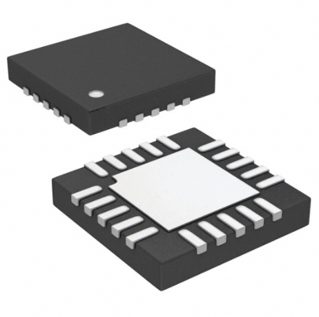
20-Lead (5mm × 5mm) QFN package
The LTC®5542 is part of a family of high dynamic range, high
gain, passive downconverting mixers covering the 600MHz
to 4GHz frequency range. The LTC5542 is optimized for
1.6GHz to 2.7GHz RF applications. The LO frequency
must fall within the 1.7GHz to 2.5GHz range for optimum
performance. A typical application is a LTE or WiMAX receiver
with a 2.3GHz to 2.7GHz RF input and low-side LO.
The LTC5542 is designed for 3.3V operation, however; the
IF amplifier can be powered by 5V for the highest P1dB.
An integrated SPDT LO switch with fast switching accepts
two active LO signals, while providing high isolation.
APPLICATIONS
The LTC5542’s high conversion gain and high dynamic
range enable the use of lossy IF filters in high-selectivity
receiver designs, while minimizing the total solution cost,
board space and system-level variation.
n
High Dynamic Range Downconverting Mixer Family
n
n
n
n
Wireless Infrastructure Receivers
(LTE, W-CDMA. TD-SCDMA, WiMAX, GSM1800)
Point-to-Point Microwave Links
High Dynamic Range Downmixer Applications
L, LT, LTC, LTM, Linear Technology and the Linear logo are registered trademarks of Linear
Technology Corporation. All other trademarks are the property of their respective owners.
PART#
RF RANGE
LO RANGE
LTC5540
600MHz –1.3GHz
700MHz – 1.2GHz
LTC5541
1.3GHz – 2.3GHz
1.4GHz – 2.0GHz
LTC5542
1.6GHz – 2.7GHz
1.7GHz – 2.5GHz
LTC5543
2.3GHz – 4GHz
2.4GHz – 3.6GHz
TYPICAL APPLICATION
Wideband Receiver
190MHz
SAW
1nF
VCCIF
3.3V or 5V
1μF
22pF
150nH
11.0
ADC
IF –
RF
2300MHz
TO
2400MHz
LO2
LTC5542
IF
RF
LNA
ALTERNATE LO FOR
FREQUENCY-HOPPING
LO
0.7pF
SYNTH 2
BIAS
SHDN
VCC2
VCC 3.3V
1μF
VCC1
22pF
VCC3
LO1
LOSEL
LO SELECT
(0V/3.3V)
IIP3 26
24
22
9.0
20
8.5
18
8.0 GC
7.5
16
±30MHz
14
7.0
4.7pF
SHDN
(0V/3.3V)
GC (dB)
4.7pF
IMAGE
BPF 22pF
28
10.5 RF = 2350 ±50MHz
LO = 2160MHz
10.0 P = 0dBm
LO
9.5 TEST CIRCUIT IN FIGURE 1
SYNTH 1
LO
2160MHz
IIP3 (dBm), SSB NF (dB)
IF+
190MHz
BPF
IF
AMP
1nF
150nH
Wideband Conversion Gain, IIP3
and NF vs IF Output Frequency
12
6.5
10
NF
6.0
8
140 150 160 170 180 190 200 210 220 230 240
IF OUTPUT FREQUENCY (MHz)
5542 TA01a
5542 TA01
5542f
1
�LTC5542
ABSOLUTE MAXIMUM RATINGS
PIN CONFIGURATION
(Note 1)
IFGND
GND
IF–
IFBIAS
IF+
TOP VIEW
Mixer Supply Voltage (VCC1, VCC2)...........................3.8V
LO Switch Supply Voltage (VCC3).............................3.8V
IF Supply Voltage (IF+, IF –) ......................................5.5V
Shutdown Voltage (SHDN) ................–0.3V to VCC +0.3V
LO Select Voltage (LOSEL)................–0.3V to VCC +0.3V
LO1, LO2 Input Power (1GHz to 3GHz) ...................9dBm
LO1, LO2 Input DC Voltage ....................................±0.5V
RF Input Power (1GHz to 3GHz) ...........................15dBm
RF Input DC Voltage ............................................... ±0.1V
Operating Temperature Range .................–40°C to 85°C
Storage Temperature Range .................. –65°C to 150°C
Junction Temperature (TJ) .................................... 150°C
20 19 18 17 16
15 LO2
NC 1
14 VCC3
RF 2
21
GND
CT 3
13 GND
7
8
9 10
LOSEL
GND
6
VCC1
11 LO1
VCC2
12 GND
SHDN 5
LOBIAS
GND 4
UH PACKAGE
20-LEAD (5mm s 5mm) PLASTIC QFN
TJMAX = 150°C, θJA = 34°C/W, θJC = 3°C/W
EXPOSED PAD (PIN 21) IS GND, MUST BE SOLDERED TO PCB
ORDER INFORMATION
LEAD FREE FINISH
TAPE AND REEL
PART MARKING
PACKAGE DESCRIPTION
TEMPERATURE RANGE
LTC5542IUH#PBF
LTC5542IUH#TRPBF
5542
20-Lead (5mm x 5mm) Plastic QFN
–40°C to 85°C
Consult LTC Marketing for parts specified with wider operating temperature ranges.
Consult LTC Marketing for information on non-standard lead based finish parts.
For more information on lead free part marking, go to: http://www.linear.com/leadfree/
For more information on tape and reel specifications, go to: http://www.linear.com/tapeandreel/
AC ELECTRICAL CHARACTERISTICS
VCC = 3.3V, VCCIF = 3.3V, SHDN = Low, TA = 25°C, PLO = 0dBm,
unless otherwise noted. Test circuit shown in Figure 1. (Notes 2, 3, 4)
PARAMETER
CONDITIONS
MIN
LO Input Frequency Range
RF Input Frequency Range
Low-Side LO
High-Side LO
TYP
MAX
UNITS
1700 to 2500
MHz
1900 to 2700
1600 to 2300
MHz
MHz
5 to 500
MHz
IF Output Frequency Range
Requires External Matching
RF Input Return Loss
ZO = 50Ω, 1600MHz to 2700MHz
>12
dB
LO Input Return Loss
ZO = 50Ω, 1700MHz to 2500MHz
>12
dB
IF Output Return Loss
Requires External Matching
>12
dB
LO Input Power
fLO = 1700MHz to 2500MHz
LO to RF Leakage
fLO = 1700MHz to 2500MHz
35
–4
0
6
dBm
dB
5542f
2
�LTC5542
AC ELECTRICAL CHARACTERISTICS
VCC = 3.3V, VCCIF = 3.3V, SHDN = Low, TA = 25°C, PLO = 0dBm,
PRF = –3dBm (Δf = 2MHz for two-tone IIP3 tests),unless otherwise noted. Test circuit shown in Figure 1. (Notes 2, 3, 4)
Low-Side LO Downmixer Application: RF = 1900 to 2700MHz, IF = 190MHz, fLO = fRF –fIF
PARAMETER
CONDITIONS
Conversion Gain
RF = 2150MHz
RF = 2400MHz
RF = 2650MHz
MIN
TYP
6.5
8.5
8.0
7.4
MAX
UNITS
dB
Conversion Gain Flatness
RF = 2350 ±30MHz, LO = 2160MHz, IF=190 ±30MHz
±0.15
dB
Conversion Gain vs Temperature
TA = –40ºC to +85ºC, RF = 2400MHz
–0.006
dB/°C
Input 3rd Order Intercept
RF = 2150MHz
RF = 2400MHz
RF = 2650MHz
27.2
26.8
25.3
dBm
RF = 2150MHz
RF = 2400MHz
RF = 2650MHz
9.9
9.9
10.2
dB
SSB Noise Figure Under Blocking
fRF = 2400MHz, fLO = 2210MHz,
fBLOCK = 2500MHz, PBLOCK = 5dBm
17.3
dB
2RF – 2LO Output Spurious Product
(fRF = fLO + fIF/2)
fRF = 2305MHz at –10dBm, fLO = 2210MHz, fIF = 190MHz
–62
dBc
3RF – 3LO Output Spurious Product
(fRF = fLO + fIF/3)
fRF = 2273.33MHz at –10dBm, fLO = 2210MHz, fIF = 190MHz
–73
dBc
Input 1dB Compression
RF = 2400MHz, VCCIF = 3.3V
RF = 2400MHz, VCCIF = 5V
11.3
14.7
dBm
SSB Noise Figure
24.0
High-Side LO Downmixer Application: RF = 1600-2300MHz, IF = 190MHz, fLO = fRF +fIF
PARAMETER
CONDITIONS
Conversion Gain
RF = 1750MHz
RF = 1950MHz
RF = 2150MHz
MIN
TYP
6.5
8.8
8.5
8.0
MAX
UNITS
dB
Conversion Gain Flatness
RF = 1950MHz ±30MHz, LO = 2140MHz, IF = 190 ±30MHz
±0.20
dB
Conversion Gain vs Temperature
TA = –40°C to 85°C, RF = 1950MHz
–0.006
dB/°C
Input 3rd Order Intercept
RF = 1750MHz
RF = 1950MHz
RF = 2150MHz
25.1
25.2
24.6
dBm
SSB Noise Figure
23.0
RF = 1750MHz
RF = 1950MHz
RF = 2150MHz
9.0
9.4
10.3
SSB Noise Figure Under Blocking
fRF = 1950MHz, fLO = 2140MHz, fIF = 190MHz
fBLOCK = 1850MHz, PBLOCK = 5dBm
17.5
dB
2LO – 2RF Output Spurious Product
(fRF = fLO – fIF/2)
fRF = 2045MHz at –10dBm, fLO = 2140MHz
fIF = 190MHz
–67
dBc
3LO – 3RF Output Spurious Product
(fRF = fLO – fIF/3)
fRF = 2076.67MHz at –10dBm, fLO = 2140MHz
fIF = 190MHz
–73
dBc
Input 1dB Compression
RF = 1950MHz, VCCIF = 3.3V
RF = 1950MHz, VCCIF = 5V
11.0
14.4
dBm
11.0
dB
5542f
3
�LTC5542
DC ELECTRICAL CHARACTERISTICS
noted. Test circuit shown in Figure 1. (Note 2)
PARAMETER
VCC = 3.3V, VCCIF = 3.3V, SHDN = Low, TA = 25°C, unless otherwise
CONDITIONS
MIN
TYP
MAX
UNITS
VCC Supply Voltage (Pins 6, 8 and 14)
3.1
3.3
3.5
V
VCCIF Supply Voltage (Pins 18 and 19)
3.1
3.3
5.3
V
99
100
199
116
120
236
mA
500
μA
Power Supply Requirements (VCC, VCCIF)
VCC Supply Current (Pins 6 + 8 + 14)
VCCIF Supply Current (Pins 18 + 19)
Total Supply Current (VCC + VCCIF)
Total Supply Current – Shutdown
SHDN = High
Shutdown Logic Input (SHDN) Low = On, High = Off
SHDN Input High Voltage (Off)
3
V
SHDN Input Low Voltage (On)
–0.3V to VCC + 0.3V
SHDN Input Current
–20
0.3
V
30
μA
Turn On Time
1
μs
Turn Off Time
1.5
μs
LO Select Logic Input (LOSEL) Low = LO1 Selected, High = LO2 Selected
LOSEL Input High Voltage
3
V
LOSEL Input Low Voltage
–0.3V to VCC + 0.3V
LOSEL Input Current
–20
LO Switching Time
0.3
V
30
μA
50
Note 1: Stresses beyond those listed under Absolute Maximum Ratings
may cause permanent damage to the device. Exposure to any Absolute
Maximum Rating condition for extended periods may affect device
reliability and lifetime.
Note 2: The LTC5542 is guaranteed functional over the operating
temperature range from –40°C to 85°C.
TYPICAL DC PERFORMANCE CHARACTERISTICS
VCC Supply Current
vs Supply Voltage
(Mixer and LO Switch)
SHDN = Low, Test circuit shown in Figure 1.
VCCIF Supply Current
vs Supply Voltage (IF Amplifier)
Total Supply Current
vs Temperature (VCC + VCCIF)
130
110
ns
Note 3: SSB Noise Figure measured with a small-signal noise source,
bandpass filter and 6dB matching pad on RF input, bandpass filter and
6dB matching pad on the LO input, and no other RF signals applied.
Note 4: LO switch isolation is measured at the IF output port at the IF
frequency with fLO1 and fLO2 offset by 2MHz.
230
108
120
104
102
85°C
25°C
100
98
–40°C
96
94
220
85°C
110
100
25°C
90
210
VCC = 3.3V, VCCIF = 5V
(DUAL SUPPLY)
200
VCC = VCCIF = 3.3V
(SINGLE SUPPLY)
190
180
80
–40°C
92
90
3.0
SUPPLY CURRENT(mA)
SUPPLY CURRENT (mA)
SUPPLY CURRENT(mA)
106
3.1
3.2
3.3
3.5
3.4
VCC SUPPLY VOLTAGE (V)
3.6
5542 G01
70
3.0
3.3
3.6 3.9 4.2 4.5 4.8 5.1
VCCIF SUPPLY VOLTAGE (V)
5.4
5542 G02
170
–45
–25
55
–5
15
35
TEMPERATURE (°C)
75
95
5542 G03
5542f
4
�LTC5542
TYPICAL AC PERFORMANCE CHARACTERISTICS
Low-Side LO
VCC = 3.3V, VCCIF = 3.3V, SHDN = Low, TA = 25°C, PLO = 0dBm, PRF = –3dBm (–3dBm/tone for two-tone IIP3 tests, Δf = 2MHz),
IF = 190MHz, unless otherwise noted. Test circuit shown in Figure 1.
Conversion Gain, IIP3 and NF
vs RF Frequency
28
26
LO Leakage vs LO Frequency
IIP3
60
LO LEAKAGE (dBm)
20
18
16
14
12
LO-RF
–40
LO-IF
10
RF-IF
40
35
GC
2.1 2.2 2.3 2.4 2.5
RF FREQUENCY (GHz)
2.6
–60
1.5
2.7
1.7
1.9
2.1
2.3
LO FREQUENCY (GHz)
2.5
5542 G04
25
1.5
2.7
1.7
1.9
2.1
2.3
RF FREQUENCY (GHz)
2.5
5542 G05
2150MHz Conversion Gain, IIP3
and NF vs LO Power
2.7
5541 G06
2400MHz Conversion Gain, IIP3
and NF vs LO Power
2650MHz Conversion Gain, IIP3
and NF vs LO Power
26
18
24
19
24
23
22
85°C 17
25°C
–40°C 15
20
85°C 16
25°C
–40°C 14
12
18
10
8
NF
14
6
12
10
GC
8
–6
–4
4
–2
0
2
LO INPUT POWER (dBm)
19
12
17
10
NF
15
10
2
9
2
8
0
7
0
6
–6
–4
4
–2
0
2
LO INPUT POWER (dBm)
27
85°C
16
25°C
–40°C 14
25
17
10
9
7
3.0
8
6
RF = 2400MHz
VCC = VCCIF 4
GC
2
3.1
3.2
3.3
3.4
3.5
VCC, VCCIF SUPPLY VOLTAGE (V)
0
3.6
5542 G10
–4
4
–2
0
2
LO INPUT POWER (dBm)
IIP3
2400MHz Conversion Gain, IIP3
and RF Input P1dB vs Temperature
22
28
20
26
18
85°C
25°C 16
–40°C
14
23
21
19
12
NF
17
10
15
8
13
RF = 2400MHz 6
VCC = 3.3V 4
11
9
7
3.0
GC
3.3
2
3.6 3.9 4.2 4.5 4.8 5.1
VCCIF SUPPLY VOLTAGE (V)
6
5542 G09
0
5.4
5542 G11
SSB NF (dB)
12
SSB NF (dB)
19
GC (dB), IIP3 (dBm)
29
18
11
3
1
–6
6
Conversion Gain, IIP3 and NF
vs IF Supply Voltage (Dual Supply)
20
13
5
GC
5542 G08
25 IIP3
NF
7
4
27
15
9
12
11
6
11
14
4
GC
13
NF
16
6
Conversion Gain, IIP3 and NF
vs Supply Voltage (Single Supply)
21
18
13
5542 G07
23
8
20
SSB NF (dB)
16
21
85°C 16
25°C
–40°C 14
21
IIP3
GC (dB), IIP3 (dBm), P1dB (dBm)
22
IIP3
GC (dB), IIP3 (dBm)
20
25
GC (dB), IIP3 (dBm)
27
18
IIP3
SSB NF (dB)
20
26
SSB NF (dB)
GC (dB), IIP3 (dBm)
45
30
6
1.9 2.0
28
50
–50
NF
RF-LO
55
–30
22
ISOLATION (dB)
GC (dB), IIP3 (dBm), NF (dB)
24
8
GC (dB), IIP3 (dBm)
RF Isolation vs RF Frequency
65
–20
IIP3
24
22
RF = 2400MHz
VCCIF = 5.0V
VCCIF = 3.3V
20
18
16 P1dB
14
12
10
GC
8
6
–45
–25
–5
15
35
55
TEMPERATURE (°C)
75
95
5542 G12
5542f
5
�LTC5542
TYPICAL AC PERFORMANCE CHARACTERISTICS
Low-Side LO
VCC = 3.3V, VCCIF = 3.3V, SHDN = Low, TA = 25°C, PLO = 0dBm, PRF = –3dBm (–3dBm/tone for 2-tone IIP3 tests, Δf = 2MHz),
IF = 190MHz, unless otherwise noted. Test circuit shown in Figure 1.
2-Tone IF Output Power, IM3 and
IM5 vs RF Input Power
Single-Tone IF Output Power, 2 × 2
and 3 × 3 Spur vs RF Input Power
20
IFOUT
10 (RF = 2400MHz)
IFOUT
TA = 25°C
RF1 = 2399MHz
RF2 = 2401MHz
LO = 2210MHz
–10
–20
0
–30
–40
–50
–60
LO = 2210MHz
–10
–20
–30
2RF-2LO
(RF = 2305MHz)
–40
–50
3RF-3LO
(RF = 2273.3MHz)
–60
IM3
–70
–80
–12
–9
–6
–3
0
3
RF INPUT POWER (dBm/TONE)
–80
–12 –9
6
12
–6
15
–4
4
–2
0
2
LO INPUT POWER (dBm)
6
5542 G15
LO Switch Isolation
vs LO Frequency–LO2 Selected
PLO2 = –3dBm
PLO = –3dBm
PLO = 0dBm
12
50
PLO2 = 0dBm
45
11
LOSEL = LOW
PLO1 = 0dBm
40
1.5
5
1.7
PLO1 = 0dBm
50
PLO1 = 3dBm
45
PLO2 = 3dBm
PLO = 3dBm
–20
–15
–10
–5
0
RF BLOCKER POWER (dBm)
55
ISOLATION (dB)
ISOLATION (dB)
SSB NF (dB)
3RF-3LO
(RF = 2273.3MHz)
60
55
9
–25
–70
PLO1 = –3dBm
16
10
2RF-2LO
(RF = 2305MHz)
–80
–6 –3 0
3
6
9
RF INPUT POWER (dBm)
60
17
13
–65
LO Switch Isolation
vs LO Frequency–LO1 Selected
RF = 2400MHz
BLOCKER = 2500MHz
14
–60
5542 G14
SSB Noise Figure
vs RF Blocker Level
15
–55
–75
5542 G13
18
RF = 2400MHz
PRF = –10dBm
LO = 2210MHz
–70
IM5
19
RELATIVE SPUR LEVEL (dBc)
0
–50
20
OUTPUT POWER (dBm)
OUTPUT POWER (dBm/TONE)
10
2 × 2 and 3 × 3 Spur Suppression
vs LO Power
1.9
2.1
2.3
LO FREQUENCY (GHz)
5542 G16
2.5
40
1.5
2.7
LOSEL = HIGH
PLO2 = 0dBm
1.7
1.9
2.1
2.3
LO FREQUENCY (GHz)
2.5
2.7
5542 G17
5542 G18
High-Side LO
Conversion Gain Distribution
DISTRIBUTION (%)
30
RF = 1950MHz
SSB Noise Figure Distribution
40
RF = 1950MHz
18
85°C
25°C
–40°C
16
25
20
15
10
14
85°C
25°C
–40°C
12
10
8
6
5542 G18a
20
15
5
0
0
7.5 7.7 7.9 8.1 8.3 8.5 8.7 8.9 9.1
CONVERSION GAIN (dB)
25
10
2
0
RF = 1950MHz
30
4
5
85°C
25°C
–40°C
35
DISTRIBUTION (%)
35
IIP3 Distribution
20
DISTRIBUTION (%)
40
23.8
24.2
24.6
25
25.4
IIP3 (dBm)
25.8
5542 G18b
8.2
8.6
9.0
9.4
9.8 10.2
SSB NOISE FIGURE (dB)
10.6
5542 G18c
5542f
6
�LTC5542
TYPICAL AC PERFORMANCE CHARACTERISTICS
High-Side LO
VCC = 3.3V, VCCIF = 3.3V, SHDN = Low, TA = 25°C, PLO = 0dBm, PRF = –3dBm (–3dBm/tone for 2-tone IIP3 tests, Δf = 2MHz),
IF = 190MHz, unless otherwise noted. Test circuit shown in Figure 1.
1950MHz SSB Noise Figure
vs RF Blocker Level
Conversion Gain, IIP3 and NF
vs RF Frequency
15
23
13
18
21
12
17
19
11
17
10
9
14
13
8
11
7
11
6
10
GC
7
1.5 1.6
1.7 1.8 1.9 2.0 2.1
RF FREQUENCY (GHz)
PLO = 0dBm
12
5
2.3
2.2
PLO = –3dBm
15
13
9
24
16
SSB NF (dB)
9
–25
0
–20
–15
–10
–5
RF BLOCKER POWER (dBm)
25
23
22
14
22
14
21
20
12
20
12
GC
8
–4
–6
–2
0
2
4
LO INPUT POWER (dBm)
18
10
16
8
14
85°C 6
25°C
–40°C 4
12
2
10
0
8
6
GC
–6
–4
4
–2
0
2
LO INPUT POWER (dBm)
5542 G22
OUTPUT POWER (dBm)
0
RF1 = 1949MHz
–20 RF2 = 1951MHz
–30 LO = 2140MHz
–40
–50
IM3
8
13
85°C 6
25°C
–40°C 4
2
9
0
7
3
–9
–6
–3
0
RF INPUT POWER (dBm/TONE)
GC
2
0
–6
6
–4
4
–2
0
2
LO INPUT POWER (dBm)
6
2 × 2 and 3 × 3 Spur Suppression
vs LO Power
–50
LO = 2140MHz
–20
–30
2LO-2RF
–40 (RF = 2045MHz)
–50
5542 G24
–80
–12 –9
6
5542 G23
–10
–70
12
10
11
–60
IM5
–70
–80
–12
14
NF
15
IFOUT
10 (RF = 1950MHz)
–10
–60
18
17
20
IFOUT
95
16
Single-Tone IF Output Power, 2 × 2
and 3 × 3 Spurs vs RF Input Power
20
0
75
IIP3
5542 G22b
2-Tone IF Output Power, IM3 and
IM5 vs RF Input Power
10
55
–5
15
35
TEMPERATURE (°C)
19
RELATIVE SPUR LEVEL (dBc)
10
NF
SSB NF (dB)
8
85°C 6
25°C
–40°C 4
GC (dB), IIP3 (dBm)
16
14
–25
SSB NF (dB)
24
12
OUTPUT POWER (dBm/TONE)
18
16
16
GC
5542 G21
24
10
P1dB
12
8
–45
IIP3
18
14
2150MHz Conversion Gain, IIP3
and NF vs LO Power
26
SSB NF (dB)
GC (dB), IIP3 (dBm)
18
NF
16
10
1950MHz Conversion Gain, IIP3
and NF vs LO Power
IIP3
18
5542 G20
1750MHz Conversion Gain, IIP3
and NF vs LO Power
26
RF = 1950MHz
VCCIF = 5.0V
VCCIF = 3.3V
20
5
5542 G19
IIP3
22
PLO = 3dBm
GC (dB), IIP3 (dBm)
GC (dB), IIP3 (dBm)
15
SSB NF (dB)
RF = 1950MHz
19 BLOCKER = 1850MHz
NF
26
20
14
IIP3
25
GC (dB), IIP3 (dBm), P1dB (dBm)
27
1950MHz Conversion Gain, IIP3
and RF Input P1dB vs Temperature
RF = 1950MHz
PRF = –10dBm
LO = 2140MHz
–55
–60
2LO-2RF
(RF = 2045MHz)
–65
–70
3LO-3RF
(RF = 2076.67MHz)
–75
3LO-3RF
(RF = 2076.67MHz)
–80
3
6
9
–6 –3 0
RF INPUT POWER (dBm)
12
15
5542 G25
–6
–4
4
–2
0
2
LO INPUT POWER (dBm)
6
5542 G26
5542f
7
�LTC5542
PIN FUNCTIONS
NC (Pin 1): This pin is not connected internally. It can be
left floating, connected to ground or to VCC .
LOBIAS (Pin 7): This Pin Allows Adjustment of the LO
Buffer Current. Typical DC voltage is 2.2V.
RF (Pin 2): Single-Ended Input for the RF Signal. This pin
is internally connected to the primary side of the RF input
transformer, which has low DC resistance to ground. A
series DC-blocking capacitor should be used to avoid
damage to the integrated transformer. The RF input is
impedance matched, as long as the selected LO input is
driven with a 0dBm ±6dB source between 1.7GHz and
2.5GHz.
LOSEL (Pin 9): LO1/LO2 Select Pin. When the input voltage
is less than 0.3V, the LO1 port is selected. When the input
voltage is greater than 3V, the LO2 port is selected. Typical
input current is 11μA for LOSEL = 3.3V. This pin must not
be allowed to float.
CT (Pin 3): RF Transformer Secondary Center-Tap. This
pin may require a bypass capacitor to ground. See the
Applications Information section. This pin has an internally
generated bias voltage of 1.2V. It must be DC-isolated
from ground and VCC.
GND (Pins 4, 10, 12, 13, 17, Exposed Pad Pin 21):
Ground. These pins must be soldered to the RF ground
plane on the circuit board. The exposed pad metal of the
package provides both electrical contact to ground and
good thermal contact to the printed circuit board.
SHDN (Pin 5): Shutdown Pin. When the input voltage is
less than 0.3V, the internal circuits supplied through pins
6, 8, 14, 18 and 19 are enabled. When the input voltage
is greater than 3V, all circuits are disabled. Typical input
current is less than 10μA. This pin must not be allowed
to float.
VCC2 (Pin 6) and VCC1 (Pin 8): Power Supply Pins for
the LO Buffer and Bias Circuits. These pins are internally
connected and must be externally connected to a regulated
3.3V supply, with bypass capacitors located close to the
pin. Typical current consumption is 99mA.
LO1 (Pin 11) and LO2 (Pin 15): Single-Ended Inputs for
the Local Oscillators. These pins are internally biased
at 0V and require external DC blocking capacitors. Both
inputs are internally matched to 50Ω, even when the chip
is disabled (SHDN = high).
VCC3 (Pin 14): Power Supply Pin for the LO Switch. This
pin must be connected to a regulated 3.3V supply and
bypassed to ground with a capacitor near the pin. Typical
DC current consumption is less than 100μA.
IFGND (Pin 16): DC Ground Return for the IF Amplifier.
This pin must be connected to ground to complete the
IF amplifier’s DC current path. Typical DC current is
100mA.
IF – (Pin 18) and IF + (Pin 19): Open-Collector Differential
Outputs for the IF Amplifier. These pins must be connected
to a DC supply through impedance matching inductors, or
a transformer center-tap. Typical DC current consumption
is 50mA into each pin.
IFBIAS (Pin 20): This Pin Allows Adjustment of the IF
Amplifier Current. Typical DC voltage is 2.1V.
5542f
8
�LTC5542
BLOCK DIAGRAM
20
19 18
16
21
IF+
IFBIAS
IF –
IFGND
EXPOSED
PAD
IF
AMP
VCC3
14
RF
2
LO
AMP
LOSEL
PASSIVE
MIXER
CT
3
5
LO2
15
SHDN
9
LO1
11
BIAS
VCC2
VCC1
6
8
7
LOBIAS
GND PINS ARE
NOT SHOWN
5542 BD
TEST CIRCUIT
IFOUT
190MHz
50Ω
4:1
T1
L1
VCCIF
3.1V TO 5.3V
100mA
C9
L1, L2 vs IF
Frequencies
C10
IF (MHz)
L1, L2 (nH)
L2
140
270
190
150
240
100
300
56
380
33
C8
20
19
18
IFBIAS
IF+
IF –
17
GND
16
IFGND
1 NC
LO2 15
2 RF
VCC3 14
C4
LO2IN
50Ω
C1
RFIN
50Ω
C11
LTC5542
3 CT
C7
GND 13
4 GND
GND 12
C3
SHDN
(0V/3.3V)
5 SHDN
VCC2
LOBIAS
7
6
VCC
3.1V TO 3.5V
99mA
C5
0.015”
0.062”
0.015”
VCC1
LOSEL
9
8
LO1IN
50Ω
LO1 11
GND
10
REF DES
VALUE
SIZE
COMMENTS
C1, C6, C7, C8
22pF
0402
AVX
C3, C4
4.7pF
0402
AVX
C5, C9
1μF
0603
AVX
C10
1000pF
0402
AVX
C11
0.7pF
0402
AVX
L1, L2
150nH
0603 Coilcraft 0603CS
T1
(Alternate)
TC4-1W-7ALN+
(WBC4-6TLB)
Mini-Circuits
(Coilcraft)
5541 TC
C6
LOSEL
(0V/3.3V)
RF
GND
DC1431A
BOARD
BIAS STACK-UP
GND (NELCO N4000-13)
Figure 1. Standard Downmixer Test Circuit Schematic (190MHz IF)
5542f
9
�LTC5542
APPLICATIONS INFORMATION
Introduction
The LTC5542 consists of a high linearity passive doublebalanced mixer core, IF buffer amplifier, high speed singlepole double-throw (SPDT) LO switch, LO buffer amplifier
and bias/shutdown circuits. See Block Diagram section for
a description of each pin function. The RF and LO inputs
are single-ended. The IF output is differential. Low-side or
high-side LO injection can be used. The evaluation circuit,
shown in Figure 1, utilizes bandpass IF output matching and
an IF transformer to realize a 50Ω single-ended IF output.
The evaluation board layout is shown in Figure 2.
is LO frequency-dependent and is not required for most
applications. When used, C2 should be located within
2mm of pin 3 for proper high-frequency decoupling. The
nominal DC voltage on the CT pin is 1.2V.
For the RF input to be matched, the selected LO input must
be driven. The measured RF input return loss is shown
in Figure 4 for LO frequencies of 1.7GHz, 2.1GHz and
2.5GHz. These LO frequencies correspond to the lower,
middle and upper values of the LO range. As shown in
Figure 4, the RF input impedance is somewhat dependent
on LO frequency.
TO MIXER
RFIN
C1
2
RF
C11
3
CT
C2
LTC5542
5542 F03
5541
5542 F02
F02
Figure 3. RF Input Schematic
Figure 2. Evaluation Board Layout
0
RF Input
The secondary winding of the RF transformer is internally
connected to the passive mixer. The center-tap of the
transformer secondary is connected to pin 3 (CT) to allow
the connection of bypass capacitor, C2. The value of C2
–5
RETURN LOSS (dB)
The mixer’s RF input, shown in Figure 3, is connected to
the primary winding of an integrated transformer. A 50Ω
match is realized when a series capacitor C1 and shunt
capacitor C11, are connected to the RF input. C1 is also
needed for DC blocking if the RF source has DC voltage
present, since the primary side of the RF transformer is
DC-grounded internally. The DC resistance of the primary
is approximately 3.6Ω.
LO = 2.5GHz
C1 = 22pF
C11 = 0.7pF
LO = 2.1GHz
LO = 1.75GHz
–10
–15
–20
–25
–30
1.2
1.7
2.7
2.2
FREQUENCY (GHz)
3.2
5542 F04
Figure 4. RF Input Return Loss
5542f
10
�LTC5542
APPLICATIONS INFORMATION
The RF input impedance and input reflection coefficient,
versus RF frequency, is listed in Table 1. The reference
plane for this data is pin 2 of the IC, with no external
matching, and the LO is driven at 2.1GHz.
Table 1. RF Input Impedance and S11
(at Pin 2, No External Matching, LO Input Driven at 2.1GHz)
S11
The LO switch is designed for high isolation and fast
(36dBm OIP3 at 300MHz, Differential I/O
Fixed Gain of 8dB, 14dB, 20dB and 26dB; >40dBm OIP3 at 140MHz, Differential I/O
40.25dBm OIP3 to 300MHz, Programmable Fast Recovery Output Clamping
35dBm OIP3 at 240MHz, Continuous Gain Range –14dB to 17dB
48dBm OIP3 at 200MHz, 2dB to 18dB Gain Range, 0.125dB Gain Steps
Integrated Baluns, 28dBm IIP3, 13dBm P1dB, 0.03dB I/Q Amplitude Match,
0.4° Phase Match
27dBm OIP3 at 900MHz, 24.2dBm at 1.95GHz, Integrated RF Transformer
27.3dBm OIP3 at 2.14GHz, NF = 9.9dB, 3.3V Supply, Single-Ended LO and RF Ports
27.7dBm OIP3 at 140MHz, 22.9dBm at 900MHz, –161.2dBm/Hz Noise Floor
±1dB Output Variation over Temperature, 38ns Response Time, Log Linear
Response
Low Frequency to 1GHz, 83dB Log Linear Dynamic Range
±0.5dB Accuracy Over Temperature and >50dB Dynamic Range, 500ns Rise Time
40dB Dynamic Range, ±1dB Accuracy Over Temperature, 1.5mA Supply Current
78dBFS Noise Floor, >83dB SFDR at 250MHz
72.8dB SNR, 88dB SFDR, 149mW Power Consumption
65.4dB SNR, 78dB SFDR, 740mW Power Consumption
5542f
16 Linear Technology Corporation
LT 0310 • PRINTED IN USA
1630 McCarthy Blvd., Milpitas, CA 95035-7417
(408) 432-1900 ● FAX: (408) 434-0507
●
www.linear.com
© LINEAR TECHNOLOGY CORPORATION 2010
�


 工商网监
湘ICP备2023018690号
工商网监
湘ICP备2023018690号

