FEATURES
s s s
LT1713/LT1714 Single/Dual, 7ns, Low Power, 3V/5V/±5V Rail-to-Rail Comparators DESCRIPTIO
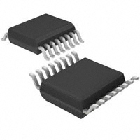
The LT®1713/LT1714 are UltraFastTM 7ns, single/dual comparators featuring rail-to-rail inputs, rail-to-rail complementary outputs and an output latch. Optimized for 3V and 5V power supplies, they operate over a single supply voltage range from 2.4V to 12V or from ±2.4V to ± 6V dual supplies. The LT1713/LT1714 are designed for ease of use in a variety of systems. In addition to wide supply voltage flexibility, rail-to-rail input common mode range extends 100mV beyond both supply rails and the outputs are protected against phase reversal for inputs extending further beyond the rails. Also, the rail-to-rail inputs may be taken to opposite rails with no significant increase in input current. The rail-to-rail matched complementary outputs interface directly to TTL or CMOS logic and can sink 10mA to within 0.5V of GND or source 10mA to within 0.7V of V +. The LT1713/LT1714 have internal TTL/CMOS compatible latches for retaining data at the outputs. Each latch holds data as long as its latch pin is held high. Latch pin hysteresis provides protection against slow moving or noisy latch signals. The LT1713 is available in the 8-lead MSOP package. The LT1714 is available in the 16-lead narrow SSOP package.
, LTC and LT are registered trademarks of Linear Technology Corporation. UltraFast is a trademark of Linear Technology Corporation.
s s s s s s
Ultrafast: 7ns at 20mV Overdrive 8.5ns at 5mV Overdrive Rail-to-Rail Inputs Rail-to-Rail Complementary Outputs (TTL/CMOS Compatible) Specified at 2.7V, 5V and ±5V Supplies Low Power (Per Comparator): 5mA Output Latch Inputs Can Exceed Supplies Without Phase Reversal LT1713: 8-Lead MSOP Package LT1714: 16-Lead Narrow SSOP Package
APPLICATIO S
s s s s s s s s s s s
High Speed Automatic Test Equipment Current Sense for Switching Regulators Crystal Oscillator Circuits High Speed Sampling Circuits High Speed A/D Converters Pulse Width Modulators Window Comparators Extended Range V/F Converters Fast Pulse Height/Width Discriminators Line Receivers High Speed Triggers
TYPICAL APPLICATIO
A 4× NTSC Subcarrier Voltage-Tunable Crystal Oscillator
5V 1N4148 1M 5V 1M 2k 100pF MV-209 VARACTOR DIODE 1M* 47k* LT1004-2.5 3.9k* 1k*
PROPAGATION DELAY (ns)
VIN 0V TO 5V
1M
0.047µF C SELECT (CHOOSE FOR CORRECT PLL LOOP RESPONSE)
390Ω
+
LT1713
Y1** 15pF 100pF
–
2k 200pF
FREQUENCY OUTPUT
171314 TA01
* 1% FILM RESISTOR ** NORTHERN ENGINEERING LABS C-2350N-14.31818MHz
U
U
U
LT1713/LT1714 Propagation Delay vs Input Overdrive
9.0 8.5 8.0 7.5 7.0 6.5 6.0 5.5 5.0 0 10 20 40 50 30 INPUT OVERDRIVE (mV) 60 tPD– tPD+ TA = 25°C V + = 5V V – = 0V VSTEP = 100mV
171314 TA02
1
�LT1713/LT1714
ABSOLUTE
AXI U
RATI GS
Supply Voltage V + to V – ............................................................ 12.6V V + to GND ........................................................ 12.6V V – to GND .............................................– 10V to 0.3V Differential Input Voltage ................................... ± 12.6V Latch Pin Voltage ...................................................... 7V Input and Latch Current ..................................... ± 10mA
PACKAGE/ORDER I FOR ATIO
ORDER PART NUMBER
TOP VIEW V+ +IN –IN V– 1 2 3 4 8 7 6 5 Q OUT Q OUT GND LATCH ENABLE
LT1713CMS8 LT1713IMS8
MS8 PACKAGE 8-LEAD PLASTIC MSOP
MS8 PART MARKING LTRD LTUK
TJMAX = 150°C, θJA = 250°C/ W
Consult factory for parts specified with wider operating temperature ranges.
The q denotes specifications which apply over the full operating temperature range, otherwise specifications are at TA = 25°C. V + = 2.7V or V + = 5V, V – = 0V, VCM = V +/2, VLATCH = 0.8V, CLOAD = 10pF, VOVERDRIVE = 20mV, unless otherwise specified.
SYMBOL PARAMETER V+ VOS Positive Supply Voltage Range Input Offset Voltage (Note 4) RS = 50Ω, VCM = V +/2 RS = 50Ω, VCM = V +/2 (Note 11) RS = 50Ω, VCM = 0V RS = 50Ω, VCM = V + CONDITIONS
q q
ELECTRICAL CHARACTERISTICS
∆VOS/∆T IOS IB VCM CMRR
Input Offset Voltage Drift Input Offset Current
Input Bias Current (Note 5)
q
Input Voltage Range (Note 9) Common Mode Rejection Ratio V + = 5V, 0V ≤ VCM ≤ 5V V + = 5V, 0V ≤ VCM ≤ 5V V + = 2.7V, 0V ≤ VCM ≤ 2.7V V + = 2.7V, 0V ≤ VCM ≤ 2.7V
2
U
U
W
WW
U
W
(Note 1)
Output Current (Continuous) .............................. ± 20mA Operating Temperature Range ................ – 40°C to 85°C Specified Temperature Range (Note 2) ... – 40°C to 85°C Junction Temperature .......................................... 150°C Storage Temperature Range ................. – 65°C to 150°C Lead Temperature (Soldering, 10 sec).................. 300°C
TOP VIEW –IN A +IN A V– V+ V+ V
–
1 2 3 4 5 6 7 8
LATCH ENABLE A 15 GND 16 14 Q A 13 Q A 12 Q B 11 Q B 10 GND LATCH 9 ENABLE B
ORDER PART NUMBER LT1714CGN LT1714IGN
+IN B –IN B
GN PART MARKING 1714 1714I
GN PACKAGE 16-LEAD PLASTIC SSOP
TJMAX = 150°C, θJA = 120°C/ W
MIN 2.4
TYP 0.5 0.7 1
MAX 7 4 5
UNITS V mV mV mV mV µV/°C µA µA µA µA V dB dB dB dB
q q
5 0.1 –7 – 15 – 0.1 60 58 57 55 70 70 – 1.5 1 2 2 5 V + + 0.1
q q q
�LT1713/LT1714
ELECTRICAL CHARACTERISTICS
The q denotes specifications which apply over the full operating temperature range, otherwise specifications are at TA = 25°C. V + = 2.7V or V + = 5V, V – = 0V, VCM = V +/2, VLATCH = 0.8V, CLOAD = 10pF, VOVERDRIVE = 20mV, unless otherwise specified.
SYMBOL PARAMETER PSRR+ PSRR– AV VOH VOL I+ I– VIH VIL IIL tPD Positive Power Supply Rejection Ratio Negative Power Supply Rejection Ratio Small-Signal Voltage Gain (Note 10) Output Voltage Swing HIGH Output Voltage Swing LOW Positive Supply Current (Per Comparator) Negative Supply Current (Per Comparator) Latch Pin High Input Voltage Latch Pin Low Input Voltage Latch Pin Current Propagation Delay (Note 6) VLATCH = V+ ∆VIN = 100mV, VOVERDRIVE = 20mV ∆VIN = 100mV, VOVERDRIVE = 20mV ∆VIN = 100mV, VOVERDRIVE = 5mV ∆VIN = 100mV, VOVERDRIVE = 20mV 10% to 90% 90% to 10% IOUT OVERDRIVE = 50mV IOUT = 10mA, V + = 5V, VOVERDRIVE = 50mV IOUT = – 1mA, VOVERDRIVE = 50mV IOUT = – 10mA, VOVERDRIVE = 50mV V + = 5V, VOVERDRIVE = 1V
q
CONDITIONS 2.4V ≤ V + ≤ 7V, VCM = 0V
q
MIN 65 60 65 60 1.5
TYP 80 80 3 V + – 0.2 V + – 0.4 0.20 0.35 5 3
MAX
UNITS dB dB dB dB V/mV V V
– 7V ≤ V – ≤ 0V, V + = 5V, VCM = 5V
q
= 1mA, V + = 5V, V
q V + – 0.5 q V + – 0.7 q q
0.4 0.5 6.5 8.0 4.0 4.5 0.8 10
V V mA mA mA mA V V µA ns ns ns ns ns ns ns ns ns ns MHz psRMS
V + = 5V, VOVERDRIVE = 1V
q q q q
2.4
8.0
q
11.0 12.5 3
9.0 0.5 4 4 8 1.5 0 8
∆tPD tr tf tLPD tSU tH tDPW fMAX tJITTER
Differential Propagation Delay (Note 6) Output Rise Time Output Fall Time Latch Propagation Delay (Note 7) Latch Setup Time (Note 7) Latch Hold Time (Note 7) Minimum Latch Disable Pulse Width (Note 7) Maximum Toggle Frequency Output Timing Jitter
VIN = 100mVP-P Sine Wave VIN = 630mVP-P (0dBm) Sine Wave, f = 30MHz
65 15
The q denotes specifications which apply over the full operating temperature range, otherwise specifications are at TA = 25°C. V + = 5V, V – = – 5V, VCM = 0V, VLATCH = 0.8V, CLOAD = 10pF, VOVERDRIVE = 20mV, unless otherwise specified.
SYMBOL PARAMETER V+ V– VOS Positive Supply Voltage Range Negative Supply Voltage Range (Note 3) Input Offset Voltage (Note 4) RS = 50Ω, VCM = 0V RS = 50Ω, VCM = 0V RS = 50Ω, VCM = – 5V RS = 50Ω, VCM = 5V CONDITIONS
q q q
MIN 2.4 –7
TYP
MAX 7 0
UNITS V V mV mV mV mV µV/°C µA µA µA µA
0.5 0.7 1
q q
3 4
∆VOS/∆T IOS IB
Input Offset Voltage Drift Input Offset Current Input Bias Current (Note 5)
5 0.1 –7 – 15 – 1.5 1 2 2 5
q
3
�LT1713/LT1714
ELECTRICAL CHARACTERISTICS
SYMBOL PARAMETER VCM CMRR PSRR+ PSRR– AV VOH VOL I+ I– VIH VIL IIL tPD Input Voltage Range Common Mode Rejection Ratio Positive Power Supply Rejection Ratio Negative Power Supply Rejection Ratio Small-Signal Voltage Gain (Note 10) Output Voltage Swing HIGH (Note 8) Output Voltage Swing LOW (Note 8) Positive Supply Current (Per Comparator) Negative Supply Current (Per Comparator) Latch Pin High Input Voltage Latch Pin Low Input Voltage Latch Pin Current Propagation Delay (Note 6)
The q denotes specifications which apply over the full operating temperature range, otherwise specifications are at TA = 25°C. V + = 5V, V – = – 5V, VCM = 0V, VLATCH = 0.8V, CLOAD = 10pF, VOVERDRIVE = 20mV, unless otherwise specified.
CONDITIONS
q
MIN – 5.1 62 60 68 65 65 60 1.5
q q q q q
TYP 70 80 80 3 4.8 4.6 0.20 0.35 5.5 3.5
MAX 5.1
UNITS V dB dB dB dB dB dB V/mV V V
– 5V ≤ VCM ≤ 5V
q
2.4V ≤ V +
≤ 7V, VCM = – 5V
q
– 7V ≤ V – ≤ 0V, VCM = 5V
q
1V ≤ VOUT ≤ 4V, RL = ∞ IOUT = 1mA, VOVERDRIVE = 50mV IOUT = 10mA, VOVERDRIVE = 50mV IOUT = – 1mA, VOVERDRIVE = 50mV IOUT = – 10mA, VOVERDRIVE = 50mV VOVERDRIVE = 1V VOVERDRIVE = 1V
q q q
4.5 4.3
0.4 0.5 7.5 9.0 4.5 5.0 0.8 10
V V mA mA mA mA V V µA ns ns ns ns ns ns ns ns ns ns MHz psRMS
2.4
VLATCH = V + ∆VIN = 100mV, VOVERDRIVE = 20mV ∆VIN = 100mV, VOVERDRIVE = 20mV ∆VIN = 100mV, VOVERDRIVE = 5mV ∆VIN = 100mV, VOVERDRIVE = 20mV 10% to 90% 90% to 10%
q
7
q
10 12 3
8.5 0.5 4 4 8 1.5 0 8
∆tPD tr tf tLPD tSU tH tDPW fMAX tJITTER
Differential Propagation Delay (Note 6) Output Rise Time Output Fall Time Latch Propagation Delay (Note 7) Latch Setup Time (Note 7) Latch Hold Time (Note 7) Minimum Latch Disable Pulse Width (Note 7) Maximum Toggle Frequency Output Timing Jitter
VIN = 100mVP-P Sine Wave VIN = 630mVP-P (0dBm) Sine Wave, f = 30MHz
65 15
Note 1: Absolute Maximum Ratings are those values beyond which the life of a device may be impaired. Note 2: The LT1713C/LT1714C are guaranteed to meet specified performance from 0°C to 70°C. They are designed, characterized and expected to meet specified performance from – 40°C to 85°C but are not tested or QA sampled at these temperatures. The LT1713I/LT1714I are guaranteed to meet specified performance from – 40°C to 85°C. Note 3: The negative supply should not be greater than the ground pin voltages and the maximum voltage across the positive and negative supplies should not be greater than 12V. Note 4: Input offset voltage (VOS) is defined as the average of the two voltages measured by forcing first one output, then the other to V +/2. Note 5: Input bias current (IB) is defined as the average of the two input currents.
Note 6: Propagation delay (tPD) is measured with the overdrive added to the actual VOS. Differential propagation delay is defined as: ∆tPD = tPD+ – tPD–. Load capacitance is 10pF. Due to test system requirements, the LT1713/LT1714 propagation delay is specified with a 1kΩ load to ground for ± 5V supplies, or to mid-supply for 2.7V or 5V single supplies. Note 7: Latch propagation delay (tLPD) is the delay time for the output to respond when the latch pin is deasserted. Latch setup time (tSU) is the interval in which the input signal must remain stable prior to asserting the latch signal. Latch hold time (tH) is the interval after the latch is asserted in which the input signal must remain stable. Latch disable pulse width (tDPW) is the width of the negative pulse on the latch enable pin that latches in new data on the data inputs.
4
�LT1713/LT1714
ELECTRICAL CHARACTERISTICS
Note 8: Output voltage swings are characterized and tested at V + = 5V and V – = 0V. They are designed and expected to meet these same specifications at V – = – 5V. Note 9: The input voltage range is tested under the more demanding conditions of V + = 5V and V – = – 5V. The LT1713/LT1714 are designed and expected to meet these specifications at V – = 0V. Note 10: The LT1713/LT1714 voltage gain is tested at V + = 5V and V – = – 5V only. Voltage gain at single supply V + = 5V and V + = 2.7V is guaranteed by design and correlation. Note 11: Input offset voltage over temperature at V + = 2.7V is guaranteed by design and characterization.
TYPICAL PERFOR A CE CHARACTERISTICS
Input Offset Voltage vs Temperature
2.5 2.0 V+ = 5V V – = 0V VCM = 2.5V
PROPAGATION DELAY (ns)
INPUT OFFSET VOLTAGE (mV)
PROPAGATION DELAY (ns)
1.5 1.0 0.5 0 – 0.5 – 1.0 – 1.5 – 2.0
– 2.5 –50
–25
50 0 75 25 TEMPERATURE (°C)
POSITIVE SUPPLY CURRENT (PER COMPARATOR) (mA)
Propagation Delay vs Input Common Mode Voltage
10.0 9.5
PROPAGATION DELAY (ns)
PROPAGATION DELAY (ns)
9.0 8.5 tPD 8.0 7.5 7.0 6.5 6.0 – 0.5 0.5 1.5 tPD– TA = 25°C V + = 5V V – = 0V VOD = 20mV VSTEP = 100mV CLOAD = 10pF 3.5 4.5 2.5 INPUT COMMON MODE (V) 5.5
+
UW
100
171314 G01
Propagation Delay vs Load Capacitance
14 12 10 8 6 4 2 0 0 TA = 25°C V + = 5V V – = 0V VCM = 2.5V VOD = 20mV VSTEP = 100mV 20 80 60 100 40 LOAD CAPACITANCE (pF) 120 tPD– tPD+ 16 14 12 10 8 6 4 2
Propagation Delay vs Temperature
V+ = 5V V – = 0V VCM = 2.5V VOD = 20mV VSTEP = 100mV CLOAD = 10pF tPD+ tPD–
125
0 –50 –25
0
25
50
75
100
125
TEMPERATURE (°C)
171314 G03
171314 G02
Propagation Delay vs Positive Supply Voltage
10.0 9.5 9.0 8.5 8.0 7.5 7.0 6.5 6.0 0 2 10 12 8 6 POSITIVE SUPPLY VOLTAGE (V) 4 14 TA = 25°C V – = 0V VCM = 2.5V VOD = 20mV VSTEP = 100mV CLOAD = 10pF
Positive Supply Current vs Positive Supply Voltage
7.0 TA = 25°C ∆VIN = 100mV 6.5 IOUT = 0 V – = – 5V 6.0 V – = 0V 5.5 5.0 4.5 4.0
tPD+
tPD–
2
6 8 10 4 POSITIVE SUPPLY VOLTAGE (V)
12
171314 G06
171314 G04
171314 G05
5
�LT1713/LT1714 TYPICAL PERFOR A CE CHARACTERISTICS
POSITIVE SUPPLY CURRENT (PER COMPARATOR) (mA)
NEGATIVE SUPPLY CURRENT (PER COMPARATOR) (mA)
Positive Supply Current vs Switching Frequency
40 TA = 25°C + 35 V – = 5V V = 0V 30 CLOAD = 10pF 25 20 15 10 5 0 0 20 10 30 SWITCHING FREQUENCY (MHz) 40
3.4 3.2 3.0 2.8 2.6 2.4 2.2 2.0 0
V + = 5V
INPUT BIAS CURRENT (µA)
Input Bias Current vs Temperature
0 V+ = 5V V – = 0V VCM = 2.5V
OUTPUT VOLTAGE (V)
INPUT BIAS CURRENT (µA)
4.7 4.6 4.5 4.4 4.3 T = 25°C 4.2 VA = 5V + – 4.1 V = 0V ∆VIN = 100mV 4.0 1 0.01 0.1 LOADING SOURCE CURRENT (mA)
OUTPUT VOLTAGE (V)
–1
–2
–3
–4 –50 –25
0
25
50
75
TEMPERATURE (°C)
171314 G10
Output Timing Jitter vs Switching Frequency
200 180
OUTPUT TIMING JITTER (psRMS)
160 140 120 100 80 60 40 20 0 0 20
TA = 25°C V + = 5V V – = 0V VCM = 2.5V VIN = 630mVP-P (0dBm) SINE WAVE
40 60 FREQUENCY (MHz)
6
UW
171314 G07
Negative Supply Current vs Negative Supply Voltage
4.0 3.8 3.6 TA = 25°C ∆VIN = 100mV IOUT = 0
Input Bias Current vs Input Common Mode Voltage
3 2 1 0 –1 –2 –3 –4 –5 –6 TA = 25°C V + = 5V V – = 0V ∆VIN = 0mV
V + = 2.7V
–3 –4 –2 –5 –6 –1 NEGATIVE SUPPLY VOLTAGE (V)
–7
–1
1 2 0 3 4 5 INPUT COMMON MODE VOLTAGE (V)
6
171314 G08
171314 G09
Output High Voltage vs Source Current
5.0 4.9 4.8 1.0 0.9 0.8 0.7 0.6 0.5 0.4 0.3 0.2 0.1 10
Output Low Voltage vs Sink Current
TA = 25°C V + = 5V V – = 0V ∆VIN = 100mV
100
125
0 0.01
1 0.1 LOADING SINK CURRENT (mA)
10
171314 G12
171314 G11
Output Rising Edge, 5V Supply
Output Falling Edge, 5V Supply
VIN
VIN
VOUT
VOUT
171314 G14
171314 G15
80
171314 G13
�LT1713/LT1714
PI FU CTIO S
LT1713 V + (Pin 1): Positive Supply Voltage, Usually 5V. + IN (Pin 2): Noninverting Input. – IN (Pin 3): Inverting Input. V – (Pin 4): Negative Supply Voltage, Usually 0V or – 5V. LATCH ENABLE (Pin 5): Latch Enable Input. With a logic high the output is latched. GND (Pin 6): Ground Supply Voltage, Usually 0V. Q (Pin 7): Noninverting Output. Q (Pin 8): Inverting Output.
LT1714 – IN A (Pin 1): Inverting Input of A Channel Comparator. + IN A (Pin 2): Noninverting Input of A Channel Comparator. V – (Pins 3, 6): Negative Supply Voltage, Usually – 5V. Pins 3 and 6 should be connected together externally. V + (Pins 4, 5): Positive Supply Voltage, Usually 5V. Pins 4 and 5 should be connected together externally. + IN B (Pin 7): Noninverting Input of B Channel Comparator. – IN B (Pin 8): Inverting Input of B Channel Comparator. LATCH ENABLE B (Pin 9): Latch Enable Input of B Channel Comparator. With a logic high, the B output is latched. GND (Pin 10): Ground Supply Voltage of B Channel Comparator, Usually 0V. Q B (Pin 11): Noninverting Output of B Channel Comparator. Q B (Pin 12): I nverting Output of B Channel Comparator. Q A (Pin 13): I nverting Output of A Channel Comparator. Q A (Pin 14): Noninverting Output of A Channel Comparator. GND (Pin 15): Ground Supply Voltage of A Channel Comparator, Usually 0V LATCH ENABLE A (Pin 16): Latch Enable Input of A Channel Comparator. With a logic high, the A output is latched.
U
U
U
7
�LT1713/LT1714
APPLICATIO S I FOR ATIO
Common Mode Considerations
The LT1713/LT1714 are specified for a common mode range of – 5.1V to 5.1V on a ± 5V supply, or a common mode range of – 0.1V to 5.1V on a single 5V supply. A more general consideration is that the common mode range is from 100mV below the negative supply to 100mV above the positive supply, independent of the actual supply voltage. The criteria for common mode limit is that the output still responds correctly to a small differential input signal. When either input signal falls outside the common mode limit, the internal PN diode formed with the substrate can turn on resulting in significant current flow through the die. Schottky clamp diodes between the inputs and the supply rails speed up recovery from excessive overdrive conditions by preventing these substrate diodes from turning on. Input Bias Current Input bias current is measured with the outputs held at 2.5V with a 5V supply voltage. As with any rail-to-rail differential input stage, the LT1713/LT1714 bias current flows into or out of the device depending upon the common mode level. The input circuit consists of an NPN pair and a PNP pair. For inputs near the negative rail, the NPN pair is inactive, and the input bias current flows out of the device; for inputs near the positive rail, the PNP pair is inactive, and these currents flow into the device. For inputs far enough away from the supply rails, the input bias current will be some combination of the NPN and PNP bias currents. As the differential input voltage increases, the input current of each pair will increase for one of the inputs and decrease for the other input. Large differential input voltages result in different input currents as the input stage enters various regions of operation. To reduce the influence of these changing input currents on system operation, use a low source resistance.
8
U
Latch Pin Dynamics The internal latches of the LT1713/LT1714 comparators retain the input data (output latched) when their respective latch pin goes high. The latch pin will float to a low state when disconnected, but it is better to ground the latch when a flow-through condition is desired. The latch pin is designed to be driven with either a TTL or CMOS output. It has built-in hysteresis of approximately 100mV, so that slow moving or noisy input signals do not impact latch performance. For the LT1714, if only one of the comparators is being used at a given time, it is best to latch the second comparator to avoid any possibility of interactions between the two comparators in the same package. High Speed Design Techniques A substantial amount of design effort has made the LT1713/LT1714 relatively easy to use. As with most high speed comparators, careful attention to PC board layout and design is important in order to prevent oscillations. The most common problem involves power supply bypassing which is necessary to maintain low supply impedance. Resistance and inductance in supply wires and PC traces can quickly build up to unacceptable levels, thereby allowing the supply voltages to move as the supply current changes. This movement of the supply voltages will often result in improper operation. In addition, adjacent devices connected through an unbypassed supply can interact with each other through the finite supply impedances. Bypass capacitors furnish a simple solution to this problem by providing a local reservoir of energy at the device, thus keeping supply impedance low. Bypass capacitors should be as close as possible to the LT1713/LT1714 supply pins. A good high frequency capacitor, such as a 0.1µF ceramic, is recommended in parallel with a larger capacitor, such as a 4.7µF tantalum.
W
UU
�LT1713/LT1714
APPLICATIO S I FOR ATIO
Poor trace routes and high source impedances are also common sources of problems. Keep trace lengths as short as possible and avoid running any output trace adjacent to an input trace to prevent unnecessary coupling. If output traces are longer than a few inches, provide proper termination impedances (typically 100Ω to 400Ω) to eliminate any reflections that may occur. Also keep source impedances as low as possible, preferably much less than 1kΩ. The input and output traces should also be isolated from one another. Power supply traces can be used to achieve
Figure 1. Typical LT1714 Topside Metal for Multilayer PCB Layout
U
this isolation as shown in Figure 1, a typical topside layout of the LT1713/LT1714 on a multilayer PC board. Shown is the topside metal etch including traces, pin escape vias and the land pads for a GN16 LT1713/LT1714 and its adjacent X7R 0805 bypass capacitors. The V +, V – and GND traces all shield the inputs from the outputs. Although the two V – pins are connected internally, they should be shorted together externally as well in order for both to function as shields. The same is true for the two V + pins. The two GND pins are not connected internally, but in most applications they are both connected directly to the ground plane.
1714 F01
W
UU
9
�LT1713/LT1714
APPLICATIO S I FOR ATIO
Hysteresis
Another useful technique to avoid oscillations is to provide positive feedback, also known as hysteresis, from the output to the input. Increased levels of hysteresis, however, reduce the sensitivity of the device to input voltage levels, so the amount of positive feedback should be tailored to particular system requirements. The
Q VIN
+
LT1713 VIN
50Ω
–
50k 50Ω Q V + = 5V V – = – 5V VHYST = 5mV (ALL 3 CASES) VREF
Figure 2. Various Configurations for Introducing Hysteresis
10
U
LT1713/LT1714 are completely flexible regarding the application of hysteresis, due to rail-to-rail inputs and the complementary outputs. Specifically, feedback resistors can be connected from one or both outputs to their corresponding inputs without regard to common mode considerations. Figure 2 shows several configurations.
50k Q 50Ω 100k Q
W
UU
+
LT1713
VIN+ VIN– Q
+
LT1713
–
50Ω
–
Q 100k
171314 F02
�LT1713/LT1714
TYPICAL APPLICATIO S
Simultaneous Full Duplex 75Mbaud Interface with Only Two Wires The circuit of Figure 3 shows a simple, fully bidirectional, differential 2-wire interface that gives good results to 75Mbaud, using the LT1714. Eye diagrams under conditions of unidirectional and bidirectional communication are shown in Figures 4 and 5. Although not as pristine as the unidirectional performance of Figure 4, the performance under simultaneous bidirectional operation is still excellent. Because the LT1714 input voltage range extends 100mV beyond both supply rails, the circuit works with a full ± 3V (one whole VS up or down) of ground potential difference. The circuit works well with the resistor values shown, but other sets of values can be used. The starting point is the characteristic impedance, ZO, of the twisted-pair cable. The input impedance of the resistive network should match the characteristic impedance and is given by:
750k 3V 4 14 RxD 3V
+ –
15
2
1/2 LE LT1714 13 16 3
1
750k 100k 3V 49.9Ω TxD 7 R2A 2.55k 11 R3A 124Ω R3B 124Ω R2B 2.55k ROA 140Ω R1B 499Ω R1A 499Ω
+
5
49.9Ω
8
1/2 LT1714 – LE 10 12 6 9
100k
U
RIN = 2 • RO •
R1||(R2 + R3) RO + 2 • [R1||(R2 + R3)]
This comes out to 120Ω for the values shown. The Thevenin equivalent source voltage is given by:
VTH = VS • (R2 + R3 – R1) (R2 + R3 + R1) RO • RO + 2 • [R1||(R2 + R3)]
750k
2
+ –
3
4 14 RxD
1
1/2 LT1714 LE 15 16 13
3V
3V R1C 499Ω ROB 140Ω 6-FEET TWISTED PAIR ZO ≈ 120Ω DIODES: BAV99 ×4 R1D 499Ω R2C 2.55k
750k 100k 3V 5 11 R3C 124Ω R3D 124Ω R2D 2.55k
+
7
49.9Ω TxD
1/2 LT1714 8 LE – 12 6 10 9
49.9Ω
100k
171314 F03
Figure 3. 75Mbaud Full Duplex Interface on Two Wires
11
�LT1713/LT1714
TYPICAL APPLICATIO S
Figure 4. Performance of Figure 3’s Circuit When Operated Unidirectionally. Eye is Wide Open
This amounts to an attenuation factor of 0.0978 with the values shown. (The actual voltage on the lines will be cut in half again due to the 120Ω ZO.) The reason this attenuation factor is important is that it is the key to deciding the ratio between the R2-R3 resistor divider in the receiver path. This divider allows the receiver to reject the large signal of the local transmitter and instead sense the attenuated signal of the remote transmitter. Note that in the above equations, R2 and R3 are not yet fully determined because they only appear as a sum. This allows the designer to now place an additional constraint on their values. The R2-R3 divide ratio should be set to equal half the attenuation factor mentioned above or: R3/R2 = 1/2 • 0.09761. Having already designed R2 + R3 to be 2.653k (by allocating input impedance across RO, R1 and R2 + R3 to get the requisite 120Ω), R2 and R3 then become 2529Ω and 123.5Ω respectively. The nearest 1% value for R2 is 2.55k and that for R3 is 124Ω. Voltage-Tunable Crystal Oscillator The front page application is a variant of a basic crystal oscillator that permits voltage tuning of the output frequency. Such voltage-controlled crystal oscillators (VCXO) are often employed where slight variation of a stable carrier is required. This example is specifically intended to provide a 4 × NTSC sub-carrier tunable oscillator suitable for phase locking.
FREQUENCY DEVIATION (kHz)
12
U
171112 F04
171112 F05
Figure 5. Performance When Operated Simultaneous Bidirectionally (Full Duplex). Crosstalk Appears as Noise. Eye is Slightly Shut But Performance is Still Excellent
The LT1713 is set up as a crystal oscillator. The varactor diode is biased from the tuning input. The tuning network is arranged so a 0V to 5V drive provides a reasonably symmetric, broad tuning range around the 14.31818MHz center frequency. The indicated selected capacitor sets tuning bandwidth. It should be picked to complement loop response in phase locking applications. Figure 6 is a plot of tuning input voltage versus frequency deviation. Tuning deviation from the 4 × NTSC 14.31818MHz center frequency exceeds ± 240ppm for a 0V to 5V input.
1
Using the design value of R2 + R3 = 2.653k rather than the implementation value of 2.55k + 124Ω = 2.674k.
9 8 7 6 5 4 3 2 1 14.314.0MHz 0 0 1 14.31818MHz
14.3217MHz
3 2 INPUT VOLTAGE (V)
4
171112 F06
5
Figure 6. Control Voltage vs Output Frequency for the First Page Application Circuit. Tuning Deviation from Center Frequency Exceeds ± 240ppm
�LT1713/LT1714
TYPICAL APPLICATIO S
1MHz Series Resonant Crystal Oscillator with Square and Sinusoid Outputs Figure 7 shows a classic 1MHz series resonant crystal oscillator. At series resonance, the crystal is a low impedance and the positive feedback connection is what brings about oscillation at the series resonant frequency. The RC feedback around the other path ensures that the circuit does not find a stable DC operating point and refuse to oscillate. The comparator output is a 1MHz square wave (top trace of Figure 8) with jitter measured at better than 28psRMS on a 5V supply and 40psRMS on a 3V supply. At Pin 2 of the comparator, on the other side of the crystal, is a clean sine wave except for the presence of the small high frequency glitch (middle trace of Figure 8). This glitch is caused by the fast edge of the comparator output feeding back through crystal capacitance. Amplitude stability of the sine wave is maintained by the fact that the sine wave is basically a filtered version of the square wave. Hence, the usual amplitude control loops associated with sinusoidal oscillators are not necessary.2 The sine wave is filtered and buffered by the fast, low noise LT1806 op amp. To remove the glitch, the LT1806 is configured as a bandpass filter with a Q of 5 and unity-gain center frequency of 1MHz, with its output shown as the bottom trace of Figure 8. Distortion was measured at – 70dBc and – 60dBc on the second and third harmonics, respectively.
2
VS R1 1k R2 1k
2
+ –
3
C1 0.1µF
Figure 7. LT1713 Comparator is Configured as a Series Resonant Xtal Oscillator. LT1806 Op Amp is Configured in a Q = 5 Bandpass with fC = 1MHz
Figure 8. Oscillator Waveforms with VS = 3V. Top is Comparator Output. Middle is Xtal Feedback to Pin 2 at LT1713 (Note the Glitches). Bottom is Buffered, Inverted and Bandpass Filtered with a Q = 5 by LT1806
U
6
Amplitude will be a linear function of comparator output swing, which is supply dependent and therefore adjustable. The important difference here is that any added amplitude stabilization or control loop will not be faced with the classical task of avoiding regions of nonoscillation versus clipping.
R10 1k 1MHz AT-CUT R4 210Ω VS 1 7 LT1713 LE 5
R5 6.49k C5 100pF R6 162Ω C3 100pF
C4 100pF
VS 2
R7 15.8k 6 1
– +
7 LT1806 SINE
R9 2k SQUARE 8 R3 1k VS C2 0.1µF
3 R8 2k
4
171314 F07
4
3V/DIV
1V/DIV
1V/DIV
200ns/DIV
171112 F08
13
�LT1713/LT1714
PACKAGE DESCRIPTIO U
Dimensions in inches (millimeters) unless otherwise noted.
MS8 Package 8-Lead Plastic MSOP
(LTC DWG # 05-08-1660)
0.118 ± 0.004* (3.00 ± 0.102)
8
76
5
0.193 ± 0.006 (4.90 ± 0.15)
0.118 ± 0.004** (3.00 ± 0.102)
1 0.043 (1.10) MAX 0.007 (0.18) 0.021 ± 0.006 (0.53 ± 0.015) 0° – 6° TYP SEATING PLANE
23
4 0.034 (0.86) REF
0.009 – 0.015 (0.22 – 0.38)
0.0256 (0.65) BSC
0.005 ± 0.002 (0.13 ± 0.05)
MSOP (MS8) 1100
* DIMENSION DOES NOT INCLUDE MOLD FLASH, PROTRUSIONS OR GATE BURRS. MOLD FLASH, PROTRUSIONS OR GATE BURRS SHALL NOT EXCEED 0.006" (0.152mm) PER SIDE ** DIMENSION DOES NOT INCLUDE INTERLEAD FLASH OR PROTRUSIONS. INTERLEAD FLASH OR PROTRUSIONS SHALL NOT EXCEED 0.006" (0.152mm) PER SIDE
14
�LT1713/LT1714
PACKAGE DESCRIPTIO U
Dimensions in inches (millimeters) unless otherwise noted. GN Package 16-Lead Plastic SSOP (Narrow 0.150)
(LTC DWG # 05-08-1641)
0.189 – 0.196* (4.801 – 4.978) 16 15 14 13 12 11 10 9
0.009 (0.229) REF
0.229 – 0.244 (5.817 – 6.198)
0.150 – 0.157** (3.810 – 3.988)
1 0.015 ± 0.004 × 45° (0.38 ± 0.10) 0.007 – 0.0098 (0.178 – 0.249) 0.016 – 0.050 (0.406 – 1.270) * DIMENSION DOES NOT INCLUDE MOLD FLASH. MOLD FLASH SHALL NOT EXCEED 0.006" (0.152mm) PER SIDE ** DIMENSION DOES NOT INCLUDE INTERLEAD FLASH. INTERLEAD FLASH SHALL NOT EXCEED 0.010" (0.254mm) PER SIDE 0° – 8° TYP 0.053 – 0.068 (1.351 – 1.727)
23
4
56
7
8 0.004 – 0.0098 (0.102 – 0.249)
0.008 – 0.012 (0.203 – 0.305)
0.0250 (0.635) BSC
GN16 (SSOP) 1098
TYPICAL APPLICATIO
Rail-to-Rail Pulse Width Modulator Using the LT1714 Binary modulation schemes are used in order to improve efficiency and reduce physical circuit size. They do this by reducing the power dissipation in the output driver transistors. In a normal Class A or Class AB amplifier, voltage drop and current flow exist simultaneously in the output transistors and power losses proportional to V • I occur. In a binary modulation scheme, the output transistors, whether bipolar or FET, are switched hard-on and hard-off so that voltage drops do not occur simultaneously with
Information furnished by Linear Technology Corporation is believed to be accurate and reliable. However, no responsibility is assumed for its use. Linear Technology Corporation makes no representation that the interconnection of its circuits as described herein will not infringe on existing patent rights.
U
current flow. The circuit of Figure 9 shows an example of a binary modulation scheme, in this case pulse width modulation. The LT1809 is configured as an integrator in order to generate nice linear rail-to-rail voltage ramps. The polarity of the ramp is determined by the output of the LT1714’s comparator A into R4. The heavy hysteresis of R1 around the LT1714’s comparator A combined with the feedback of the LT1809 force the devices to perpetually reverse each other, resulting in a 1MHz triangle wave. This constitutes the usual first half of any pulse width modulator, but the
15
�LT1713/LT1714
TYPICAL APPLICATIO
forte of this particular implementation is that it is rail-torail allowing a full-scale analog input. Once the triangle wave is achieved, the remainder of the pulse width modulator is easy, and is constituted by doing a simple comparison using the second half of the LT1714. The triangle wave and the relatively slow moving analog signal (the one to be modulated or to do the modulation, depending on how you look at it) are fed into the inputs of comparator B, whose output is then the PWM representation of the analog input voltage. The higher the analog input voltage, the wider the output pulse. The time averaged output level is thus proportional to the analog input voltage. This binary output can then be fed into power transistors with direct control over motor or speaker winding current, for
V+ R2 2k R3 2k
R1 26.1Ω V+ 2
+ –
4
A 1/2 LT1714 15 3
14
1
R4 13 499Ω
16 3 R5 1k
V+ V + = 2.7V TO 7V
RELATED PARTS
PART NUMBER LT1016 LT1116 LT1394 LT1671 LT1711/LT1712 LT1719 LT1720/LT1721 DESCRIPTION UltraFast Precision Comparator 12ns Single Supply Ground Sensing Comparator 7ns, UltraFast Single Supply Comparator 60ns, Low Power, Single Supply Comparator Single/Dual, 4.5ns, 3V/5V/±5V Rail-to-Rail Comparators 4.5ns, Single Supply 3V/5V Comparator Dual/Quad, 4.5ns, Single Supply Comparator COMMENTS Industry Standard 10ns Comparator Single Supply Version of the LT1016 6mA Single Supply Comparator 450µA Single Supply Comparator Faster Versions of LT1713/LT1714 4mA Comparator with Rail-to-Rail Outputs Dual/Quad Version of the LT1719
171314f LT/TP 0501 4K • PRINTED IN USA
16
Linear Technology Corporation
1630 McCarthy Blvd., Milpitas, CA 95035-7417
(408)432-1900 q FAX: (408) 434-0507 q www.linear-tech.com
U
example, with their inherent lowpass characteristic. Care must be taken to avoid cross conduction in the output power transistors. The linearity of the pulse width modulated signal can easily be ascertained by putting a simple 2-pole RC filter at the output (as shown in Figure 9). This demodulates the signal which can then be viewed and compared with the original input signal on an oscilloscope. Using a spectrum analyzer and a 1kHz reference signal, this circuit’s distortion products were measured as better than – 50dBc (0.3%) to about 3.5VP-P, degrading to – 30dBc (3%) as the circuit clips at 5VP-P on a single 5V supply.
C1 500pF ANALOG INPUT ANTIALIASING 1k FILTER C4 0.001µF 7 21Ω C3 100pF 1MHz TRIANGLE WAVE V+ 16kHz ANALOG FILTER FOR LINEARITY MEASUREMENT 11 12 1k C5 0.01µF 10k C6 0.001µF
171314 F09
2
1
V+ 7 6
+ –
5
–
LT1809
B 1/2 LT1714 9 6
8
10
+
R6 1k
4
C2 0.01µF
COMPLEMENTARY 1MHz PWM OUTPUTS
Figure 9. Rail-to-Rail 1MHz Pulse Width Modulator
© LINEAR TECHNOLOGY CORPORATION 2000
�