物料型号:
- LTC3539
- LTC3539-2
器件简介:
LTC3539/LTC3539-2是同步升压DC/DC转换器,能够提供高达2A的输出电流,分别以1MHz和2MHz的固定频率工作。这些转换器拥有输出断开功能,同步整流功能可实现高达94%的效率。它们在2mm×3mm DFN封装中工作,启动电压为700mV,能在低至500mV的电压下工作,从而延长电池寿命。
引脚分配:
- SW (Pin 1): 开关引脚,连接电感器和$V_{IN}$。
- PGND (Pin 2), GND (Pin 3): 信号和电源地。
- $VIN$ (Pin 4): 电池输入电压。
- SHDN (Pin 5): 逻辑控制的关闭输入。
- FB (Pin 6): 反馈输入到$g_{m}$误差放大器。
- MODE (Pin 7): 脉冲模式引脚,选择自动脉冲模式操作或强制固定频率操作。
- VOUT (Pin 8): 输出电压感测和内部同步整流器的漏极。
- Exposed Pad (Pin 9): 暴露的垫,必须焊接到PCB地平面。
参数特性:
- 输入电压范围:1.5V至5.25V
- 输出电压调整范围:1.5V至5.25V
- 反馈电压:1.170V至1.230V
- 待机电流:小于1μA
- 工作频率:LTC3539为1MHz,LTC3539-2为2MHz
功能详解:
- 从700mV电压启动,并在500mV下工作。
- 固定频率PWM设计,内部补偿,减少外部部件数量。
- 自动脉冲模式操作减少轻载条件下的功耗。
- 在不连续模式下通过阻尼电感器减少EMI。
- 具有低关闭电流和热过载保护。
应用信息:
- 医疗仪器、便携式条码扫描器、降噪耳机、便携GPS导航和手持PC等。
封装信息:
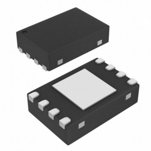
- LTC3539/LTC3539-2提供2mm×3mm×0.75mm的DFN封装。
- 所有引脚都与封装描述相关,并具有特定的功能。