Electrical Specifications Subject to Change
LTC3589 8-Output Regulator with Sequencing and I2C FEATURES
n n n n n n n n n n n n
DESCRIPTION
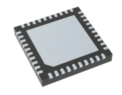
The LTC®3589 is a complete power management solution for ARM and ARM-based processors and advanced portable microprocessor systems. The device contains three synchronous step-down DC/DC converters for core, memory and SoC rails, a synchronous buck-boost regulator for I/O at 3.3V to 5V, and three 250mA LDO regulators for low noise analog supplies. An I2C serial port is used to control regulator enables, output voltage levels, dynamic voltage scaling and slew rate, operating modes and status reporting. Regulator start-up is sequenced by connecting regulator outputs to enable pins in the desired order or via the I2C port. System power-on, power-off and reset functions are controlled by pushbutton interface, pin inputs, or I2C interface. The LTC3589 supports i.MX, PXA and OMAP processors with eight independent rails at appropriate power levels, dynamic control and sequencing. Other features include interface signals such as the VSTB pin that toggles between programmed run and standby output voltages on up to four rails simultaneously. The device is available in a low profile 40-pin 6mm × 6mm exposed pad QFN package.
L, LT, LTC, LTM, Burst Mode, Linear Technology and the Linear logo are registered trademarks, Hot Swap and Bat-track are trademarks of Linear Technology Corporation. All other trademarks are the property of their respective owners.
Triple I2C Adjustable High Efficiency Step-Down Switching Regulators: 1.6A, 1A, 1A High Efficiency 1.2A Buck-Boost Switching Regulator Triple 250mA LDO Regulators Always Alive 25mA LDO Regulator Flexible Pin-Strap Sequencing Operation I2C and Independent Enable Control Pins Power Good and Reset Outputs Dynamic Voltage Scaling and Slew Rate Control Selectable 2.25MHz or 1.12MHz Switching Frequency Pushbutton ON/OFF Control with System Reset 10μA Standby Current 40-Pin 6mm × 6mm × 0.75mm QFN
APPLICATIONS
n n n n n n n
Handheld Instruments and Scanners Portable Industrial Devices Automotive Infotainment Portable Medical Devices High End Consumer Devices Multirail Systems Supports Freescale i.MX, Marvell PXA and Other Application Processors
TYPICAL APPLICATION
VRTC 1.2V AT 25mA MEMORY 0.9V TO 1.2V AT 250mA ANALOG 1.8V AT 250mA 1.8V, 2.5V, 2.8V, 3.3V AT 250mA VIN LDO1_STDBY
VIN 2.7V TO 5.5V
Start-Up Sequence
SW1 VCORE 0.6V TO 1.2V AT 1.6A I/O LDO2 LTC3589 SW2 VSRAM 0.9V TO 1.8V AT 1A VSOC 0.625V TO 1.25V AT 1A DDR MEMORY SW4AB SW4CD BB_OUT WAKE PBSTAT PGOOD GND RSTO
3589 TA01a
WAKE (1V/DIV) VSRAM ANALOG VSOC MEMORY VCORE I/O 3.3V AT 1.2A OR 5V AT 1A 500μs/DIV
3589 TA01b
LDO3
SW3
LDO4 3 I 7 ENABLES
2C
FROM μPROCESSOR
VSTB PWR_ON ON (PB)
HDD OR I/O
3589p
1
�LTC3589 TABLE OF CONTENTS
Features ............................................................................................................................ 1 Applications ....................................................................................................................... 1 Typical Application ............................................................................................................... 1 Description......................................................................................................................... 1 Absolute Maximum Ratings ..................................................................................................... 3 Pin Configuration ................................................................................................................. 3 Order Information ................................................................................................................. 3 Electrical Characteristics ........................................................................................................ 4 Typical Performance Characteristics .......................................................................................... 8 Pin Functions .....................................................................................................................12 Block Diagram....................................................................................................................14 Operation..........................................................................................................................15 Introduction .......................................................................................................................................................... 15 Always-On LDO..................................................................................................................................................... 16 250mA LDO Regulators ........................................................................................................................................ 16 Step-Down Switching Regulators ......................................................................................................................... 18 Buck-Boost Switching Regulator .......................................................................................................................... 22 Slewing DAC Reference Operation ........................................................................................................................ 26 Pushbutton Operation ........................................................................................................................................... 27 Enable and Power-On Sequencing ........................................................................................................................ 29 Fault Detection, Shutdown, and Reporting............................................................................................................ 30 I2C Operation ........................................................................................................................................................ 32 Thermal Considerations and Board Layout ........................................................................................................... 38 Applications Information .......................................................................................................40 Typical Application ..............................................................................................................42 Package Description ............................................................................................................43 Typical Application ..............................................................................................................44 Related Parts .....................................................................................................................44
3589p
2
�LTC3589 ABSOLUTE MAXIMUM RATINGS
(Notes 1, 3)
SW1, SW2, SW3, SW4AB, SW4CD (Transients < 1ms, Duty Cycle < 1%) ......................................... –0.3V to 7V PVIN1, PVIN2, PVIN3, PVIN4 ............... –0.3V to VIN + 0.3V VIN_LDO2, VIN_LDO34..........................–0.3V to VIN + 0.3V VIN, DVDD ..................................................... –0.3V to 6V LDO1_STBY, LDO1_FB, BUCK1_FB, BUCK2_FB, BUCK3_FB, BB_FB, BB_OUT, LDO2, LDO2_FB,LDO3, LDO4, PGOOD,
VSTB, EN1, EN2, EN3, EN4, EN_LDO2, EN_LDO34, ON, PBSTAT, WAKE, RSTO, PWR_ON, IRQ, ....... –0.3V to 6V SDA, SCL .....................................–0.3V to DVDD to 0.3V Operating Junction Temperature Range (Note 2).................................................. –40°C to 150°C Storage Temperature Range .................. –65°C to 150°C
PIN CONFIGURATION
TOP VIEW LDO1_STBY BUCK1_FB BUCK3_FB BUCK2_FB LDO2_FB LDO1_FB BB_FB
DVDD SW4CD
40 39 38 37 36 35 34 33 32 31 VIN_LDO2 1 LDO2 2 LDO3 3 LDO4 4 VIN_LD34 5 PVIN1 6 SW1 7 RSTO 8 EN_LDO2 9 EN1 10 11 12 13 14 15 16 17 18 19 20 PVIN4 BB_OUT IRQ EN_LDO34 PWR_ON EN2 SW4AB EN3 EN4 41 GND 30 SCL 29 PGOOD 28 VSTB 27 PVIN3 26 SW3 25 SW2 24 PVIN2 23 WAKE 22 PBSTAT 21 ON
UJ PACKAGE 40-LEAD (6mm × 6mm) PLASTIC QFN TJMAX = 125°C, θJA = 34°C/W EXPOSED PAD (PIN 41) IS GND, MUST BE SOLDERED TO PCB
ORDER INFORMATION
LEAD FREE FINISH LTC3589EUJ#PBF LTC3589IUJ#PBF LTC3589HUJ#PBF TAPE AND REEL LTC3589EUJ#TRPBF LTC3589IUJ#TRPBF LTC3589HUJ#TRPBF PART MARKING* 3589 3589 3589 PACKAGE DESCRIPTION 40-Lead (6mm × 6mm) Plastic QFN 40-Lead (6mm × 6mm) Plastic QFN 40-Lead (6mm × 6mm) Plastic QFN TEMPERATURE RANGE –40°C to 125°C –40°C to 125°C –40°C to 150°C
Consult LTC Marketing for parts specified with wider operating temperature ranges. *The temperature grade is identified by a label on the shipping container. Consult LTC Marketing for information on non-standard lead based finish parts. For more information on lead free part marking, go to: http://www.linear.com/leadfree/ For more information on tape and reel specifications, go to: http://www.linear.com/tapeandreel/
3589p
SDA
VIN
3
�LTC3589 ELECTRICAL CHARACTERISTICS
SYMBOL VIN IVINLDO1 fOSC IVIN PARAMETER Operating Input Supply Voltage, VIN VIN Quiescent Current Oscillator Frequency Pulse-Skipping Mode VIN Quiescent Current Per Buck Burst Mode ® VIN Quiescent Current Per Buck Feedback Pin Input Current Maximum Duty Cycle SW Pull-Down Resistance Soft-Start Rate Maximum Feedback Voltage Feedback LSB Step Size Minimum Feedback Voltage BxDTV1 = BxDTV2 = 00000, VIN = 2.7V to 5.5V
l
The l denotes the specifications which apply over the full operating junction temperature range, otherwise specifications are at TA = 25°C (Note 2). VIN = PVIN1 = PVIN2 = PVIN3 = PVIN4 = VIN_LDO2 = VIN_LDO34 = DVDD = 3.8V. All regulators disabled unless otherwise noted.
CONDITIONS
l
MIN 2.7
l l l l
TYP 10
MAX 5.5 17 2.6 TBD 40 0.1
UNITS V μA MHz μA μA μA % Ω V/ms
All Enables = 0V
1.9
2.25 135 27
Step Down Switching Regulators 1, 2, and 3 VFB = 0.85V (Note 5)
IFB DX RSW tSS VFB(MAX) VFB(LSB) VFB(MIN)
V FB = 0.8V VFB = 0V Regulators Disabled (Note 6) BxDTV1 = BxDTV2 = 11111, VIN = 2.7V to 5.5V
l
–0.1 100 2000 2 0.735 0.75 12.5 0.351 0.3625
0.765
V mV
0.374
V
1.6A Step Down Switching Regulator 1 (Buck 1) ILIM1 RP1 RN1 ILIM2, 3 RP2, 3 RN2, 3 IVIN VBB_FB VOUTBB ILIM4 IPEAK4 ILIMR4 IZERO4 RP4 RN4 ROUT4 tSS IFB Peak PMOS Current Limit SW1 RDS(ON) of PMOS1 RDS(ON) of NMOS1 Peak PMOS Current Limit SW2 RDS(ON) of PMOS3 RDS(ON) of NMOS3 PWM Mode VIN Quiescent Current Burst Mode VIN Quiescent Current Feedback Voltage Output Voltage Range Peak PMOS Current Limit SW4AB Forward Burst Current Limit (Switch A) Reverse Current Limit (Switch D) Reverse Burst Current Limit (Switch D) RDS(ON) of Switch A and Switch D RDS(ON) of Switch B and Switch C BB_OUT Pull-Down Resistance Soft-Start Rate Feedback Pin Input Current Burst Mode Operation ISW4AB = ISW4CD = 100mA ISW4AB = ISW4CD = –100mA Regulator Disabled (Note 6) V FB = 0.85V –0.1 Burst Mode Operation
l l
2.2
2.7 180 110
A mΩ mΩ A mΩ mΩ 130 19 μA μA V V A mA mA mA mΩ mΩ Ω V/ms 0.1 μA
ISW1 = 100mA ISW1 = 100mA
l
1.0A Step Down Switching Regulators 2 and 3 1.5 1.9 250 130 VBB_FB = 0.85V VIN = 2.7V to 5.5V, VOUT = 5.5V
l l l
1.2A Buck-Boost Switching Regulator 4 (Buck-Boost)
0.776 1.8 2.5
0.8 2.7 500 800 0 160 110 2000 2
0.824 5.0
3589p
4
�LTC3589 ELECTRICAL CHARACTERISTICS
SYMBOL tLDO_SS RLDO_PD PARAMETER Soft-Start Time LDO2, LDO3, LDO4 Output Pull-Down Resistance LDO2, LDO3, LDO4 LDO1 Feedback Voltage LDO1 Line Regulation LDO1 Load Regulation ILDO1 ILDO1_SC VDROP1 ILDO1_FB VIN_LDO2 IVIN_LDO2 IVIN VFB2(MAX) VFB2(LSB) VFB2(MIN) Available Output Current Short Circuit Output Current Limit Dropout Voltage (Note 4) LDO1_FB Input Current VIN_LDO2 Input Voltage Range VIN_LDO2 Quiescent Current VIN_LDO2 Shutdown Current VIN Quiescent Current LDO2 Maximum Feedback Voltage LDO2 Feedback LSB Step Size LDO2 Minimum Feedback Voltage L2DTV1 = L2DTV2 = 00000 VIN_LDO2 = VIN = 2.7V to 5.5V, ILDO2 = 1mA ILDO2 =1mA, VINLDO2 = 2.7V to 5.5V ILDO2 = 1mA to 250mA
l l
The l denotes the specifications which apply over the full operating junction temperature range, otherwise specifications are at TA = 25°C (Note 2). VIN = PVIN1 = PVIN2 = PVIN3 = PVIN4 = VIN_LDO2 = VIN_LDO34 = DVDD = 3.8V. All regulators disabled unless otherwise noted.
CONDITIONS MIN TYP 100 LDO Disabled 2000 MAX UNITS μs Ω
LDO Regulators
Always-On Regulator (LDO1_STDBY) VLDO1_FB VLDO1
l
0.76
0.8 0.2 0.2
0.84
V %/V % mA
ILDO1_STBY = 1mA, LDO1_STBY = 3.3V, VIN = 2.7V to 5.5V ILDO1 = 0.1mA to 25mA, LDO1_STBY = 3.3V
l
25 65 100 280 0.1 VIN 14 0 50 0.735 0.351 0.75 12.5 0.3625 0.373 19 1 80 0.765 180 –0.1
mA mV μA V μA μA μA V mV V
ILDO1 = 25mA, LDO1_STBY = 3.3V VLDO1_FB = 0.85V
l
LDO Regulator 2 (LDO2) 1.7 EN_LDO2 = High, LDO2_FB = 0.85V EN_LDO2 = Low EN_LDO2 = High L2DTV1 = L2DTV2 = 11111
l l l l
LDO2 Line Regulation LDO2 Load Regulation IOUT2 ISC2 VDROP2 ILDO2_FB VIN_LDO34 IVIN_LDO34 IVIN VLDO3 LDO2 Available Output Current LDO2 Short-Circuit Current Limit Dropout Voltage (Note 4) LDO2_FB Input Current VIN_LDO34 Input Range VIN_LDO34 Quiescent Current VIN_LDO34 Shutdown Current VIN Quiescent Current LDO3 Output Voltage LD03 Line Regulation LDO3 Load Regulation ILDO3 ILDO3_SC VDROP3 LDO3 Available Output Current LDO3 Short-Circuit Current Limit LDO3 Dropout Voltage (Note 4)
0.1 0.1 250 300 420 130 330 –0.1
l
%/V % mA 600 180 500 0.1 VIN mA mV mV μA V μA μA μA V %/V % mA 600 250 mA mV
ILDO2 = 200mA, VLDO2 = 2.5V ILDO2 = 200mA, VLDO2 = 1.2V VLDO2_FB = 0.8V
LDO Regulator 3 (LDO3) 2.35 14 0 50 1.746 1.8 0.1 0.1
l
EN_LDO3 = High, LDO3_FB = 0.85V Regulator Disabled VIN_LDO34 = VIN = 2.7V to 5V, ILDO3 = 1mA ILDO3 =1mA, VINLDO34 = 2.7V to 5.5V ILDO3 = 1mA to 250mA
l l l l
24 1 80 1.854
250 300 420 180
ILDO3 = 200mA, VLDO3 = 1.8V
3589p
5
�LTC3589 ELECTRICAL CHARACTERISTICS
SYMBOL VIN_LDO34 IVIN_LDO34 IVIN VLDO4 PARAMETER VIN_LDO34 Input Range VIN_LDO34 Quiescent Current VIN_LDO34 Shutdown Current Enabled VIN Quiescent Current LDO 4 Output Voltage ILDO4 = 1mA, L2DTV2[6:5] = 00 L2DTV2[6:5] = 01 L2DTV2[6:5] = 10 L2DTV2[6:5] = 11 ILDO4 =1mA, VINLDO4 = 2.7V to 5.5V, VOUT = 1.8V ILDO4 = 1mA to 250mA
l
The l denotes the specifications which apply over the full operating junction temperature range, otherwise specifications are at TA = 25°C (Note 2). VIN = PVIN1 = PVIN2 = PVIN3 = PVIN4 = VIN_LDO2 = VIN_LDO34 = DVDD = 3.8V. All regulators disabled unless otherwise noted.
CONDITIONS
l
MIN 2.35
TYP
MAX VIN
UNITS V μA μA μA V V V V %/V % mA
LDO Regulator 4 (LDO4) LDO4 Enabled, LDO4_FB = 0.85V LDO4 Disabled
l l l l l l l
14 0 50 2.716 2.245 1.746 3.201 2.8 2.5 1.8 3.3 0.1 0.1 250 300 420 100 180
22 1 80 2.884 2.575 1.854 3.399
LD04 Line Regulation LDO4 Load Regulation ILDO4 ILDO4_SC VDROP4 Enable Inputs VENx_THR VENx_THR2 VENx_THF2 RENX V VSTB_THR V VSTB_THF RVSTB VPWR_ONTHR VPWR_ONTHF RPWR_ON I2C Port DVDD IDVDD VDVDD_UVLO ADDRESS DVDD Input Supply Voltage DVDD Quiescent Current DVDD UVLO Level LTC3589 Device Address – Write LTC3589 Device Address – Read Threshold Rising, All Enables Low Threshold Rising, Any Enable High Threshold Falling, Any Enable High Input Pull-Down Resistance VSTB Pin Threshold Rising VSTB Pin Threshold Falling Pull-Down Resistence PWR_ON Pin Threshold Rising PWR_ON Pin Threshold Falling Pull-Down Resistence LDO4 Available Output Current LDO4 Short Circuit Current Limit LDO4 Dropout Voltage (Note 4)
600 130 250 1.2 0.525
mA mV mV V V V MΩ
ILDO4 = 200mA, VLDO4 = 3.3V ILDO4 = 200mA, VLDO4 = 1.8V
l l l
0.8 0.425 0.5 0.45 4.5
VSTB, PWR_ON Inputs
l l l l
0.4
0.8 0.7 4.5 0.8 0.7 4.5
1.2
V V MΩ V V MΩ
1.2
0.4
1.6 SCL/SDA = 0kHz 0.3 1 01101000 01101001 70
5.5
V μA V
VIH SDA, SCL SDA and SCL Input Threshold Rising VIL SDA, SCL SDA and SCL Input Threshold Falling IIHSCx IILSCx VOL SDA fSCL tBUF tHD_STA tSU_STA tSU_STO tHD_DAT(O) SDA and SCL Input Current SDA Output Low Voltage SCL Clock Operating Frequency Bus Free Time Between Stop and Start Condition Hold Time After (Repeated) Start Condition Repeated Start Condition Setup Time Stop Condition Setup Time Data Hold Time Output SDA = SCL = 0V to 5.5V ISDA = 3mA
30 –1 1 0.4 400 1.3 0.6 0.6 0.6 0 900
%DVDD %DVDD μA V kHz μs μs μs μs ns
3589p
6
�LTC3589 ELECTRICAL CHARACTERISTICS
SYMBOL tHD_DAT(I) tSU_DAT tLOW tHIGH tf tr tSP VON_TH I ON t ON_PBSTAT1 t ON_PBSTAT2 t ON_WAKE t ON_HR tPBSTAT_PW tPBSTAT_BK tWAKE_OFF tWAKE_ON tPWR_ON tPWR_OFF VPBSTAT IPBSTAT V WAKE IWAKE VPGOOD IPGOOD VPGOOD VNRSTO VUVLO VUVWARN VRSTO I RSTO VIRQ I IRQ PARAMETER Data Hold Time Input Data Setup Time SCL Clock Low Period SCL Clock High Period Clock/Data Fall Time Clock/Data Rise Time Input Spike Supression Pulse Width ON Threshold Rising ON Threshold Falling ON Input Current ON Low Time to PBSTAT Low ON High Time to PBSTAT High ON Low Time to WAKE High ON Low time to Hard Reset PBSTAT Minimum Pulse Width PBSTAT Blanking from WAKE Low Minimum WAKE Low Time WAKE High Time with PWR_ON = 0V PWR_ON High to WAKE High PWR_ON Low WAKE Low PBSTAT Output Low Voltage PBSTAT Output High Leakage Current WAKE Output Low Voltage WAKE Output High Leakage Current PGOOD Output Low Voltage PGOOD Output High Leakage Current PGOOD Threshold Rising PGOOD Threshold Falling LDO1 Power Good Threshold Rising LDO1 Power Good Threshold Falling Undervoltage Lockout Rising Undervoltage Lockout Falling Undervoltage Warning Rising Undervoltage Warning Falling RSTO Output Low Voltage RSTO Output High Leakage Current IRQ Output Low Voltage IRQ Output High Leakage Current I RSTO = 3mA VRSTO = 3.8V I IRQ = 3mA VIRQ = 3.8V –0.1 –0.1 IPBSTAT = 3mA VPBSTAT = 3.8V IWAKE = 3mA V WAKE = 3.8V IPGOOD = 3mA VPGOOD = 3.8V –0.1 –6 –8 –6 –8 2.65 2.55 3 2.9 0.4 0.1 0.4 0.1 V μA V μA
3589p
The l denotes the specifications which apply over the full operating junction temperature range, otherwise specifications are at TA = 25°C (Note 2). VIN = PVIN1 = PVIN2 = PVIN3 = PVIN4 = VIN_LDO2 = VIN_LDO34 = DVDD = 3.8V. All regulators disabled unless otherwise noted.
CONDITIONS MIN 0 100 1.3 0.6 CB = Capacitance of One BUS Line (pF) CB = Capacitance of One BUS Line (pF) 20 + 0.1CB 20 + 0.1CB 300 300 50
l l
TYP
MAX
UNITS ns ns μs μs ns ns ns V V μA μA ms μs ms s ms s s s ms ms
Pushbutton Interface 0.4 –1 40 50 0.2 400 5 50 1 1 5 50 50 0.1 –0.1 0.1 –0.1 0.1 0.4 0.1 0.4 0.1 0.4 0.1 0.8 0.7 1.2 1
ON = VIN ON = 0V
Status Output Pins (PBSTAT, WAKE, PGOOD, RSTO, IRQ) V μA V μA V μA % % % % 2.7 V V
7
�LTC3589 ELECTRICAL CHARACTERISTICS
Note 1: Stresses beyond those listed Under Absolute Maximum ratings may cause permanent damage to the device. Exposure to any Absolute Maximum rating condition for extended periods may affect device reliability and lifetime. Note 2: The LTC3589 is tested under pulsed load conditions such that TJ ≈ TA. The LTC3589E is guaranteed to meet specifications from 0°C to 85°C junction temperature. Specifications over the –40°C to 125°C operating junction temperature range are assured by design, characterization and correlation with statistical process controls. The LTC3589I is guaranteed over the –40°C to 125°C operating junction temperature range and the LTC3589H is guaranteed over the full –40°C to 150°C operating junction temperature range. High junction temperatures degrade operating lifetimes; operating lifetime is derated for junction temperatures greater than 125°C. The junction temperature (TJ in °C) is calculated from the ambient temperature (TA in °C) and power dissipation (PD, in Watts) according to the formula: TJ = TA + (PD • θJA), where the package junction to ambient thermal impedance θJA = 34°C/W. Note that the maximum ambient temperature consistent with these specifications is determined by specific operating conditions in conjunction with board layout, the rated package thermal impedance and other environmental factors. Note 3: The LTC3589 includes overtemperature protection that is intended to protect the device during momentary overload conditions. Junction temperature will exceed 150°C when overtemperature protection is active. Continuous operation above the specified maximum operating temperature may impair device reliability. Note 4: Dropout voltage is defined as (VIN – VLDO) for LDO1 or (VIN_LDO – VLDO) for other LDOs when VLDO is 3% lower than VLDO measured with VIN = VIN_LDO = 4.3V. Note 5: Dynamic supply current is higher due to the gate charge being delivered at the switching frequency. Note 6: Soft-Start measured in test mode with regulator error amplifier in unity gain mode.
TYPICAL PERFORMANCE CHARACTERISTICS
Standby IVIN vs VIN
14 12 200 10 IVIN (μA) IVIN (μA) 8 6 4 50 2 0 2.5 0 2.5 ENABLE TWO LDOs 250 ALL REGULATORS DISABLED ENABLE THREE LDOs
TA = 25°C, unless otherwise noted. Step-Down Switching Regulator IDD vs VIN
900 800 700 600 IVIN (μA) ENABLE TWO BUCKS 500 400 300 200 100 ENABLE ONE BUCK ENABLE THREE BUCKS PULSE-SKIPPING MODE
LDO2 to LDO4 IDD IVIN vs VIN
150
100
ENABLE ONE LDO
3.0
3.5
4.5 4.0 VOLTAGE (V)
5.0
5.5
3.0
3.5
4.5 4.0 VOLTAGE (V)
5.0
5.5
3589 G02
0 2.5
3.0
3.5
4.5 4.0 VOLTAGE (V)
5.0
5.5
3589 G03
22554 G01
Step-Down Switching Regulator IDD vs VIN
120 100 80 IVIN (μA) 60 40 20 0 2.5 Burst Mode OPERATION ENABLE THREE BUCKS 1200 1000 800 IVIN (μA)
Input Supply Current vs Temperature
450 400 ALL REGULATORS ENABLED PULSE-SKIPPING MODE IVIN (μA) 350 300 250 200 150 100 200 50 STANDBY (ONLY LDO1 ON) 0 –50 –25
Buck-Boost IDD vs VIN
ENABLE TWO BUCKS ENABLE ONE BUCK
FORCED CONTINUOUS
600 400 ALL REGULATORS ENABLED Burst Mode OPERATION
Burst Mode OPERATION
3.0
3.5
4.5 4.0 VOLTAGE (V)
5.0
5.5
3589 G04
0
25 50 75 100 125 TEMPERATURE (°C)
150
0 2.5
3.0
3.5
4.0 4.5 VOLTAGE (V)
5.0
5.5
3589 G06
3589 G05
3589p
8
�LTC3589 TYPICAL PERFORMANCE CHARACTERISTICS
Oscillator Frequency vs Temperature
2.30 2.25 FREQUENCY (MHz) 2.20 2.15 2.10 2.05 2.00 1.95 –50 PERCENT CHANGE (%) 1.0 0.8 0.6 EFFICIENCY (%) 0.4 0.2 0 –0.2 –0.4 –0.6 –10 110 70 TEMPERATURE (°C) 30 150
3589 G07
TA = 25°C, unless otherwise noted.
Switching Frequency Change vs VIN
100 90 80 70 60 50 40 30 20 10 3.0 3.5 4.5 4.0 VOLTAGE (V) 5.0 5.5
3589 G08
Buck-Boost Efficiency vs IOUT
VIN = 3.8V BURST
FORCED CONTINUOUS
VOUT = 5.0V VOUT = 2.5V VOUT = 3.3V 0.1 1 10 100 LOAD CURRENT (mA) 1000
3589 G9
–0.8 2.5
0 0.01
Buck-Boost Efficiency vs IOUT
100 90 80 EFFICIENCY (%) 70 60 50 40 30 20 10 0 0.01 0.1 VIN = 5.0V VIN = 4.2V VIN = 3.0V 1 10 100 LOAD CURRENT (mA) 1000
3589 G10
Step-Down Switching Regulator 1 Efficiency vs IOUT
100 90 80 EFFICIENCY (%) 70 60 50 40 30 20 10 0 0.01 0.1 PULSE-SKIPPING FORCED CONTINUOUS VOUT = 1.2V BURST EFFICIENCY (%) 100 90 80 70 60 50 40 30 20 10
Step-Down Switching Regulator 2 Efficiency vs IOUT
VOUT = 1.8V BURST
VOUT = 3.3V BURST
FORCED CONTINUOUS
FORCED CONTINUOUS
PULSE-SKIPPING 0.1 1 10 100 LOAD CURRENT (mA) 1000
3589 G12
1 10 100 LOAD CURRENT (mA)
1000
3589 G11
0 0.01
Step-Down Switching Regulator 3 Efficiency vs IOUT
100 90 80 EFFICIENCY (%) 70 RDS(ON) (Ω) 60 50 40 30 20 10 0 0.01 0.1 1 10 100 LOAD CURRENT (mA) 1000
3589 G13
Step-Down Switching Regulator RDS(ON) vs Temperature
0.40 0.35 0.25
Buck-Boost RDS(ON) vs Temperature
VOUT = 1.2V
BURST PULSESKIPPING
0.30 BUCK2 PMOS RDS(ON) (Ω) 0.25 0.20 BUCK2 NMOS 0.15 0.10 BUCK1 NMOS 0.05 0 –50 –10 110 70 TEMPERATURE (°C) 30 150
3589 G14
0.20 PMOS BUCK1 PMOS 0.15 NMOS 0.10
FORCED CONTINUOUS
0.05
0 –50
–10
30 110 70 TEMPERATURE (°C)
150
3589 G15
3589p
9
�LTC3589 TYPICAL PERFORMANCE CHARACTERISTICS
Step-Down Switching Regulator Current Limit vs Temperature
3.5 3.0 CURRENT LIMIT (A) 2.5 2.0 1.5 1.0 0.5 0 –50 –25 BUCK2, BUCK3 BUCK1 3.5 3.0 CURRENT LIMIT (A) 2.5 2.0 1.5 1.0 0.5 0 –50 –25 200μs/DIV
3589 G18
TA = 25°C, unless otherwise noted.
Buck-Boost Current Limit vs Temperature
PEAK LIMIT CLAMP LIMIT 500mV/DIV
Step-Down Switching Regulator Soft-Start
VOUT
200mA/DIV
IL
0
75 100 125 150 TEMPERATURE (°C) 25 50
3589 G16
0
25 50 75 100 125 150 TEMPERATURE (°C)
3589 G17
Buck-Boost Switching Regulator Soft-Start
VOUT 1V/DIV
Dynamic Voltage Slew
Step-Down Switching Regulator 1 Load Step
VOUT
VOUT PGOOD
50mV/DIV
500mA/DIV IL
VSTB 1A/DIV 100μs/DIV
3589 G19
ILOAD
200μs/DIV VRRCR = 1.75mV/μs
3589 G20
40μs/DIV PULSE-SKIPPING MODE
3589 G21
Step-Down Switching Regulator 1 Load Step
VOUT
Buck-Boost Switching Regulator 1 Load Step
2.5 VOUT LOAD CURRENT (A)
Maximum Buck-Boost Load Current vs VIN
VIN = 3.0V
50mV/DIV
200mV/DIV
2.0
1.5
ILOAD 1A/DIV 40μs/DIV Burst Mode OPERATION
3589 G22
ILOAD
1.0 VOUT = 1.5V VOUT = 3.3V VOUT = 5V
1A/DIV
0.5 40μs/DIV
3589 G23
0 2.5
3.0
3.5
4.5 4.0 VOLTAGE (V)
5.0
5.5
3589 G24
3589p
10
�LTC3589 TYPICAL PERFORMANCE CHARACTERISTICS
LDO1 Dropout Voltage vs Temperature
500 VLDO1 = 1.8V DROPOUT VOLTAGE (mV) 400 CHANGE IN VLDO1 (%) 0.0 0.5
TA = 25°C, unless otherwise noted.
LDO1 Output Change vs VIN
80 VLDO1 = 25mA SHORT-CIRCUIT CURRENT (mA) 70 60 50 40 30
LDO1 Short-Circuit Current vs Temperature
300 VLDO1 = 3.3V 200
–0.5
–1.0 VLDO1 = 1.2V VLDO1 = 1.8V VLDO1 = 2.8V VLDO1 = 3.3V 2 3 4 VIN (V)
3589 G26
100
–1.5
0 –50 –25
–2.0 0 75 100 125 150 TEMPERATURE (°C)
3589 G25
25
50
5
20 –50 –25
0
25 50 75 100 125 150 TEMPERATURE (°C)
3589 G27
LDO2, LDO3, LDO4 Dropout Voltage vs Temperature
500 500
LDO2, LDO3, LDO4 Dropout Voltage vs Load Current
500 SHORT-CIRCUIT CURRENT (mA) 250
3589 G29
LDO2, LDO3, LDO4 Short-Circuit Current vs Temperature
DROPOUT VOLTAGE (mV)
DROPOUT VOLTAGE (mV)
400
VLDO = 1.2V
400 VLDO = 1.2V 300 VLDO = 1.8V 200
450 400 350 300 250 200 –50 –25
300 VLDO = 1.8V 200
100
VLDO = 3.3V
100 VLDO = 3.3V
0 –50 –25
0
75 100 125 150 TEMPERATURE (°C)
3589 G28
25
50
0 0 50 150 200 LOAD CURRENT (mA) 100
0
25 50 75 100 125 150 TEMPERATURE (°C)
3589 G30
LDO2, LDO3, LDO4 Enable Response
VLDO4 =2.8V VLDO3 =1.8V 1V/DIV VLDO2 =1.2V VLDO 50mV/DIV
LDO2, LDO3, LDO4 Load Step Response
LDO1 Load Step Response
1.8V
VLDO1 50mV/DIV
1.2V
220mA VEN_LDO2,VEN_LDO34 ILDO 100mA/DIV 10mA ILDO 10mA/DIV
20mA
1mA
100μs/DIV
3589 G31
100μs/DIV LOAD CAPACITANCE = 1μF
3589 G32
40μs/DIV
3589 G33
3589p
11
�LTC3589 PIN FUNCTIONS
VIN_LDO2 (Pin 1): Power Input for LDO2. This pin should be bypassed to ground with a 1μF or greater ceramic capacitor. LDO2 (Pin 2): Output Voltage of LDO2. Nominal output voltage is set with a resistor feedback divider that servos to an I2C register controlled DAC reference. This pin must be bypassed to ground with a 1μF or greater ceramic capacitor. LDO3 (Pin 3): Output Voltage of LDO3. Nominal output voltage is fixed at 1.8V. This pin must be bypassed to ground with a 1μF or greater ceramic capacitor. LDO4 (Pin 4): Output Voltage of LDO4. Output voltages of 1.8V, 2.5V, 2.8V, and 3.3V are selected via the I2C port. This pin must be bypassed to ground with a 1μF or greater ceramic capacitor. VIN_LDO34 (Pin 5): Power Input for LDO3 and LDO4. This pin should be bypassed to ground with a 1μF or greater ceramic capacitor. PVIN1 (Pin 6): Power Input for Step-Down Switching Regulator 1. This pin should be bypassed to ground with a 4.7μF or greater ceramic capacitor. SW1 (Pin 7): Switch Pin for Step-Down Switching Regulator 1. Connect one side of step-down switching regulator 1 inductor to this pin. RSTO (Pin 8): Reset Output. Open drain output pulls low when the always on regulator LDO1 is below regulation and during a hard reset initiated by a pushbutton input. EN_LDO2 (Pin 9): Enable LDO2 Logic Input. Active high input to enable LDO2. A weak pull-down forces EN_LDO2 low when left floating. EN1 (Pin 10): Enable Step-Down Switching Regulator 1. Active high input to enable step-down switching regulator 1. A weak pull-down forces EN1 low when left floating. EN2 (Pin 11): Enable Step-Down Switching Regulator 2. Active high input to enable step-down switching regulator 2. A weak pull-down forces EN2 low when left floating. SW4AB (Pin 12): Switch Pin for Buck-Boost Switching Regulator 4. Connected to the buck-boost internal power switches A and B. Connect an inductor between this pin and SW4CD (Pin 19). EN3 (Pin 13): Enable Step-Down Switching Regulator 3. Active high input to enable step down switching regulator 3. A weak pull-down forces EN3 low when left floating. EN4 (Pin 14): Enable Buck-Boost Switching Regulator 4. Active high input to enable buck-boost switching regulator 4. A weak pull-down forces EN4 low when left floating. PVIN4 (Pin 15): Power Input for Switching Regulator 4. This pin should be bypassed to ground with a 4.7μF or greater ceramic capacitor. BB_OUT (Pin 16): Output Voltage of Buck-Boost Switching Regulator 4. This pin must be bypassed to ground with a 22μF or greater ceramic capacitor. IRQ (Pin 17): Interrupt Request Output. Open drain driver is pulled low for power good, undervoltage, and over temperature warning and fault conditions. Clear IRQ by writing to the I2C CLIRQ command register. EN_LDO34 (Pin 18): Enable LDO3 and LDO4 Logic Input. Active high to enable LDO3 and LDO4. Disable LDO4 via I2C software commands using I2C command registers OVEN or L2DTV2. A weak pull-down forces EN_LDO34 low when left floating. SW4CD (Pin 19): Switch Pin for Buck-Boost Switching Regulator 4. Connected to the buck-boost internal power switches C and D. Connect an inductor between this node and SW4AB (Pin 12). PWR_ON (Pin 20): External Power-On. Handshaking pin to acknowledge successful power-on sequence. PWR_ON must be driven high within five seconds of WAKE going high to keep power on. It can be used to activate the WAKE output by driving high. Drive low to shut down WAKE. ON (Pin 21): Pushbutton Input. A weak internal pull-up forces ON high when left floating. A normally open pushbutton is connected from ON to ground to force a low state on this pin.
3589p
12
�LTC3589 PIN FUNCTIONS
PBSTAT (Pin 22): Pushbutton Status. Open drain output to be used for processor interrupts. PBSTAT mirrors the status of ON pushbutton pin. PBSTAT is delayed 50ms from ON pin for debounce. WAKE (Pin 23): System Wake Up. Open drain driver output releases high when signaled by pushbutton activation or PWR_ON input. It may be used to initiate a pin-strapped power-up sequence by connecting to a regulator enable pin to initiate a pin strapped power-on sequence. PVIN2 (Pin 24): Power Input for Step-Down Switching Regulator 2. This pin should be bypassed to ground with a 4.7μF or greater ceramic capacitor. SW2 (Pin 25): Switch Pin for Step-Down Switching Regulator 2. Connect one side of step-down switching regulator 2 inductor to this pin. SW3 (Pin 26): Switch Pin for Step-Down Switching Regulator 3. Connect one side of step-down switching regulator 3 inductor to this pin. PVIN3 (Pin 27): Power Input for Switching Regulator 3. Tie this pin to the VIN supply. This pin should be bypassed to ground with a 4.7μF or greater ceramic capacitor. VSTB (Pin 28): Voltage Standby. When VSTB is low, DAC reference voltages are selected by bit values in command register VCCR. When VSTB is high, the DAC voltages are forced to the bit values found in the V2 registers. Tie VSTB to ground if unused. PGOOD (Pin 29): Power Good Output. Open drain output pulls down when any regulator falls below power good threshold and during regulator dynamic voltage slew. Unless disabled in I2C register. Pulls down when all regulators are disabled. SCL (Pin 30): Clock Input Pin for the I2C Serial Port. The I2C logic levels are scaled with respect to DVDD. SDA (Pin 31): Data Input Pin for the I2C Serial Port. The I2C logic levels are scaled with respect to DVDD. DVDD (Pin 32): Supply Voltage for I2C Serial Port. This pin sets the logic reference level of SCL and SDA I2C pins. DVDD resets I2C registers to power on state when driven to VIN/2) it is possible for the inductor current to reverse at light loads causing the stepped down switching regulator to operate continuously. When operating continuously, regulation and low noise output voltage are maintained, but input operating current will increase to a few milliamps. In the forced continuous mode of operation, the inductor current is allowed to be less than zero over the full range of duty cycles. Operating in forced continuous mode is a lower noise option at light loads than pulse-skipping operation but with the drawback of higher VIN current due to the continuous operation of the MOSFET switch and rectifier. Since the inductor current is allowed to be negative in forced continuous operation the step-down switching regulator has the ability to sink output current. The LTC3589 automatically forces the step-down switching regulator into forced continuous mode when dynamically slewing the DAC voltage reference down. When the LTC3589 step-down switching regulators are in Burst Mode operation, they automatically switch between fixed frequency pulse-skipping operation and hysteretic Burst Mode control as a function of the load current. At light loads the step-down switching regulators control the inductor current directly and use a hysteretic control loop to minimize both noise and switching losses. While operating in Burst Mode operation, the output capacitor is charged to a voltage slightly higher than the regulation point. The step-down switching regulator then goes into a low power sleep mode during which the output capacitor provides the load current. In sleep mode most of the switching regulator’s circuitry is powered off to conserve battery power. When the output voltage drops below the regulation point the regulator’s circuitry is powered on and another burst cycle begins. As the load current increases, the time between burst cycles decreases. Above a load current about ¼ rated output load, the step-down switching regulators will switch to low noise constant frequency PWM operation. Set the mode of operation for the step-down switching regulators by using the I2C command register SCR1. Each of the three regulators has independent mode control. A step-down switching regulator may enter a dropout condition when its input voltage drops to near its programmed output voltage. For example, a discharging battery voltage of 3.4V dropping to the regulators programmed output voltage of 3.3V. When this happens the duty cycle of the P-channel MOSFET switch is increased until it turns on continuously with 100% duty cycle. In dropout, the regulators output voltage equals the regulators input voltage minus the voltage drops across the internal P-channel MOSFET and the inductor DC resistance. Register Controls Table 4, Table 5, and Table 6 show the I2C command register settings used to control the step-down switching regulators.
Table 4. Step-Down Switching Regulator 1 Command Register Settings
COMMAND REGISTER[BIT] SCR1[1-0] VALUE 00* 01 10 0* 1 0* 1 0* 1 1 00* 01 10 11 0* 1 11001* 11001* 0 1 0* 1 0* 1 SETTING Pulse-Skipping Mode Burst Mode Operation Forced Continuous Mode Disable Enable Wait for Output Below 300mV Before Enable Enable Immediately Select Register B1DTV1 (V1) Reference Select Register B1DTV2 (V2) Reference Initiate Dynamic Voltage Slew Reference Slew Rate = 0.88mV/μs Reference Slew Rate = 1.75mV/μs Reference Slew Rate = 3.5mV/μs Reference Slew Rate = 7mV/μs Force PGOOD Low When Slewing Normal PGOOD Operation When Slewing DAC Dynamic Target Voltage V1 DAC Dynamic Target Voltage V2 2.25MHz Switching Frequency 1.125MHz Switching Frequency Switch on Clock Phase 1 Switch on Clock Phase 2 Shutdown Regulator 1 Normally Keep Regulator 1 Alive
3589p
OVEN[0] SCR2[0] VCCR[1] VCCR[0] VRRCR[1-0]
B1DTV1[5] B1DTV1[4-0] B1DTV2[4-0] B1DTV2[5] B1DTV2[6] B1DTV2[7]
* Denotes Default Power-On Value
19
�LTC3589 OPERATION
Soft-Start Soft-start is accomplished by gradually increasing the input reference voltage on each step-down switching regulator from 0V to the dynamic reference DAC output level at a rate of 2mV/μs. This allows each output to rise slowly, helping minimize inrush current required to charge up the regulator output capacitor. A soft-start cycle occurs whenever a regulator is enabled either initially or while powering up following a fault condition. A soft-start cycle is not triggered by a change of operating modes or a dynamic voltage slew. During soft-start the converter is forced to pulse-skipping mode regardless of the settings in the SCR1 command register.
Table 5. Step-Down Switching Regulator 2 Command Register Settings
COMMAND REGISTER[BIT] SCR1[3-2] VALUE 00* 01 10 0* 1 0* 1 0* 1 1 00* 01 10 11 0* 1 11001* 11001* 0 1 0* 1 0* 1 SETTING Pulse-Skipping Mode Burst Mode Operation Forced Continuous Mode Disable Enable Wait for Output Below 300mV Before Enable Enable immediately Select Register B2DTV1 (V1) Reference Select Register B2DTV2 (V2) Reference Initiate Dynamic Voltage Slew Reference Slew Rate = 0.88mV/μs Reference Slew Rate = 1.75mV/μs Reference Slew Rate = 3.5mV/μs Reference Slew Rate = 7mV/μs Force PGOOD Low When Slewing Normal PGOOD Operation When Slewing DAC Dynamic Target Voltage V1 DAC Dynamic Target Voltage V2 2.25MHz Switching Frequency 1.125MHz Switching Frequency Switch on Clock Phase 1 Switch on Clock Phase 2 Shutdown Regulator 2 Normally Keep Regulator 2 Alive
Switching EMI Control The step-down switching regulators contain new patent pending circuitry to limit the edge rate of the switch nodes SW1, SW2, and SW3. This new circuitry controls the transition of the switch node over a period of a few nanoseconds, significantly reducing radiated EMI and conducted supply noise while maintaining high efficiency. Since slowing the slew rate of the switch nodes causes efficiency loss, the slew rate of the step-down switching regulators is adjustable using the I2C command register B1DTV1 bits 6 and 7. Optimize efficiency or EMI as necessary with four different slew rate settings. The power-on default is the fastest slew rate, highest efficiency setting.
Table 6. Step-Down Switching Regulator 3 Command Register Settings
COMMAND REGISTER[BIT] SCR1[5-4] VALUE 00* 01 10 0* 1 0* 1 0* 1 1 00* 01 10 11 0* 1 11001* 11001* 0 1 0* 1 0* 1 SETTING Pulse-Skipping Mode Burst Mode Operation Forced Continuous Mode Disable Enable Wait for Output Below 300mV Before Enable Enable Immediately Select Register B3DTV1 (V1) Reference Select Register B3DTV2 (V2) Reference Initiate Dynamic Voltage Slew Reference Slew Rate = 0.88mV/μs Reference Slew Rate = 1.75mV/μs Reference Slew Rate = 3.5mV/μs Reference Slew Rate = 7mV/μs Force PGOOD Low When Slewing Normal PGOOD Operation When Slewing DAC Dynamic Target Voltage V1 DAC Dynamic Target Voltage V2 2.25MHz Switching Frequency 1.125MHz Switching Frequency Switch on Clock Phase 1 Switch on Clock Phase 2 Shutdown Regulator 3 Normally Keep Regulator 3 Alive
OVEN[1] SCR2[1] VCCR[3] VCCR[2] VRRCR[3-2]
OVEN[2] SCR2[2] VCCR[5] VCCR[4] VRRCR[5-4]
B2DTV1[5] B2DTV1[4-0] B2DTV2[4-0] B2DTV2[5] B2DTV2[6] B2DTV2[7]
B3DTV1[5] B3DTV1[4-0] B3DTV2[4-0] B3DTV3[5] B3DTV2[6] B3DTV2[7]
* Denotes Default Power-On Value
* Denotes Default Power-On Value
3589p
20
�LTC3589 OPERATION
Operating Frequency The switching frequency of each of the LTC3589 stepdown switching regulators may be independently set using I2C command register bits B1DTV2[5], B2DTV2[5] and B3DTV2[5]. The power-on default frequency is 2.25MHz. Writing bit BxDTV2[5] HIGH will reduce the switching frequency to 1.125MHz. Selection of the operating frequency is determined by desired efficiency, component size and converter duty cycle. Operation at lower frequency improves efficiency by reducing internal gate charge and switching losses but requires larger inductance and capacitance values for comparable output ripple voltage. The lowest duty cycle of the step-down switching regulator is determined by the converters minimum on-time. Minimum on-time is the shortest time duration that the converter is capable of turning its top PMOS on and off again. The time consists of the gate charge time plus internal delays associated with peak current sensing. The minimum on-time of the LTC3589 is approximately 90ns. If the duty cycle falls below what can be accommodated by the minimum ontime, the converter will begin to skip cycles. The output voltage will continue to be regulated but the ripple voltage and current will increase. With the switching frequency set to 2.25MHz, the minimum supported duty cycle is 20%. Switching at 1.125MHz the converter can support a 10% duty cycle. Phase Selection To reduce the cycle by cycle peak current drawn by the switching regulators, the clock phase of each of the LTC3589 step-down switching regulators can be set using I2C command register bits B1DTV2[6], B2DTV2[6] and B3DTV2[6]. The internal full rate clock has a nominal duty cycle of 20% while the half rate clocks have a 50% duty cycle. Setting the command register bits high will delay the start of each converter switching cycle by 20% or 50% depending on the selected operating frequency. Inductor Selection The choice of step-down switching regulator inductor influences the efficiency of the converter and the magnitude of the output voltage ripple. Larger inductance values reduce inductor current ripple and therefore lower output voltage ripple. A larger value inductor improves efficiency by lowering the peak current to be closer to the average output current. Larger inductors, however, generally have higher series resistance that counters the efficiency advantage of reduced peak current. Inductor ripple current is a function of switching frequency, inductance, VIN, and VOUT as shown in this equation: IL = V 1 • VOUT 1– OUT VIN f •L
In an example application the LTC3589 step-down switching regulator 3 has a maximum load of 1A, VIN equals 3.8V, and VOUT is set for 1.2V. A good starting design point for inductor ripple is 30% of output current or 300mA. Using the equation for ripple current, a 1.2μH inductor should be selected. An inductor with low DC resistance will improve converter efficiency. Select an inductor with a DC current rating at least 1.5 times larger than the maximum load current to ensure the inductor does not saturate during normal operations. If short circuit is a possible condition, the inductor should be rated to handle the maximum peak current specified for the step-down converter. Table 7 shows inductors that work well with the step-down switching regulators. Input/Output Capacitor Selection Low ESR (equivalent series resistance) ceramic capacitors should be used at both the output and input supply of the switching regulators. Only X5R or X7R ceramic capacitors should be used because they retain their capacitance over wider voltage and temperature ranges than other ceramic types. A 22μF capacitor is sufficient for the step-down
3589p
21
�LTC3589 OPERATION
switching regulator outputs. For good transient response and stability the output capacitor should retain at least 10μF of capacitance over operating temperature and bias voltage. Place at least 4.7μF decoupling capacitance as close as possible to each PVIN pin. Refer to Table 11 for recommended ceramic capacitor manufacturers. BUCK-BOOST SWITCHING REGULATOR
EN PVIN4 A SW4AB B BB_OUT D SW4CD C
Output Voltage Programming Set the output voltage of the LTC3589 buck-boost switching regulator using an external resistor divider connected from BB_OUT to the feedback pin BB_FB and to GND as shown in Figure 4. VBB_OUT = 0.8 • 1+ R1 ( V) R2
MODE
PWM CONTROL
R1 BB_FB 0.8V
3589 F04
22μF
Figure 4. Buck-Boost Switching Regulator Application Circuit
Table 7. Inductors for Step-Down Switching Regulator 1
MANUFACTURERS Coilcraft PART NUMBER XPL4020-102ML XPL4020-152ML XPL4020-222ML LPS6225-222ML LPS6225-332ML LPS6225-472ML SD14-1R2-R SD14-1R5-R SD14-2R0-R SD25-2R2-R CDRH5D16NP-3R3N VLF5014ST-1R0N2R7 VLF5014st-2R2N2R3 VLCF5020T-2R2N2R6-1 1124BS-1R2N 1124BS-1R8N H-DI-0520-2R2 H-DI-0630-2R4 H-DI-0630-3R8 744042001 744052002 744053003 7440530047 7440430022 VALUE (μH) 1.0 1.5 2.2 2.2 3.3 4.7 1.2 1.5 2.0 2.2 3.3 1.0 2.2 2.2 1.2 1.8 2.2 2.4 3.8 1.0 2.5 3.0 4.7 2.2 DCR (Ω) 0.029 0.036 0.060 0.045 0.055 0.065 0.034 0.039 0.045 0.031 0.045 0.050 0.073 0.071 0.047 0.056 0.048 0.028 0.040 0.028 0.030 0.024 0.030 0.023 MAX DC CURRENT (A) 4.00 3.60 2.60 3.90 3.50 3.00 3.35 2.91 2.56 2.80 2.60 2.7 2.3 2.6 2.9 2.7 2.6 2.5 2 2.60 2.4 2.8 2.4 2.5 SIZE (mm) W × L × H 4.2 × 4.2 × 2.0 4.2 × 4.2 × 2.0 4.2 × 4.2 × 2.0 6.0 × 6.0 × 2.0 6.0 × 6.0 × 2.0 6.0 × 6.0 × 2.0 5.2 × 5.2 × 1.45 5.2 × 5.2 × 1.45 5.2 × 5.2 × 1.45 5.2 × 5.2 × 2.5 5.6 × 5.6 × 1.8 4.8 × 4.6 × 1.4 4.8 × 4.6 × 1.4 5.0 × 5.0 × 2.0 4.5 × 4.7 × 1.8 4.5 × 4.7 × 1.8 5.3 × 5.3 × 2.0 6.3 × 6.3 × 3.0 6.3 × 6.3 × 3.0 4.8 × 4.8 × 1.8 5.8 × 5.8 × 1.8 5.8 × 5.8 × 2.8 5.8 × 5.8 × 2.8 4.8 × 4.8 × 2.8
Cooper
Sumida TDK
TOKO Tokin
Wurth
22
– +
R2
3589p
�LTC3589 OPERATION
Table 8. Inductors for Step-Down Switching Regulators 2 and 3
MANUFACTURERS Coilcraft PART NUMBER XPL4020-102ML XPL4020-152ML XPL4020-472ML SD14-1R2-R SD14-3R2-R SD25-3R3-R CDRH5D16NP-4R7N CDRH38D16RHPNP-3R3M VLF5014ST-2R2N2R3 VLCF5020T-2R7N2R2-1 VLCF5020T-3R3N2R0-1 1124BS-2R4N 1124BS-3R3N H-DI-0520-3R3 H-DI-0520-4R7 H-DI-0630-3R8 H-DI-0630-4R7 744043004 744052002 7440530047 744042003 7440430022 VALUE (μH) 1.0 1.5 4.7 1.2 3.2 3.3 4.7 3.3 2.2 2.7 3.3 2.4 3.3 3.3 4.7 3.8 4.7 4.7 2.5 4.7 3.3 2.2 DCR (Ω) 0.029 0.036 0.130 0.034 0.066 0.038 0.064 0.059 0.073 0.083 0.096 0.065 0.074 0.062 0.090 0.040 0.043 0.052 0.030 0.030 0.055 0.023 MAX DC CURRENT (A) 4.00 3.60 1.90 3.35 2.00 2.21 2.05 1.46 2.3 2.2 2 2.30 2.10 2.00 1.80 2.00 1.90 1.55 2.4 2.4 1.95 2.5 SIZE (mm) W × L × H 4.2 × 4.2 × 2.0 4.2 × 4.2 × 2.0 4.2 × 4.2 × 2.0 5.2 × 5.2 × 1.45 5.2 × 5.2 × 1.45 4.8 × 4.8 × 2.5 5.6 × 5.6 × 1.8 4.2 × 4.2 × 1.8 4.8 × 4.6 × 1.4 5.0 × 5.0 × 2.0 5.0 × 5.0 × 2.0 4.5 × 4.7 × 1.8 4.5 × 4.7 × 1.8 5.3 × 5.3 × 2.0 5.3 × 5.3 × 2.0 6.3 × 6.3 × 3.0 6.3 × 6.3 × 3.0 5.0 × 5.0 × 3.0 5.8 × 5.8 × 1.8 5.8 × 5.8 × 2.8 4.8 × 4.8 × 1.8 4.8 × 4.8 × 2.8
Cooper
Sumida TDK
TOKO Tokin
Wurth
The value of R1 plays a role in setting the dynamics of the buck-boost voltage mode control loop. In general, a larger value for R1 will increase stability but reduce the speed of the transient response. A good starting point is to choose R1 equal to 1MΩ and calculate the value of R2 needed to set the target output voltage. If a large output capacitor is used, the bandwidth of the converter is reduced and R1 may be reduced to improve transient response. If a large inductor or small output capacitor is used then a larger R1 should be used to bring the loop toward more stable operation. Modes of Operations Table 9 shows the I2C command registers used to control the operating modes of the LTC3589 buck-boost converter. When command register SCR1 bit 6 is LOW, the LTC3589 buck-boost switching regulator operates in a fixed frequency pulse width modulation mode using voltage mode feedback control. A proprietary switching algorithm allows
the converter to transition between buck, buck-boost, and boost modes without discontinuity in inductor current or loop characteristics. The switch topology is shown in the application circuit in Figure 4.
Table 9. Buck-Boost Command Register Settings
COMMAND REGISTER[BIT] SCR1[6] OVEN[3] SCR2[3] VALUE 0* 1 0* 1 0* 1 SETTING Continuous Mode Burst Mode Operation Disable Enable Wait for Output Below 300mV Before Enable Enable Immediately
* Denotes Default Power-On Value
When the input voltage is significantly greater than the output voltage, the buck-boost converter operates in buck mode. Switch D turns on continuously and switch C remains off. Switches A and B are pulse width modulated to produce the required duty cycle to support the output
3589p
23
�LTC3589 OPERATION
regulation voltage. As the input voltage decreases, switch A remains on for a larger portion of the switching cycle. When the duty cycle reaches approximately 85%, the switch pair AC begins turning on for a small fraction of the switching period. As the input voltage decreases further, the AC switch pair remains on for longer durations and the duration of the BD phase decreases proportionately. As the input voltage drops below the output voltage, the AC phase will eventually increase to the point that there is no longer any BD phase. At this point, switch A remains on continuously while switches CD operate as a boost converter to regulate the desired output voltage. The buck-boost is set to Burst Mode operation by writing a 1 to command register SCR1 bit 6. Using Burst Mode operation at light loads improves efficiency and reduces standby current at zero loads. In Burst Mode operation, the inductor is charged with bursts of fixed peak amplitude current pulses. The current pulses are repeated as often as necessary to maintain the target output voltage. The maximum output current that can be supplied in Burst Mode operation is dependent upon the input and output voltage. Typically IOUT(MAX) in Burst Mode operation is equal to: 0.15 • VIN I OUT(MAX) = (A) VOUT + VIN If the buck-boost load exceeds the maximum Burst Mode current capability then the output rail will lose regulation and the power good comparator will indicate a fault condition. When the LTC3589 buck-boost is not enabled, a 2k pull down resistor is connected between BB_OUT and ground. Current Limit Operation The LTC3589 buck-boost regulator has current limit circuits to limit forward current through the A switch and reverse current through the D switch. The primary forward current limit circuit injects a small fraction of the inductor current into the feedback node whenever the inductor current exceeds 2.5A (typical). Forcing the current into the feedback node in the high gain feedback circuit has the effect of lowering the output voltage until the average current in switch A is equal to the current limit. The average limit uses the error amplifier in its active linear state so once the fault condition is removed the recovery is smooth with little overshoot. A hard short on the output of the buck-boost will cause the inductor current to exceed the 2.5A average current limit. A second current limit turns off switch A in the event peak inductor current reaches 3A (typical). The instantaneous forward current limit provides extra protection in the event of a sudden hard short. The reverse current comparator on the D switch monitors the current entering the BB_OUT pin. When this current exceeds 500mA (typical) switch D will turn off for the remainder of the switching cycle. This feature protects the buck-boost converter from excessive reverse current if the buck-boost output is held above the regulation point by an external source. Soft-Start The buck-boost converter has an internal voltage mode soft-start circuit that ramps the buck-boosts error amp reference from 0V to 800mV at a rate of 2mV/μs. During soft-start, the converter is regulating to the ramping reference and will respond to output load transients during soft-start. During soft-start the buck-boost converter is forced into continuous mode operation regardless of the state of the SCR1 command register. Inductor Selection Inductor selection criteria for the buck-boost are similar to those given for the step-down switching regulators. The buck-boost converter is designed to work with inductors in the range of 1μH to 3.3μH. For most applications use a 1.5μH inductor. Choose an inductor with a DC current rating
3589p
24
�LTC3589 OPERATION
Table 10. Inductors for Buck-Boost Switching Regulator
MANUFACTURERS Coilcraft PART NUMBER XPL4020-152ML XPL4020-222ML XPL4020-332ML LPS6225-332ML LPS6225-472ML SD14-1R5-R SD14-2R0-R SD14-2R5-R SD14-3R2-R SD25-3R3-R CDRH5D16NP-3R3N CDRH5D16NP-4R7N VLF5014ST-2R2N2R3 VLCF5020T-2R7N2R2-1 VLCF5020T-3R3N2R0-1 1124BS-1R8N 1124BS-3R3N H-DI-0520-3R3 H-DI-0630-3R8 744052002 7440420027 744053003 7440530047 VALUE (μH) 1.5 2.2 3.3 3.3 4.7 1.5 2.0 2.5 3.2 3.3 3.3 4.7 2.2 2.7 3.3 1.8 3.3 3.3 3.8 2.5 2.7 3.0 4.7 DCR (Ω) 0.036 0.060 0.085 0.055 0.065 0.039 0.045 0.060 0.066 0.038 0.045 0.064 0.073 0.083 0.096 0.056 0.074 0.062 0.040 0.030 0.047 0.024 0.030 MAX DC CURRENT (A) 3.60 2.60 2.40 3.50 3.00 2.91 2.56 2.29 2.00 2.21 2.60 2.05 2.3 2.2 2 2.70 2.10 2.00 2.00 2.4 2.2 2.8 2.4 SIZE (mm) W × L × H 4.2 × 4.2 × 2.0 4.2 × 4.2 × 2.0 4.2 × 4.2 × 2.0 6.0 × 6.0 × 2.0 6.0 × 6.0 × 2.0 5.2 × 5.2 × 1.45 5.2 × 5.2 × 1.45 5.2 × 5.2 × 1.45 5.2 × 5.2 × 1.45 4.8 × 4.8 × 2.5 5.6 × 5.6 × 1.8 5.6 × 5.6 × 1.8 4.8 × 4.6 × 1.4 5.0 × 5.0 × 2.0 5.0 × 5.0 × 2.0 4.5 × 4.7 × 1.8 4.5 × 4.7 × 1.8 5.3 × 5.3 × 2.0 6.3 × 6.3 × 3.0 5.8 × 5.8 × 1.8 4.8 × 4.8 × 1.8 5.8 × 5.8 × 2.8 5.8 × 5.8 × 2.8
Cooper
Sumida TDK
TOKO Tokin Wurth
at least two times larger than the maximum load current to ensure that the inductor does not saturate during normal operation. If output short circuit is a possible condition, the inductor should be rated to handle the maximum peak current specified for the buck-boost converter. Table 9 shows several inductors that work well with the LTC3589 buck-boost regulator. Capacitor Selection Low ESR ceramic capacitors should be used at both the output and input supply of the buck-boost switching regulator. Only X5R or X7R ceramic capacitors should be used because they retain their capacitance over wider voltage and temperature ranges than other ceramic types.
A 22μF capacitor is sufficient for the buck-boost switching regulator output. For good transient response and stability the output capacitor should retain at least 10μF of capacitance over operating temperature and bias voltage. Place at least 4.7μF decoupling capacitance as close as possible to PVIN4 pin. Refer to Table 11 for recommended ceramic capacitor manufacturers.
Table 11. Ceramic Capacitor Manufacturers
AVX Murata Taiyo Yuden Vishay Siliconix TDK www.avxcorp.com www.murata.com www.t-yuden.com www.vishay.com www.tdk.com
3589p
25
�LTC3589 OPERATION
SLEWING DAC REFERENCE OPERATION Controlling the DAC References The three LTC3589 step-down switching regulators and linear regulator LDO2 have programmable DAC reference inputs. Each DAC is programmable from 0.3625V to 0.75V in 12.5mV steps: VOUT = 1+ R1 • (0.3625 + BxDTVx • 0.0125)(V) R2 Setting and Slewing the DAC Outputs The 5-bit word in dynamic target voltage command registers B1DTV1, B2DTV1, B3DTV1, and L2DTV1 programs reference voltage V1. The 5-bit word in command registers B1DTV2, B2DTV2, B3DTV2, and L2DTV2 programs reference voltage V2. A resistor divider network on the output and feedback pins of the regulators set their output voltage. A 0 or 1 to the odd bits of voltage change control register VCCR selects DAC output voltages V1 or V2 respectively. A slew of the DAC is initiated by writing a 1 to an even bit of register VCCR. The DAC output will slew to either voltage, V1 or V2, as selected by the even bits of register VCCR. Slew begins when the I2C STOP condition is detected. At the end of the slewing operation the GO bits in command register VCCR are cleared. The slew rate for each regulator is set in the ramp rate control register VRRCR. Each DAC has independent output voltage registers, voltage register select, and slew rate and start controls. The regulators do not have to be enabled to change the DAC outputs. The VSTB pin is used to set the DAC controlled output rails to a low power standby condition. When VSTB is driven HIGH, all four of the DAC references will immediately slew to V2. To use VSTB to set the rails to standby voltage, select V1 for normal rail voltages and V2 for standby rail voltages. Drive VSTB high to immediately slew all the DAC outputs to V2. When VSTB is driven LOW, the DAC outputs will slew to V1. The default power up value of all the dynamic target voltage registers is 11001 corresponding to a DAC output voltage of 0.675V. The DTV registers may be reprogrammed prior to initiating a power-up sequence or at any time for dynamic slewing. When a step-down switching regulator output is slewing down its mode is automatically switched to forced continuous to enable the regulator to sink current. When LDO2 is slewing down, a 2k pull down is connected to its output.
The DAC references may be commanded to independently slew between two voltages at one of four selectable slew rates. Table 12 summarizes the command registers used to control slewing DAC operation.
Table 12. Slewing DAC Command Register Control Summary
COMMAND REGISTER[BIT] VCCR[0], VCCR[2], VCCR[4], VCCR[6] FUNCTION Voltage Change Control Register G0 / Slew Write a 1 to Initiate a Slew to the Voltage Selected in VCCR[1], VCCR[3], VCCR[5], VCCR[7] Respectively. Bits are Reset to 0 at the End of the Slew Operation. VCCR[1], VCCR[3], VCCR[5], VCCR[7] Voltage Change Control Register Dynamic Target Select Write a 0 to Select Voltage V1 Stored in Registers B1DTV1[4-0], B2DTV1[4-0], B3DTV1[4-0], L2DTV1[4-0]. Write a 1 to Select Voltage V2 in Registers B1DTV2[4-0], B2DTV2[4-0], B3DTV2[4-0], L2DTV2[4-0]. B1DTV1[4-0], B2DTV1[4-0], Dynamic Target Voltage 1 B3DTV1[4-0], L2DTV1[4-0] Five Bits Corresponding to V1 Output from Each DAC. B1DTV1[5], B2DTV1[5], B3DTV1[5], L2DTV1[5] PGOOD Mask Write a 1 to Continue Normal PGOOD Operation When Slewing. Write a 0 to Force PGOOD to Pull Low During Slew. B1DTV2[4-0], B2DTV2[4-0], Dynamic Target Voltage 2 B3DTV2[4-0], L2DTV2[4-0] Five Bits Corresponding to V2 Output from Each DAC. VRRCR[1-0], VRRCR[3-2], VRRCR[5-4], VRRCR[7-6] Voltage Ramp Rate Control Two Bits That Set the DAC Output Slew Rate for Step-Down Switching Regulator and LDO2.
3589p
26
�LTC3589 OPERATION
Table 13 shows command register and feedback divider settings to enable slewing step-down switching regulator 1 between 1.2V and 1V in 70μs. The voltage ramp rate control register bits VRRCR[1:0] are set to 10 which selects a ramp rate of 1.75mV/μs at the DAC output. The slew rate at the regulator output is a function of the feedback resistor divider gain. In this example, the slew is equal to 1.75 • (1 + 301/499) = 2.8mV/μs. Therefore, a slew of 200mV will take 70μs. To initiate a change from 1.2V to 1V write 11 to voltage change control register bits VCCR[1:0]. VCCR[1] selects target register B1DTV2 to set the regulator reference input to 0.625V. VCCR[0] set to 1 initiates the dynamic slew to go to the new voltage. To slew back to 1.2V write 01 to command register bits VCCR[1:0].
Table 13. Dynamic Slewing Example for Step-Down Switching Regulator 1
COMMAND REGISTER VRRCR[1:0] VCCR[1] B1DTV1[4:0] B1DTV2[4:0] VOUT =1.2V VOUT =1V
is activated by the PWR_ON pin. When the controller enters the PUP state the open drain WAKE pin releases HIGH. The WAKE pin is typically used to enable the first regulator in a start-up sequence. The pushbutton state will stay in PUP for five seconds before transitioning to the power-on (PON) state. Before leaving PUP the PWR_ON pin must be , brought HIGH by the application to indicate that the system rails are correct. If PWR_ON is not active at the end of five seconds the pushbutton controller will continue directly through PON to the power-down (PDN) state and pull the WAKE pin down. Three events will cause the pushbutton to leave the PON state: 1) lowering the PWR_ON pin, 2) forcing a hard reset by holding the ON pin LOW for five seconds, and 3) a fault condition is detected. Fault conditions are low VIN, device over temperature, or extended undervoltage of one of the regulator outputs. All regulator enables, the ON input, and PWR_ON signals are inhibited for one second while in the PDN state. After one second in PDN the pushbutton controller returns to POFF .
01 0
11111 10101
01 1
11111 10101
Dynamic Slew Rate Select DTV Resistor Divider Shown in Figure 3 R1 = 301kΩ R2 = 499kΩ
PUP PB400ms OR PWR_ON 5 SEC
POFF
PON FAULT OR PWR_ON PDN
3589 F05
PUSHBUTTON OPERATION
1 SEC
State Event Diagram Figure 5 shows the LTC3589 pushbutton state diagram. Upon first power application to VIN an internal power-on reset circuit puts the pushbutton into power-down (PDN) state and initiates a one second timer. Status pin RSTO is pulled LOW until one second is timed out and the alwaysalive LDO1 has indicated power good status. After the one second interval the pushbutton circuit will transition to the power-off (POFF) state. The pushbutton will not leave the POFF state and enter the power-up state (PUP) until ON is held LOW for at least 400ms (PB400ms) or until PWR_ON
POR
Figure 5. Pushbutton Controller State Diagram
PBSTAT Operation PBSTAT goes LOW 50ms after the initial pushbutton application (ON LOW) and will stay LOW for a minimum of 50ms. PBSTAT will go HIGH coincident with ON going HIGH unless ON goes HIGH before the 50ms minimum on-time.
3589p
27
�LTC3589 OPERATION
Power-Up Using the Pushbutton When in the POFF state, the LTC3589 is in complete shutdown except the always active LDO1 and regulators enabled with the keep-alive control bits. Pull the ON pin to ground with a pushbutton for 400ms to begin a power-up sequence with the WAKE pin tied to an enable pin. Drive PWR_ON high within five seconds to signal the LTC3589 to remain in the power-on state.
ON(PB) PBSTAT 400ms WAKE PWR_ON 130°C) Thermal Limit Fault (TJ > 150°C)
Figure 14. PGOOD Pin and PGSTAT Status Register Timing
If any enabled regulator output falls more than 8% low for longer than 25μs PGOOD is pulled LOW and a status bit is set in the PGSTAT register. The PGOOD pin and PGSTAT status bit remain LOW for as long as the low voltage condition persists plus 250μs. An extended low output rail causing the PGOOD pin to be LOW for longer than 14ms defines a PGOOD timeout fault condition that triggers a hard reset if not masked in I2C register bit SCR2[7]. During a dynamic voltage slew, PGOOD is pulled LOW unless bit 5 in the dynamic target voltage register for each regulator is set HIGH. When SCR2[7] is HIGH, PGOOD remains in normal operation. The status register PGSTAT is unaffected by a dynamic voltage slew. Undervoltage Detection The LTC3589 under voltage (UV) detection circuit will output a fault condition, locking out regulator operation, until VIN reaches 2.7V (typical). Once VIN is above the fault threshold the LTC3589 will operate normally until VIN drops to 2.6V (typical). When VIN drops below 2.6V, the
3 4 5 6 7
1 1 1 1 1
3589p
31
�LTC3589 OPERATION
Figure 16 shows the timing of the IRQ and IRQSTAT status register following a warning (VIN 95%; Charge Current Programmable up to 1.5A from Wall Adapter Input, Thermal Regulation, Bat-Track™ Adaptive Output Control, 180mΩ Ideal Diode, 4mm × 5mm QFN-28 Package Complete Multifunction PMIC: Linear Power Manager and Three Buck Regulators, 10-LED Boost Reg, Charge Current Programmable Up to 1.5A from Wall Adapter Input, Thermal Regulation, Synchronous Buck Converters Efficiency: >95%, ADJ Outputs: 0.8V to 3.6V at 800mA/500mA/500mA, Pushbutton Control, I2C Interface, 2 × 150mA LDOs, Overvoltage Protection Bat-Track Adaptive Output Control, 200mΩ Ideal Diode, 4mm × 7mm QFN-44 Package -1 and -4 versions have 4.1V VFLOAT, -3 Version for SiRF Atlas IV Processors Complete Multifunction PMIC: Switching Power Manager, 1A Buck-Boost + 2 Bucks + Boost + LDO, ADJ Out Down to 0.8V at 400mA/400mA, Synchronous Buck/Buck-Boost Converter Efficiency: >95%; Charge Current Programmable Up to 1.5A from Wall Adapter Input, Thermal Regulation, Bat-Track Adaptive Output Control, 180mΩ Ideal Diode, 4mm × 6mm QFN-38 Package -1 Version has 4.1V VFLOAT.
LTC3556
LTC3577/ Highly Integrated Portable/ LTC3577-1/ Navigation PMIC LTC3577-3/ LTC3577-4 LTC3586/ Switching USB Power LTC3586-1 Manager with Li-Ion/ Polymer Charger, 1A BuckBoost + Dual Sync Buck Converter + Boost + LDO
3589p
44 Linear Technology Corporation
(408) 432-1900 ● FAX: (408) 434-0507
●
LT 0610 • PRINTED IN USA
1630 McCarthy Blvd., Milpitas, CA 95035-7417
www.linear.com
© LINEAR TECHNOLOGY CORPORATION 2010
�