LTZ1000/LTZ1000A Ultra Precision Reference FEATURES
■ ■ ■ ■ ■ ■
DESCRIPTION
The LTZ®1000 and LTZ1000A are ultra stable temperature controllable references. They are designed to provide 7V outputs with temperature drifts of 0.05ppm/°C, about 1.2µVP-P of noise and long term stability of 2µV/√kHr. Included on the chip is a subsurface Zener reference, a heater resistor for temperature stabilization, and a temperature sensing transistor. External circuitry is used to set operating currents and to temperature stabilize the reference. This allows maximum flexibility and best long term stability and noise. The LTZ1000 and LTZ1000A references can provide superior performance to older devices such as the LM199, provided that the user implements the heater control and properly manages the thermal layout. To simplify thermal insulation, the LTZ1000A uses a proprietary die attach method to provide significantly higher thermal resistance than the LTZ1000.
, LTC and LT are registered trademarks of Linear Technology Corporation. All other trademarks are the property of their respective owners.
■ ■
1.2µVP-P Noise 2µV/√kHr Long Term Stability Very Low Hysteresis 0.05ppm/°C Drift Temperature Stabilized 400°C/W Thermal Resistance for LTZ1000A reduces insulation requirements Specified for –55°C to 125°C Temperature Range Offered in TO-99 package
APPLICATIONS
■ ■ ■ ■ ■
Voltmeters Calibrators Standard Cells Scales Low Noise RF Oscillators
TYPICAL APPLICATION
Low Noise Reference
2 LTZ1000 VIN ≥ 10V OUTPUT 30k 3 6 (ppm) 1N4148 0
Long Term Stability
+ –
7
LT®1006 2 4
120Ω
0.02µF –2
1000 TA01
0
10 DAYS
20
30
LONG TERM STABILITY OF A TYPICAL DEVICE FROM TIME = 0 WITH NO PRECONDITIONING OR AGING
1000 TA01b
1000afb
1
�LTZ1000/LTZ1000A ABSOLUTE MAXIMUM RATINGS
(Note 1)
INFORMATION
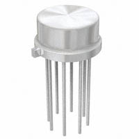
BOTTOM VIEW 8 7 Q2 6 Q1 7V 5 4 H8 PACKAGE TO-5 METAL CAN θJA = 80°C/W, θJA = 400°C/W 3 2 1
Heater to Substrate ...................................................35V Collector Emitter Breakdown Q1 ...............................15V Collector Emitter Breakdown Q2 ...............................35V Emitter Base Reverse Bias ..........................................2V Operating Temperature Range .........–55°C ≤ TA ≤ 125°C Storage Temperature Range.............–65°C ≤ TA ≤ 150°C Substrate Forward Bias ............................................0.1V
ORDER PART NUMBER LTZ1000ACH LTZ1000CH
PART MARKING
Order Options Lead Free: Add #PBF Lead Free Part Marking: http://www.linear.com/leadfree/ Consult LTC Marketing for parts specified with wider operating temperature ranges.
ELECTRICAL CHARACTERISTICS
PARAMETER Zener Voltage Zener Change with Current Zener Leakage Current Zener Noise Heater Resistance Heater Breakdown Voltage Transistor Q1 Breakdown Transistor Q2 Breakdown Q1, Q2 Current Gain Thermal Resistance Long Term Stability CONDITIONS
(Note 2)
MIN 7.0 6.9 TYP 7.2 7.15 80 20 1.2 200 35 15 35 80 Time = 5 Minutes Time = 5 Minutes 300 20 50 200 80 400 2 450 °C/W °C/W µV√kHr MAX 7.5 7.45 240 200 2 420 V V V UNITS V V mV µA µVP-P
lZ = 5mA, (VZ + VBEQ1) IQ1 = l00µA lZ = 1mA, (VZ + VBEQ1) IQ1 = l00A 1mA ≤ IZ < 5mA VZ = 5V lZ = 5mA, 0.1Hz < f < 10Hz 1Q1 = 100µA IL ≤ 100µA IC = 10µA, LVCEO IC = 10µA, LVCEO IC = 100µA LTZ1000 LTZ1000A T = 65°C
Note 1: Stresses beyond those listed under Absolute Maximum Ratings may cause permanent damage to the device. Exposure to any Absolute Maximum Rating condition for extended periods may affect device reliability and lifetime.
Note 2: All testing is done at 25°C. Pulse testing is used for LTZ1000A to minimize temperature rise during testing. LTZ1000 and LTZ1000A devices are QA tested at –55°C and 125°C.
1000afb
2
�LTZ1000/LTZ1000A PIN FUNCTIONS
Pin 1: Heater positive. Must have a higher positive value than Pin 2 and Pin 4. Pin 2: Heater negative. Must have a higher positive value than Pin 4. Must have equal or lower potential than Pin 1. Pin 3: Zener positive. Must have a higher positive value than Pin 4. Pin 4: Substrate and Zener negative. Must have a higher positive value than Pin 7. If Q1 is Zenered (about 7V) a permanent degradation in beta will result. Pin 5: Temperature compensating transistor collector. Pin 6: Temperature sensing transistor base. If the base emitter junction is Zenered (about 7V) the transistor will suffer permanent beta degradation. Pin 7: Emitter of sensing and compensating transistors. Pin 8: Collector of sensing transistor.
TYPICAL PERFORMANCE CHARACTERISTICS
Zener Voltage vs Current
100 90 ZENER VOLTAGE NOISE (nV/√Hz) ZENER VOLTAGE CHANGE (mV) 80 70 60 50 40 30 20 10 0 0 ZENER WITH KELVIN SENSED Q1 0.5 1.0 1.5 2.0 2.5 3.0 3.5 4.0 4.5 5.0 ZENER CURRENT (mA)
1000 G01
Zener Voltage Noise Spectrum
500 450 400 350 300 250 ZENER CURRENT = 0.5mA 200 150 100 50 0 0.1 ZENER CURRENT = 4mA
Zener Noise
IZ = 4mA
ZENER ALONE
ZENER VOLTAGE NOISE (2µV/D)
IZ = 0.5mA
1 10 FREQUENCY (Hz)
100
0
10
20 30 40 TIME (SECONDS)
50
60
1000 G02
1000 G03
Die Temperature Rise vs Heater Power
0.8 0.7 HEATER POWER (W) 0.6 0.5 0.4 0.3 0.2 0.1 0 25 35 45 55 65 75 85 95 105 115 125 DIE TEMPERATURE ABOVE AMBIENT (°C)
1000 G04
Die Temperature vs Time
125 LTZ1000A DIE TEMPERATURE RISE (°C) HEATER POWER = 0.3W 125
Die Temperature Rise vs Time
LTZ1000 100
LTZ1000
DIE TEMPERATURE RISE (°C)
100
75 HEATER POWER = 0.2W
75
HEATER POWER = 0.7W HEATER POWER = 0.5W
50
50
LTZ1000A
25
HEATER POWER = 0.1W
25 HEATER POWER = 0.3W
0 0.1
1
10 100 TIME (SECONDS)
1000
0 0.1
1
10 100 TIME (SECONDS)
1000 G06
1000
1000 G05
1000afb
3
�LTZ1000/LTZ1000A APPLICATIONS INFORMATION
LTZ1000 and LTZ1000A are capable of providing ultimate voltage reference performance. Temperature drifts of better than 0.03ppm/°C and long term stability on the order of 1µV per month can be achieved. Noise of about 0.15ppm can also be obtained. This performance is at the expense of circuit complexity, since external influences can easily cause output voltage shifts of more than 1ppm. Thermocouple effects are one of the worst problems and can give apparent drifts of many ppm/°C as well as cause low frequency noise. The kovar input leads of the TO-5 package form thermocouples when connected to copper PC boards. These thermocouples generate outputs of 35µV/°C. It is mandatory to keep the zener and transistor leads at the same temperature, otherwise 1ppm to 5ppm shifts in the output voltage can easily be expected from these thermocouples. Air currents blowing across the leads can also cause small temperature variations, especially since the package is heated. This will look like 1ppm to 5ppm of low frequency noise occurring over a several minute period. For best results, the device should be located in an enclosed area and well shielded from air currents. Certainly, any temperature gradient externally generated, say from a power supply, should not appear across the critical circuitry. The leads to the transistor and zener should be connected to equal size PC traces to equalize the heat loss and maintain them at similar temperatures. The bottom portion of the PC board should be shielded against air currents as well. Resistors, as well as having resistance temperature coefficients, can generate thermocouple effects. Some types of resistors can generate hundreds of microvolts of thermocouple voltage. These thermocouple effects in the resistor can also interfere with the output voltage. Wire wound resistors usually have the lowest thermocouple voltage, while tin oxide type resistors have very high thermocouple voltage. Film resistors, especially Vishay precision film resistors, can have low thermocouple voltage. Ordinary breadboarding techniques are not good enough to give stable output voltage with the LTZ1000 family devices. For breadboarding, it is suggested that a small printed circuit board be made up using the reference, the amplifier and wire wound resistors. Care must be taken to ensure that heater current does not flow through the same ground lead as the negative side of the reference (emitter of Q1). Current changes in the heater could add to, or subtract from, the reference voltage causing errors with temperature. Single point grounding using low resistance wiring is suggested. Setting Control Temperature The emitter-base voltage of the control transistor sets the stabilization temperature for the LTZ1000. With the values given in the applications, temperature is normally 60°C. This provides 15°C of margin above a maximum ambient of 45°C, for example. Production variations in emitter-base voltage will typically cause about ±10°C variation. Since the emitter-base voltage changes about 2mV/°C and is very predictable, other temperatures are easily set. Because higher temperatures accelerate aging and decrease long term stability, the lowest temperature consistent with the operating environment should be used. The LTZ1000A should be set about 10°C higher than the LTZ1000. This is because normal operating power dissipation in the LTZ1000A causes a temperature rise of about 10°C. Of course both types of devices should be insulated from ambient. Several minutes of warm-up is usual. For applications not requiring the extreme precision or the low noise of the LTZ1000, Linear Technology makes a broad line of voltage references. Devices like the LT1021 can provide drifts as low as 2ppm/°C and devices such as the LM399A can provide drifts of 1ppm/°C. Only applications requiring the very low noise or low drift with time of the LTZ1000 should use this device. See Application Notes AN-82 and AN-86 for further information. Consult the Linear Technology Applications department for additional help.
1000afb
4
�LTZ1000/LTZ1000A TYPICAL APPLICATIONS
Negative Voltage Reference
ZENER + SENSE V+ 15V GND 0.1µF 1 1k 2N3904 7 LT1013 R4 13k 8 3 6 10k 1M 2 0.1µF 400k* R5 1k 4 7 8 1 LT1013 3 R1 120 4 1N4148 0.022µF ZENER – FORCE ZENER – SENSE *PROVIDE TEMPERATURE COMPENSATION, DELETE FOR LTZ1000A APPROXIMATE CHANGE IN REFERENCE VOLTAGE FOR A 100ppm CHANGE IN RESISTOR VALUES: R1 R2 R3 R4/R5 RATIO 100ppm = ∆R(Ω) 0.012Ω 7Ω 7Ω ∆R = 0.01% ∆VZ 1ppm 0.3ppm 0.2ppm 1ppm
1000 TA02
R3 70k 5
R2 70k
+ –
5
2
– +
V – ≥ 10V
BOTH A1 AND A2 CONTRIBUTE LESS THAN 2µV OF OUTPUT DRIFT OVER A 50°C RANGE
Averaging Reference Voltage for Lower Noise and Better Stability
VIN 15V 0.01% 1.6k 1.6k VIN 15V 1.5k
Improving Supply Rejection
SUPPLY REJECTION AT VOUT1 = 20mV/V
VOUT1 50Ω VOUT2
30Ω*
30Ω*
SUPPLY REJECTION AT VOUT2 = 3mV/V
150Ω OUTPUT 150Ω 150Ω
1000 TA03
IC
1000 TA04
*R = kT q IC
1000afb
5
�LTZ1000/LTZ1000A TYPICAL APPLICATIONS
Adjusting Temperature Coefficient in Unstabilized Applications
15V VOUT + R1 200Ω* 3 5 2 4 120Ω 7 0.022µF 2 1N4148 70k 3 1N4148 1 1 MIN * ON OFF 1 MIN
+
LT1006 6
–
HEATER
4
* PULSE HEATER ON AND OFF TO HEAT AND COOL THE REFERENCE. ADJUST R1 FOR MINIMUM VOLTAGE CHANGE THROUGH A TEMPERATURE CYCLE. THE –2mV/°C TEMPCO OF THE VBE CANCELS THE +2mV/°C TEMPCO OF THE ZENER.
1000 TA05
7V Positive Reference Circuit
ZENER + SENSE V+ 15V R4 13k R3 3 70k 8 6 10k R2 70k 5 2 7 1M 0.1µF 1 400k* 0.1µF R5 1k R1 120 0.002µF 4 ZENER – SENSE
2N3904
1k
+
7 A1 LT1013
5
3
+ –
8 1
1N4148
A2 LT1013 4
–
GROUND ZENER – FORCE
2
1N4148
HEATER RETURN (TIED TO GROUND)
*PROVIDES TC COMPENSATION, DELETE FOR LTZ1000A APPROXIMATE CHANGE IN REFERENCE VOLTAGE FOR A 100ppm (0.01%) CHANGE IN RESISTOR VALUES: R1 R2 R3 R4/R5 RATIO ∆R(Ω) 0.012Ω 7Ω 7Ω ∆R = 0.01% ∆VZ 1ppm 0.3ppm 0.2ppm 1ppm
1000 TA06
BOTH A1 AND A2 CONTRIBUTE LESS THAN 2µV OF OUTPUT DRIFT OVER A 50°C RANGE
1000afb
6
�LTZ1000/LTZ1000A BLOCK DIAGRAM
1
8
3
5
*
*
Q2
Q1
2
6
4
7
1000 TA07
*SUBSTRATE DEVICES–DO NOT FORWARD BIAS
1000afb
Information furnished by Linear Technology Corporation is believed to be accurate and reliable. However, no responsibility is assumed for its use. Linear Technology Corporation makes no representation that the interconnection of its circuits as described herein will not infringe on existing patent rights.
7
�LTZ1000/LTZ1000A PACKAGE DESCRIPTION
H Package 8-Lead TO-5 Metal Can (.200 Inch PCD) (Reference LTC DWG # 05-08-1320)
.335 – .370 (8.509 – 9.398) DIA .305 – .335 (7.747 – 8.509) .040 (1.016) MAX .050 (1.270) MAX GAUGE PLANE .165 – .185 (4.191 – 4.699) REFERENCE PLANE .500 – .750 (12.700 – 19.050)
SEATING PLANE .010 – .045* (0.254 – 1.143) .016 – .021** (0.406 – 0.533)
45° .028 – .034 (0.711 – 0.864)
.027 – .045 (0.686 – 1.143) PIN 1
.200 (5.080) TYP
.110 – .160 (2.794 – 4.064) INSULATING STANDOFF *LEAD DIAMETER IS UNCONTROLLED BETWEEN THE REFERENCE PLANE AND THE SEATING PLANE .016 – .024 **FOR SOLDER DIP LEAD FINISH, LEAD DIAMETER IS (0.406 – 0.610) H8(TO-5) 0.200 PCD 0204
RELATED PARTS
PART NUMBER LM399 LT1021 LT1236 LT1389 LT1634 DESCRIPTION 7V Precision Shunt Reference 5V, 7V and 10V Precision Reference 5V and 10V Low Drift Precision Reference 1.25V, 2.5V, 4V and 5V Nanopower Shunt Reference 1.25V and 2.5V Micropower Shunt Reference COMMENTS 0.2% Accuracy, 0.5ppm/°C Drift, 20µVRMS Noise Available in T0-5, –55°C to 125°C, Series or Shunt Operation 0.05% Accuracy, 5ppm/°C Drift, Series or Shunt Operation 800nA, 0.05% Accuracy, 10ppm/°C Drift 0.05%, 10ppm/°C, 10µA Current
1000afb
8
Linear Technology Corporation
1630 McCarthy Blvd., Milpitas, CA 95035-7417
(408) 432-1900 ● FAX: (408) 434-0507
●
LT 0206 REV B • PRINTED IN USA
www.linear.com
© LINEAR TECHNOLOGY CORPORATION 1987
�