Optical Sensor
Product Data Sheet
LTR-303ALS-01
Spec No.: DS86-2013-0004
Effective Date: 07/09/2014
Revision: A
LITE-ON DCC
RELEASE
BNS-OD-FC001/A4
LITE-ON Technology Corp. / Optoelectronics
No.90,Chien 1 Road, Chung Ho, New Taipei City 23585, Taiwan, R.O.C.
Tel: 886-2-2222-6181 Fax: 886-2-2221-1948 / 886-2-2221-0660
http://www.liteon.com/opto
�Optical Sensor
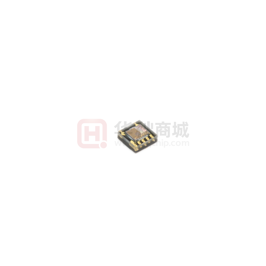
LTR-303ALS-01
1. Description
2
The LTR-303ALS-01 is a low voltage I C digital light sensor [ALS] in a low cost miniature chipled lead-free surface mount
2
package. This sensor converts light intensity to a digital output signal capable of direct I C interface. It provides a linear
response over a wide dynamic range from 0.01 lux to 64k lux and is well suited to applications under high ambient
brightness. There are altogether six gain settings (1X, 2X, 4X, 8X, 48X and 96X) available for user to configure.
The sensor supports an interrupt feature that removes the need to poll the sensor for a reading which improves system
efficiency. The sensor also supports several features that help to minimize the occurrence of false triggering. This CMOS
design and factory-set one time trimming capability ensure minimal sensor-to-sensor variations for ease of manufacturability
to the end customers.
2. Features
I C interface (Fast Mode @ 400kbit/s)
Ultra-small 6-pin ChipLED package
2.0mm(L), 2.0mm(B), 0.7mm(H)
Built-in temperature compensation circuit
Low active power consumption with standby mode
Supply voltage range from 2.4V to 3.6V capable of 1.7V logic voltage
Operating temperature range from -
RoHS and Halogen free compliant
Close to human eye spectral response
Immunity to IR / UV Light Source
Automatically rejects 50 / 60 Hz lightings flicker
Full dynamic range from 0.01 lux to 64k lux
16-bit effective resolution
2
1/31
Part No. : LTR-303ALS-01
BNS-OD-FC002/A4
�Optical Sensor
LTR-303ALS-01
3. Applications
Back-lighting Control in mobile/portable devices
Touch Panel Control in mobile/portable devices
4. Ordering Information
Part Number
Packaging Type
Package
Quantity
LTR-303ALS-01
Tape and Reel
6-pin chipled package
2500
5. Outline Dimensions
2/31
Part No. : LTR-303ALS-01
BNS-OD-FC002/A4
�Optical Sensor
LTR-303ALS-01
6. Functional Block Diagram
7. Application Circuit
3/31
Part No. : LTR-303ALS-01
BNS-OD-FC002/A4
�Optical Sensor
LTR-303ALS-01
I/O Pins Configuration Table
Pin
I/O Type
Symbol
Description
1
VDD
Power Supply Voltage
2
NC
No connection to this pin
3
GND
Ground
2
4
I
SCL*
I C serial clock. This pin is an open drain input.
5
O
INT*
Level Interrupt Pin. This pin is an open drain output.
6
I/O
SDA*
I C serial data. This pin is an open drain input / output.
2
* Note: For noisy environment, add 10pF capacitor from signal to GND for additional noise filtering.
Recommended Application Circuit Components
[1]
Component
Recommended Value
Rp1, Rp2, Rp3 [1]
1 k to 10 k
C1
1uF 20%, X7R / X5R Ceramic
Selection of pull-up resistors value is dependent on bus capacitance values. For more details, please refer to I 2C Specifications:
http://www.nxp.com/documents/user_manual/UM10204.pdf
4/31
Part No. : LTR-303ALS-01
BNS-OD-FC002/A4
�Optical Sensor
LTR-303ALS-01
8. Ratings and Specifications
Absolute Maximum Ratings at Ta = 25C
Parameter
Symbol
Rating
Unit
3.8
V
Supply Voltage
VDD
Digital Voltage Range
SCL, SDA, INT
-0.5 to 3.8
V
Digital Output Current
SCL, SDA, INT
-1 to 20
mA
Storage Temperature
Tstg
-40 to 100
C
Note: Exceeding these ratings could cause damage to the sensor. All voltages are with respect to ground. Currents are
positive into, negative out of the specified terminal.
Recommended Operating Conditions
Description
Symbol
Supply Voltage
VDD
Interface Bus Power Supply Voltage
VIO
Min.
VIH SCL,
I2C Bus Input Pin High Voltage
Typ.
Max.
Unit
2.4
3.6
V
1.7
3.6
V
1.2
V
VIH SDA
VIL SCL,
I2C Bus Input Pin Low Voltage
0.6
V
70
C
VIL SDA
Operating Temperature
Tope
-30
Electrical & Optical Specifications
All specifications are at VDD = 3.0V, Tope = 25C, unless otherwise noted.
Parameter
Min.
Active Supply Current
Standby Current
Initial Startup Time
Wakeup Time from Standby
Typ.
Max.
Unit
Condition
220
uA
Active Mode,
Tope = 25C, VDD=3.6V
Integration Time : 100ms
Measurement rate : 200ms
5
uA
Standby / Sleep Mode
ms
(Note 1)
ms
(Note 1)
100
10
5/31
Part No. : LTR-303ALS-01
BNS-OD-FC002/A4
�Optical Sensor
LTR-303ALS-01
Light Sensor
Parameter
Min.
Max.
Unit
65535
count
0
6
count
Ch0, Lux = 0
0
6
count
Ch1, Lux = 0
Full Scale ADC Count
Typ.
Condition
Dark ADC Count
Ch0
(see note 2)
3250
6100
count
white LED 200 Lux
Integration Time : 50ms
Measurement Time : 100ms
ADC Count (Gain=96)
Ch1
@200Lux
(see note 2)
1050
1950
count
White LED 200 Lux
Integration Time : 50ms
Measurement Time : 100ms
0.15
0.35
Ratio
Ch1/(Ch0 + Ch1)
Notes:
1.
Startup Sequence
Supply VDD to Sensor
(Sensor in Standby Mode)
Wait at least 100 ms - initial startup time
I2C Command (Write)
To enable sensor to Active Mode
Wait at least 10 ms - wakeup time from standby
Sensor is Active and starts measurement
2.
LiteOn White LED color temperature 10000K.
6/31
Part No. : LTR-303ALS-01
BNS-OD-FC002/A4
�Optical Sensor
LTR-303ALS-01
Typical Performance Curve
All specifications are at VDD = 3.0V, Tope = 25C, unless otherwise noted.
Figure 1: Normalized Spectral Response
Figure 2 : Viewing angle
7/31
Part No. : LTR-303ALS-01
BNS-OD-FC002/A4
�Optical Sensor
LTR-303ALS-01
Figure 3 : Vdd versus Average Idd
Figure 4 : Average Idd versus temperature
8/31
Part No. : LTR-303ALS-01
BNS-OD-FC002/A4
�Optical Sensor
LTR-303ALS-01
Figure 5 : Output count ratio versus temperature
Lux Formula
Refer to Appendix A for the lux formula
9/31
Part No. : LTR-303ALS-01
BNS-OD-FC002/A4
�Optical Sensor
LTR-303ALS-01
AC Electrical Characteristics
All specifications are at VBus = 1.8V, Tope = 25C, unless otherwise noted.
Parameter
Symbol
Min.
Max.
Unit
SCL clock frequency
1
Bus free time between a STOP and START condition
f SCL
t BUF
400
kHz
1.3
us
Hold time (repeated) START condition. After this period, the first
clock pulse is generated
t H D; S TA
0.6
us
LOW period of the SCL clock
1.3
us
HIGH period of the SCL clock
t LOW
t HIGH
0.6
us
Set-up time for a repeated START condition
t S U ; S TA
0.6
us
Set-up time for STOP condition
t S U ; S TO
0.6
us
Rise time of both SDA and SCL signals
tr
30
300
ns
Fall time of both SDA and SCL signals
tf
30
300
ns
Data hold time
t H D; D AT
0.3
0.9
us
Data setup time
t S U ; D AT
100
Pulse width of spikes which must be suppressed by the input filter
t SP
0
ns
50
ns
2
Definition of timing for I C bus
10/31
Part No. : LTR-303ALS-01
BNS-OD-FC002/A4
�Optical Sensor
LTR-303ALS-01
9. Principles of Operation
2
I C Protocols
.I2C Write Protocol (type 1):
1
7
1
1
8
1
1
S Slave address W
A
Register Address
A P
1
8
Slave ID (Write)
Slave ID (Write)
1
2
3
4
5
6
7
8
S
6
S
5
S
4
S
3
S
2
S
1
S
0
9
2
3
4
5
6
7
9
SCL
SDA
S
Slave address
A A A A A A A A
7 6 5 4 3 2 1 0
W A
Register Address
A
P
2
.I C Write Protocol (type 2):
1
7
1
1
8
1
S Slave address W
A
Register Address
8
1
1
A Register Command A P
Slave ID (Write)
Slave ID (Write)
1
2
3
4
5
6
7
8
S
6
S
5
S
4
S
3
S
2
S
1
S
0
9
1
2
3
4
5
6
7
8
9
1
2
3
4
5
6
7
8
9
SCL
SDA
S
A A A A A A A A
7 6 5 4 3 2 1 0
Slave address
W A
Register Address
A A A A A A A A
7 6 5 4 3 2 1 0
A
Register Command
A
P
2
.I C Read Protocol:
1
7
1
1
S Slave address R
8
1
1
A Register Command N P
Slave ID (Read)
Slave ID (Read)
1
2
3
4
5
6
7
S
6
S
5
S
4
S
3
S
2
S
1
S
0
8
9
1
2
3
4
5
6
7
8
9
SCL
SDA
S
Slave address
C C C C C C C C
7 6 5 4 3 2 1 0
R A
Register Command
N
P
11/31
Part No. : LTR-303ALS-01
BNS-OD-FC002/A4
�Optical Sensor
LTR-303ALS-01
2
.I C Read (Combined format) Protocol:
1
1
8
S Slave address W
1
7
A
Register Address
1
1
7
A Sr Slave address
Slave ID (Write)
1
1
R
A Register Command N P
2
3
4
1
1
Slave ID (Read)
Slave ID (Write)
1
8
5
6
Slave ID (Read)
7
8
9
1
2
3
4
5
6
7
8
9
1
2
3
4
5
6
7
8
9
……
SCL
S
6
SDA
S
S
5
S
4
S
3
S
2
S
1
S
0
Slave address
A A A A A A A A
7 6 5 4 3 2 1 0
W A
Register Address
A
S
6
S
5
1
2
Sr
S
4
S
3
S
2
S
1
S
0
6
7
Slave address
3
4
5
……
R A
8
9
……
C C C C C C C C
7 6 5 4 3 2 1 0
……
A
Register Command
N
A
Acknowledge (0 for an ACK)
N
Non-Acknowledge(1 for an NACK)
S
Start condition
Sr
Repeated Start condition
P
Stop condition
W
Write (0 for writing)
R
Read (1 for read)
Slave-to-master
P
Master-to-Slave
2
I C Slave Address
The 7 bits slave address for this sensor is 0x29H. A read/write bit should be appended to the slave address by the master device
to properly communicate with the sensor.
I2C Slave Address
(0x29H)
W/R
Command
Type
Bit7
Bit6
Bit5
Bit4
Bit3
Bit2
Bit1
Bit0
Write
0
1
0
1
0
0
1
0
0x52H
Read
0
1
0
1
0
0
1
1
0x53H
value
12/31
Part No. : LTR-303ALS-01
BNS-OD-FC002/A4
�Optical Sensor
LTR-303ALS-01
Register Set
Addr
R/W
Register Name
Description
Reset Value
0x80
R/W
ALS_CONTR
ALS operation mode control SW reset
0x00
0x85
R/W
ALS_MEAS_RATE
ALS measurement rate in active mode
0x01
0x86
R
PART_ID
Part Number ID and Revision ID
0xA0
0x87
R
MANUFAC_ID
Manufacturer ID
0x05
0x88
R
ALS_DATA_CH1_0
ALS measurement CH1 data, lower byte
0x00
0x89
R
ALS_DATA_CH1_1
ALS measurement CH1 data, upper byte
0x00
0x8A
R
ALS_DATA_CH0_0
ALS measurement CH0 data, lower byte
0x00
0x8B
R
ALS_DATA_CH0_1
ALS measurement CH0 data, upper byte
0x00
0x8C
R
ALS_STATUS
ALS new data status
0x00
0x8F
R/W
INTERRUPT
Interrupt settings
0x08
0x97
R/W
ALS_THRES_UP_0
ALS interrupt upper threshold, lower byte
0xFF
0x98
R/W
ALS_THRES_UP_1
ALS interrupt upper threshold, upper byte
0xFF
0x99
R/W
ALS_THRES_LOW_0
ALS interrupt lower threshold, lower byte
0x00
0x9A
R/W
ALS_THRES_LOW_1
ALS interrupt lower threshold, upper byte
0x00
0x9E
R/W
INTERRUPT PERSIST
ALS Interrupt persist setting
0x00
Notes:
1)
When reading ALS data registers, read sequence should always be from lower address to higher address (E.g. For ALS
data, Ch1 data should be read first followed by Ch0 data. Read sequence should be 0x88, 0x89, 0x8A, 0x8B. When 0x8B is
read, all four ALS data registers will be populated with new set of data).
2)
When setting of INTERRUPT register (addr 0x8F) is necessary, it should be done before the device is in Active mode.
13/31
Part No. : LTR-303ALS-01
BNS-OD-FC002/A4
�Optical Sensor
LTR-303ALS-01
ALS_CONTR Register (0x80)
The ALS_CONTR register controls the ALS Gain setting, ALS operation modes and software (SW) reset for the sensor.
2
The ALS sensor can be set to either standby mode or active mode. At either of these modes, the I C circuitry is always
active. The default mode after power up is standby mode. During standby mode, there is no ALS measurement performed
2
but I C communication is allowed to enable read/write to all the registers
0x80
ALS_CONTR (default = 0x00)
B7
B6
B5
B4
Reserved
Bits
Default
Type
Reserved
7:5
000
--
4:2
000
1
0
B1
B0
SW Reset
ALS Mode
Description
--
MUST write to 000 (default)
000
Gain 1X 1 lux to 64k lux (default)
001
Gain 2X 0.5 lux to 32k lux
010
Gain 4X 0.25 lux to 16k lux
011
Gain 8X 0.125 lux to 8k lux
100
Reserved
101
Reserved
110
Gain 48X 0.02 lux to 1.3k lux
111
Gain 96X 0.01 lux to 600 lux
RW
0
SW reset
B2
ALS Gain
Field
ALS Gain
B3
RW
Initial start-up procedure is NOT started (default)
Initial start-up procedure is started, bit has default
1
value of 0 after start-up
ALS mode
0
0
0
Stand-by mode (default)
1
Active mode
RW
14/31
Part No. : LTR-303ALS-01
BNS-OD-FC002/A4
�Optical Sensor
LTR-303ALS-01
ALS_MEAS_RATE Register (0x85)
The ALS_MEAS_RATE register controls the integration time and timing of the periodic measurement of the ALS in active
mode. ALS Measurement Repeat Rate is the interval between ALS_DATA registers update. ALS Integration Time is the
measurement time for each ALS cycle. ALS Integration Time must be set to be equal or smaller than the ALS
Measurement Repeat Rate. If ALS Integration Time is set to be bigger than ALS Measurement Repeat Rate, it will be
automatically reset to be equal to ALS Measurement Repeat Rate by the IC internally.
0x85
ALS_MEAS_RATE (default = 0x03)
B7
B6
B5
Reserved
Bits
Default
Type
Reserved
7:6
00
--
ALS
measurement
rate
5:3
2:0
B3
ALS Integration Time
Field
ALS
integration
time
B4
000
011
B2
B1
B0
ALS Measurement Repeat Rate
Description
--
--
000
100ms (default)
001
50ms
010
200ms
011
400ms
100
150ms
101
250ms
110
300ms
111
350ms
000
50ms
001
100ms
010
200ms
011
500ms (default)
100
1000ms
RW
RW
101
110
2000ms
111
15/31
Part No. : LTR-303ALS-01
BNS-OD-FC002/A4
�Optical Sensor
LTR-303ALS-01
PART_ID Register (0x86) (Read Only)
The PART_ID register defines the part number and revision identification of the sensor.
0x86
PART_ID (default = 0xA0)
B7
B6
B5
B4
B3
Part Number ID
B2
B1
B0
Revision ID
Field
Bits
Default
Type
Description
Part Number ID
7:4
1010
R
Part ID 0x0AH
Revision ID
3:0
0000
R
Revision ID 0x00H
MANUFAC_ID Register (0x87) (Read Only)
The MANUFAC_ID register defines the manufacturer identification of the sensor.
0x87
MANUFAC_ID (default = 0x05)
B7
B6
B5
B4
B3
B2
B1
B0
Manufacturer ID
Field
Bits
Default
Type
Manufacturer ID
7:0
00000101
R
Description
Manufacturer ID (0x05H)
16/31
Part No. : LTR-303ALS-01
BNS-OD-FC002/A4
�Optical Sensor
LTR-303ALS-01
ALS_DATA_CH1 Register (0x88 / 0x89) (Read Only)
The ALS_DATA registers should be read as a group, with the lower address read back first (i.e. read 0x88 first, then read
0x89). These two registers should also be read before reading channel-0 data (from registers 0x8A, 0x8B).
2
2
When the I C read operation starts, all four ALS data registers are locked until the I C read operation of register 0x8B is
completed. This will ensure that the data in the registers is from the same measurement even if an additional integration
cycle ends during the read operation. New measurement data is stored into temporary registers and the ALS_DATA
2
registers are updated as soon as there is no on-going I C read operation.
The ALS ADC channel-1 data is expressed as a 16-bit data spread over two registers. The ALS_DATA_CH1_0 and
ALS_DATA_CH1_1 registers provide the lower and upper byte respectively.
0x88
ALS_DATA_CH1_0 (default = 0x00)
B7
B6
B5
B4
B3
B2
B1
B0
B2
B1
B0
ALS Data Ch1 Low
0x89
ALS_DATA_CH1_1 (default = 0x00)
B7
B6
B5
B4
B3
ALS Data Ch1 High
Field
Address
Bits
Default
Type
Description
ALS Data Ch1 Low
0x88
7:0
00000000
R
ALS ADC channel 1 lower byte data
ALS Data Ch1 High
0x89
7:0
00000000
R
ALS ADC channel 1 upper byte data
17/31
Part No. : LTR-303ALS-01
BNS-OD-FC002/A4
�Optical Sensor
LTR-303ALS-01
ALS_DATA_CH0 Register (0x8A / 0x8B) (Read Only)
These two registers should be read after reading channel-1 data (from registers 0x88, 0x89). Lower address register
should be read first (i.e. read 0x8A first, then read 0x8B). See ALS_DATA_CH1 register information above. The ALS ADC
channel-0 data is expressed as a 16-bit data spread over two registers. The ALS_DATA_CH0_0 and ALS_DATA_CH0_1
registers provide the lower and upper byte respectively.
0x8A
ALS_DATA_CH0_0 (default = 0x00)
B7
B6
B5
B4
B3
B2
B1
B0
B2
B1
B0
ALS Data Ch0 Low
0x8B
ALS_DATA_CH0_1 (default = 0x00)
B7
B6
B5
B4
B3
ALS Data Ch0 High
Field
Address
Bits
Default
Type
Description
ALS Data Ch0 Low
0x8A
7:0
00000000
R
ALS ADC channel 0 lower byte data
ALS Data Ch0 High
0x8B
7:0
00000000
R
ALS ADC channel 0 upper byte data
18/31
Part No. : LTR-303ALS-01
BNS-OD-FC002/A4
�Optical Sensor
LTR-303ALS-01
ALS_ STATUS Register (0x8C) (Read Only)
The ALS_STATUS register stores the information about ALS data status.
New data means data has not been read yet.
When the measurement is completed and data is written to the data register, the data status bit will be set to logic 1. When
the data register is read, the data status bit will be set to logic 0.
Interrupt status determines if the ALS interrupt criteria are met. It will check if the ALS measurement data is outside of the
range defined by the upper and lower threshold limits.
0x8C
ALS_STATUS (default = 0x00)
B7
B6
ALS Data
Valid
B5
ALS Gain
Field
Bits
Default
Type
ALS Data Valid
7
0
R
ALS Data Gain
Range
6:4
B4
000
3
ALS data
status
2
Reserved
1:0
0
B2
ALS
Interrupt
Status
ALS Data
Status
B1
B0
Reserved
Description
0
ALS Data is Valid (default)
1
ALS Data is Invalid
000
ALS measured data in Gain 1X (default)
001
ALS measured data in Gain 2X
010
ALS measured data in Gain 4X
011
ALS measured data in Gain 8X
100
Invalid
101
Invalid
110
ALS measured data in Gain 48X
111
ALS measured data in Gain 96X
R
0
ALS interrupt
status
B3
Interrupt signal INACTIVE (default)
R
Interrupt signal ACTIVE
0
00
0
OLD data (data already read), (default)
1
NEW data (first time data is being read)
--
Don’t care
R
R
19/31
Part No. : LTR-303ALS-01
BNS-OD-FC002/A4
�Optical Sensor
LTR-303ALS-01
INTERRUPT Register (0x8F) (Read Only)
The INTERRUPT register controls the operation of the interrupt pin and functions. When the Interrupt Mode is set to 00,
the INT output pin 2 is inactive / disabled and will not trigger any interrupt.
Note that when this register is to be set with values other than its default values, it should be set before device is in Active
mode.
0x8F
INTERRUPT (default = 0x08)
B7
B6
B5
B4
B3
Reserved
Field
Bits
Default
Type
RESERVED
7:3
00001
--
Interrupt
Polarity
2
0
RW
Interrupt Mode
1
RESERVED
0
0
--
B0
Interrupt
Polarity
Interrupt
Mode
Reserved
Must write as 00000
Bit B3 is “1” (default) but it has no impact on
performance
INT pin is considered active when it is a logic 0
(default)
1
INT pin is considered active when it is a logic 1
0
Interrupt pin is INACTIVE / high impedance state
(default)
1
ALS measurement can trigger interrupt
--
Don’t care
RW
--
B1
Description
0
0
B2
20/31
Part No. : LTR-303ALS-01
BNS-OD-FC002/A4
�Optical Sensor
LTR-303ALS-01
ALS_THRES Register (0x97 / 0x98 / 0x99 / 0x9A)
The ALS_THRES_UP and ALS_THRES_LOW registers determines the upper and lower limit of the interrupt threshold
value respectively. These two values form a range and the interrupt function compares if the measurement value in
ALS_DATA registers is inside or outside the range. The interrupt function is active if the measurement data is outside the
range defined by the upper and lower limits. The data format for ALS_THRES must be the same as ALS_DATA registers.
0x97
ALS_THRES_UP_0 (default = 0xFF)
B7
B6
B5
B4
B3
B2
B1
B0
B1
B0
B1
B0
B1
B0
ALS Upper Threshold Low
0x98
ALS_THRES_UP_1 (default = 0xFF)
B7
B6
B5
B4
B3
B2
ALS Upper Threshold High
0x99
ALS_THRES_LOW_0 (default = 0x00)
B7
B6
B5
B4
B3
B2
ALS Lower Threshold Low
0x9A
ALS_THRES_LOW_1 (default = 0x00)
B7
B6
B5
B4
B3
B2
ALS Lower Threshold High
Field
Address
Bits
Default
Type
Description
ALS upper threshold
Low
0x97
7:0
11111111
RW
ALS upper threshold lower byte data
ALS upper threshold
High
0x98
7:0
11111111
RW
ALS upper threshold upper byte data
ALS lower threshold
Low
0x99
7:0
00000000
RW
ALS lower threshold lower byte data
ALS lower threshold
High
0x9A
7:0
00000000
RW
ALS lower threshold upper byte data
21/31
Part No. : LTR-303ALS-01
BNS-OD-FC002/A4
�Optical Sensor
LTR-303ALS-01
INTERRUPT PERSIST Register (0x9E)
The INTERRUPT PERSIST register controls the N number of times the measurement data is outside the range
defined by the upper and lower threshold limits before asserting the INT output pin 2.
0x9E
INTERRUPT PERSIST (default = 0x00)
B7
B6
B5
B4
B3
RESERVED
Field
Bits
Default
Type
RESERVED
7:4
0000
--
ALS Persist
3:0
0000
B2
B1
B0
ALS Persist
Description
Don’t care
0000
Every ALS value out of threshold range (default)
0001
2 consecutive ALS values out of threshold range
RW
--1111
--16 consecutive ALS values out of threshold range
22/31
Part No. : LTR-303ALS-01
BNS-OD-FC002/A4
�Optical Sensor
LTR-303ALS-01
10. Device Operation(using Interrupt)
Below flow diagram illustrates the LTR-303ALS operation.
23/31
Part No. : LTR-303ALS-01
BNS-OD-FC002/A4
�Optical Sensor
LTR-303ALS-01
11. Device Operation(without using Interrupt)
Below flow diagram illustrates the LTR-303ALS operation without the use of interrupts.
24/31
Part No. : LTR-303ALS-01
BNS-OD-FC002/A4
�Optical Sensor
LTR-303ALS-01
12. Pseudo Codes Examples
Control Registers
// The Control Register defines the operating modes and gain settings of the ALS of LTR-303.
// Default settings is 0x00 (in Standby mode).
Slave_Addr = 0x29
// Enable ALS
Register_Addr = 0x80
Command = 0x01
// Slave address of LTR-303 device
// ALS_CONTR register
// For Gain X1
// For Gain X96, Command = 0x1D
WriteByte(Slave_Addr, Register_Addr, Command)
ALS Measurement Rate
// The ALS_MEAS_RATE register controls the ALS integration time and measurement rate.
// Default setting of the register is 0x03 (integration time 100ms, repeat rate 500ms)
Slave_Addr = 0x29
// Slave address of LTR-303 device
// Set ALS Integration Time 200ms, Repeat Rate 200ms
Register_Addr = 0x85
// ALS_MEAS_RATE register
Command = 0x12
// Int time = 200ms, Meas rate = 200ms
// For Int time = 400ms, Meas rate = 500ms, Command = 0x1B
WriteByte(Slave_Addr, Register_Addr, Command)
ALS Data Registers (Read Only)
// The ALS Data Registers contain the ADC output data for the respective channel.
// These registers should be read as a group, with the lower address being read first.
Slave_Addr = 0x29
// Read back ALS_DATA_CH1
Register_Addr = 0x88
ReadByte(Slave_Addr, Register_Addr, Data0)
Register_Addr = 0x89
ReadByte(Slave_Addr, Register_Addr, Data1)
// Read back ALS_DATA_CH0
Register_Addr = 0x8A
ReadByte(Slave_Addr, Register_Addr, Data2)
Register_Addr = 0x8B
ReadByte(Slave_Addr, Register_Addr, Data3)
ALS_CH1_ADC_Data = (Data1 8
// To convert decimal 1000 into two eight bytes register values
Data0 = 1000 & 0xFF
WriteByte(Slave_Addr, ALS_Upp_Threshold_Reg_0, Data0)
WriteByte(Slave_Addr, ALS_Upp_Threshold_Reg_1, Data1)
// Lower Threshold Setting (decimal 200)
ALS_Low_Threshold_Reg_0 = 0x99
// ALS Lower Threshold Low Byte Register address
ALS_Low_Threshold_Reg_1 = 0x9A
// ALS Lower Threshold High Byte Register address
Data1 = 200 >> 8
// To convert decimal 200 into two eight bytes register values
Data0 = 200 & 0xFF
WriteByte(Slave_Addr, ALS_Low_Threshold_Reg_0, Data0)
WriteByte(Slave_Addr, ALS_Low_Threshold_Reg_1, Data1)
WriteByte(Slave_Addr, ALS_Upp_Threshold_Reg_1, Data1)
26/31
Part No. : LTR-303ALS-01
BNS-OD-FC002/A4
�Optical Sensor
LTR-303ALS-01
13. Recommended Leadfree Reflow Profile
MAX 260C
T - TEMPERATURE (°C)
255
R3
230
217
200
180
R2
R4
60 sec to 90 sec
Above 217 C
150
R5
R1
120
80
25
0
P1
HEAT
UP
100
50
150
P2
SOLDER PASTE DRY
200
P3
SOLDER
REFLOW
250
P4
COOL DOWN
300
t-TIME
(SECONDS)
Process Zone
Symbol
T
Maximum T/time or Duration
Heat Up
P1, R1
25C to 150C
3C/s
Solder Paste Dry
P2, R2
150C to 200C
100s to 180s
P3, R3
200C to 260C
3C/s
P3, R4
260C to 200C
-6C/s
P4, R5
200C to 25C
-6C/s
Time maintained above liquidus point , 217C
> 217C
60s to 90s
Peak Temperature
260C
-
Time within 5C of actual Peak Temperature
> 255C
20s
Time 25C to Peak Temperature
25C to 260C
8mins
Solder Reflow
Cool Down
It is recommended to perform reflow soldering no more than twice.
27/31
Part No. : LTR-303ALS-01
BNS-OD-FC002/A4
�Optical Sensor
LTR-303ALS-01
14. Moisture Proof Packaging
All LTR-303ALS-01 are shipped in moisture proof package. Once opened, moisture absorption begins. This part is
compliant to JEDEC J-STD-033A Level 3.
Time from Unsealing to Soldering
After removal from the moisture barrier bag, the parts should be stored at the recommended storage conditions and
soldered within seven days. When the moisture barrier bag is opened and the parts are exposed to the recommended
storage conditions for more than seven days, the parts must be baked before reflow to prevent damage to the parts.
Recommended Storage Conditions
Storage Temperature
10C to 30C
Relative Humidity
Below 60% RH
Baking Conditions
Package
Temperature
Time
In Reels
60C
48 hours
In Bulk
100C
4 hours
Baking should only be done once.
28/31
Part No. : LTR-303ALS-01
BNS-OD-FC002/A4
�Optical Sensor
LTR-303ALS-01
15. Recommended Land Pattern and Metal Stencil Aperture
Recommended Land Pattern
Note: All dimensions are in millimeters
29/31
Part No. : LTR-303ALS-01
BNS-OD-FC002/A4
�Optical Sensor
LTR-303ALS-01
Recommended Metal Stencil Aperture
It is recommended that the metal stencil used for solder paste printing has a thickness (t) of 0.11mm (0.004 inches / 4 mils)
or 0.127mm (0.005 inches / 5 mils).
The stencil aperture opening is recommended to be 0.72mm x 0.60mm which has the same dimension as the land
pattern. This is to ensure adequate printed solder paste volume and yet no shorting.
Note:
1. All dimensions are in millimeters
30/31
Part No. : LTR-303ALS-01
BNS-OD-FC002/A4
�Optical Sensor
LTR-303ALS-01
16. Package Dimension for Tape and Reel
Notes:
1. All dimensions are in millimeters (inches)
2. Empty component pockets sealed with top cover tape
3. 7 inch reel - 2500 pieces per reel
4. In accordance with ANSI/EIA 481-1-A-1994 specifications.
31/31
Part No. : LTR-303ALS-01
BNS-OD-FC002/A4
�