L IT E - O N T E CH NO L O G Y CO RP O RAT IO N
Property of LITE-ON Only
FEATURES
* High current transfer ratio ( CTR : MIN. 1000% at IF = 1mA, VCE = 2V ) * High input-output isolation voltage ( Viso = 3,750Vrms ) * High collector-emitter voltage ( VCEO = 300V ) * Mini-flat package : 2.0mm profile : LTV-352T-TP * UL approved * CSA approved * FIMKO approved * NEMKO approved * DEMKO approved * SEMKO approved * VDE approved (*Requires “V” ordering option) * RoHS compliance
May.2009
APPLICATIONS
* Hybrid substrates that require high density mounting. * Telephone sets * Copiers, facsimiles * Interfaces with various power supply circuits, power distribution boards.
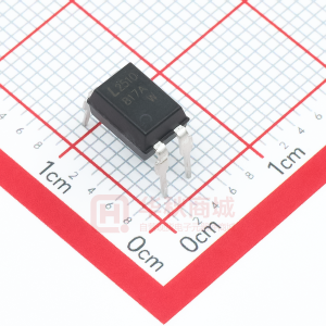
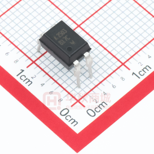
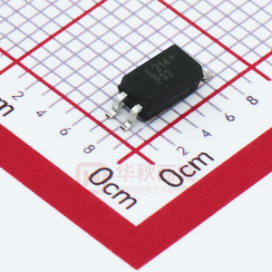
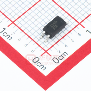
Part No. : LTV-352T-TP
BNS-OD-C131/A4
Page : 1
of 10
�L IT E - O N T E CH NO L O G Y CO RP O RAT IO N
Property of LITE-ON Only
OUTLINE DIMENSIONS
LTV-352T-TP :
*1. *2. *3. *4.
2-digit date code. Factory identification mark shall be marked (Z : Taiwan, Y : Thailand, X : China). Rank shall be or shall not be marked. VDE 0884 Identification.
Part No. : LTV-352T-TP
BNS-OD-C131/A4
Page : 2
of 10
�L IT E - O N T E CH NO L O G Y CO RP O RAT IO N
Property of LITE-ON Only
TAPING DIMENSIONS
Description Tape wide Pitch of sprocket holes Distance of compartment Distance of compartment to compartment
Symbol W P0 F P2 P1
Dimensions in mm ( inches ) 12 ± 0.3 ( .47 ) 4 ± 0.1 ( .15 ) 5.5 ± 0.1 ( .217 ) 2 ± 0.1 ( .079 ) 8 ± 0.1 ( .315 )
Part No. : LTV-352T-TP
BNS-OD-C131/A4
Page : 3
of 10
�L IT E - O N T E CH NO L O G Y CO RP O RAT IO N
Property of LITE-ON Only
ABSOLUTE MAXIMUM RATING
( Ta = 25°C )
PARAMETER Forward Current INPUT Reverse Voltage Power Dissipation Collector - Emitter Voltage Emitter - Collector Voltage OUTPUT Collector Current Collector Power Dissipation Total Power Dissipation *1 Isolation Voltage Operating Temperature Storage Temperature *2 Soldering Temperature IC PC Ptot Viso Topr Tstg Tsol 150 150 170 3,750 -55 ~ +110 -55 ~ +150 260 mA mW mW Vrms °C °C °C SYMBOL IF VR P VCEO VECO RATING 50 6 70 300 0.1 UNIT mA V mW V V
*1. AC For 1 Minute, R.H. = 40 ~ 60% Isolation voltage shall be measured using the following method. (1) Short between anode and cathode on the primary side and between collector and emitter on the secondary side. (2) The isolation voltage tester with zero-cross circuit shall be used. (3) The waveform of applied voltage shall be a sine wave. *2. For 10 Seconds
Part No. : LTV-352T-TP
BNS-OD-C131/A4
Page : 4
of 10
�L IT E - O N T E CH NO L O G Y CO RP O RAT IO N
Property of LITE-ON Only
ELECTRICAL - OPTICAL CHARACTERISTICS
( Ta = 25°C )
PARAMETER Forward Voltage INPUT Reverse Current Terminal Capacitance Collector Dark Current Collector-Emitter Breakdown Voltage Emitter-Collector Breakdown Voltage Collector Current *1 Current Transfer Ratio Collector-Emitter Saturation Voltage Isolation Resistance Floating Capacitance Cut-Off Frequency Response Time (Rise) Response Time (Fall) SYMBOL MIN. TYP. MAX. UNIT VF IR Ct ICEO BVCEO — — — — 300 1.2 — 30 — — 1.4 10 250 200 — V µA pF nA V CONDITIONS IF=10mA VR=4V V=0, f=1KHz VCE=200V, IF=0 IC=0.1mA IF=0 IE=10µA IF=0 IF=1mA VCE=2V IF=20mA IC=100mA DC500V 40 ~ 60% R.H. V=0, f=1MHz VCE=2V, IC=20mA RL=100Ω, -3dB VCC=2V, IC=20mA RL=100Ω
OUTPUT
BVECO IC CTR VCE(sat)
0.1 10 1,000 —
— — — —
— — — 1.2
V mA % V Ω pF kHz µs µs
TRANSFER CHARACTERISTICS
Riso Cf fc tr tf
5×10¹⁰ 1×10¹¹ — 1 — — 0.6 7 100 20
— 1 — 300 100
*1 CTR =
IC × 100% IF
Part No. : LTV-352T-TP
BNS-OD-C131/A4
Page : 5
of 10
�L IT E - O N T E CH NO L O G Y CO RP O RAT IO N
Property of LITE-ON Only
CHARACTERISTICS CURVES
Fig.1 Forward Current vs. Ambient Temperature
60 50 40 30 20 10 0 -55
Fig.2 Collector Power Dissipation vs. Ambient Temperature
Collector power dissipation Pc (mW) 200
Forward current IF(mA)
150
100
50
0
25
50
75
100
o
125
0 -55
0
25
50
75
100
o
125
Ambient temperature Ta ( C)
Ambient temperature Ta ( C)
Fig.3 Collector-emitter saturation Voltage vs. Forward current
Collector-emitter saturation voltage VCE(sat) (V)
5 4.5 4 3.5 3 2.5 2 1.5 1 0.5 0 0 1 2 3 4 5 Ic= 5mA 10mA 30mA 50mA 70mA 100mA
Fig.4 Forward Current vs. Forward Voltage
100
o
Forward current (mA)
110 C o 100 C
80 C 60 C 10
o o
40 C 20 C
o
o
1 0.5 0.7 0.9 1.1 1.3 1.5 1.7 1.9
Forward current IF(mA)
Forward voltage (V)
Fig.5 Current Transfer Ratio vs. Forward Current
7000 VCE= 2V Current transfer ratio CTR (%) 6000 5000 4000 3000 2000 1000 0 0.1
Fig.6 Collector Current vs. Collector-emitter Voltage
100 Collector current Ic (mA) 10mA 5mA 80 3mA 2.5mA 60 40 20 IF= 0.5mA 0 2mA 1.5mA 1.5mA 1mA PC (MAX.)
1 Forward current (mA)
10
0
1
2
3
4
5
Collector-emitter voltage VCE(V)
Part No. : LTV-352T-TP
BNS-OD-C131/A4
Page : 6
of 10
�L IT E - O N T E CH NO L O G Y CO RP O RAT IO N
Property of LITE-ON Only
CHARACTERISTICS CURVES
Fig.7 Relative Current Transfer Ratio vs. Ambient Temperature
1.2 Relative current transfer ratio (%) 1.0 0.8 0.6 0.4 0.2 0 20 40 60 80 100
O
Fig.8 Collector-emitter Saturation Voltage vs. Ambient Temperature
Collector-emitter saturation voltage VCE (sat) (V) 1.2
IF= 1mA VCE= 2V
IF= 20mA IC= 100mA
1.0 0.8 0.6 0.4 0.2
120
20
40 60 80 100 Ambient temperature Ta ( C)
O
120
Ambient temperature Ta ( C)
Fig.9 Collector Dark Current vs. Temperature
10000
Fig.10 Response Time vs. Load Resistance
1000 500
VCE= 200V
Collector dark current ICEO (nA)
Response time ( s)
1000
200 100 50 20 10 5 2
VCE= 2V IC= 20mA Ta= 25 C
O
tr
tf
100
td ts
10
1
20
40
60
80
100
O
120
1
0.1
1
10
Ambient temperature Ta ( C)
Load resistance RL (k )
Fig.11 Frequency Response
Test Circuit for Response Time
Input Output Output td tr ts tf
0 Voltage gain Av (dB) -5 -10 -15 -20 -25 0.1 1 10
VCE= 2V IC= 20mA Ta= 25 C
O
Vcc Input RD RL
10% 90%
RL= 1k
100
10
Test Circuit for Frequency Response
Vcc RD RL Output
100
500
Frequency f (kHz)
Part No. : LTV-352T-TP
BNS-OD-C131/A4
Page : 7
of 10
�L IT E - O N T E CH NO L O G Y CO RP O RAT IO N
Property of LITE-ON Only
Temperature Profile of Soldering Reflow
(1) One time soldering reflow is recommended within the condition of temperature and time profile shown below.
Part No. : LTV-352T-TP
BNS-OD-C131/A4
Page : 8
of 10
�L IT E - O N T E CH NO L O G Y CO RP O RAT IO N
Property of LITE-ON Only
Temperature Profile of Soldering Reflow
(2) When using another soldering method such as infrated ray lamp, the temperature may rise partially in the mold of the device. Keep the temperature on the package of the device within the condition of above (1)
RECOMMENDED FOOT PRINT PATTERNS (MOUNT PAD)
Unit : mm
Part No. : LTV-352T-TP
BNS-OD-C131/A4
Page : 9
of 10
�L IT E - O N T E CH NO L O G Y CO RP O RAT IO N
Property of LITE-ON Only
Notes:
- Lite-On is continually improving the quality, reliability, function or design and Lite-On reserves the right to make changes without further notices. - The products shown in this publication are designed for the general use in electronic applications such as office automation equipment, communications devices, audio/visual equipment, electrical application and instrumentation. - For equipment/devices where high reliability or safety is required, such as space applications, nuclear power control equipment, medical equipment, etc, please contact our sales representatives. - When requiring a device for any ”specific” application, please contact our sales in advice. - If there are any questions about the contents of this publication, please contact us at your convenience. - The contents described herein are subject to change without prior notice. - Do not immerse unit’s body in solder paste.
Part No. : LTV-352T-TP
BNS-OD-C131/A4
Page : 10
of 10
�
很抱歉,暂时无法提供与“LTV-352T-TP”相匹配的价格&库存,您可以联系我们找货
免费人工找货- 国内价格
- 5+1.47
- 50+1.44795
- 600+0.98
- 国内价格
- 5+2.25831
- 50+1.78419
- 150+1.58094
- 500+1.25215
- 国内价格
- 1+2.8314
- 10+2.2374
- 400+1.6137
- 800+1.5741
- 2000+1.55836
- 国内价格
- 5+2.07584
- 50+2.0447
- 600+1.29742
- 1200+1.17943
- 国内价格
- 10+0.396
- 20+0.39006
- 40+0.38412
- 100+0.3465
- 1000+0.3267
- 国内价格
- 1+2.83185
- 30+2.7342
- 100+2.5389
- 500+2.3436
- 1000+2.24595
- 国内价格
- 5+1.11005
- 50+0.87955
- 600+0.65748
- 1200+0.64762
- 3000+0.6026
- 国内价格
- 5+2.0971
- 50+1.6612
- 150+1.47431