L ITE- O N TECH NO LO G Y CO RP O RATIO N
Property of LITE-ON Only
FEATURES
* This specification shall be applied to photocoupler. Model No. LTV-355T as an option. * High current transfer ratio ( CTR : MIN. 600% at IF = 1mA, VCE = 2V ) * Isolation voltage between input and output LTV-355T-V ( Viso = 3,750Vrms ) * Employs double transfer mold technology * Subminiature type ( The volume is smaller than that of conventional DIP type by as far as 30% ) * Mini-flat package : 2.0mm profile : LTV-355T-V * UL approved ( No. E113898 ) * CUL approved ( No. E113898 , 01SC19287 ) * CSA approved ( No. 1243207 ) * FIMKO approved ( No. FI-16420 ) * NEMKO approved ( No. P01100403 ) * DEMKO approved ( No. 310475-01 ) * SEMKO approved ( No. 0109173 / 01-08 ) * VDE approved ( No. 094722 ) * RoHS compliance
APPLICATIONS
* Hybrid substrates that require high density mounting. * Programmable controllers
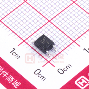
Part No. : LTV-355T-V
BNS-OD-C131/A4
Page :
1 of 11
�L ITE- O N TECH NO LO G Y CO RP O RATIO N
Property of LITE-ON Only
OUTLINE DIMENSIONS
LTV-355T-V :
*1. 2-digit date code. *2. Factory identification mark shall be marked (Z : Taiwan, Y : Thailand, X : China). *3. Rank shall be or shall not be marked.
Part No. : LTV-355T-V
BNS-OD-C131/A4
Page :
2 of 11
�L ITE- O N TECH NO LO G Y CO RP O RATIO N
Property of LITE-ON Only
TAPING DIMENSIONS
Description Tape wide Pitch of sprocket holes Distance of compartment Distance of compartment to compartment
Symbol W P0 F P2 P1
Dimensions in mm ( inches ) 12 ± 0.3 ( .47 ) 4 ± 0.1 ( .15 ) 5.5 ± 0.1 ( .217 ) 2 ± 0.1 ( .079 ) 8 ± 0.1 ( .315 )
Part No. : LTV-355T-V
BNS-OD-C131/A4
Page :
3 of 11
�L ITE- O N TECH NO LO G Y CO RP O RATIO N
Property of LITE-ON Only
ABSOLUTE MAXIMUM RATING
( Ta = 25°C )
PARAMETER Forward Current INPUT Reverse Voltage Power Dissipation Collector - Emitter Voltage Emitter - Collector Voltage OUTPUT Collector Current Collector Power Dissipation Total Power Dissipation *1 Isolation Voltage Operating Temperature Storage Temperature *2 Soldering Temperature IC PC Ptot Viso Topr Tstg Tsol 80 150 170 3,750 -55 ~ +100 -55 ~ +150 260 mA mW mW Vrms °C °C °C SYMBOL IF VR P VCEO VECO RATING 50 6 70 35 6 UNIT mA V mW V V
*1. AC For 1 Minute, R.H. = 40 ~ 60% Isolation voltage shall be measured using the following method. (1) Short between anode and cathode on the primary side and between collector and emitter on the secondary side. (2) The isolation voltage tester with zero-cross circuit shall be used. (3) The waveform of applied voltage shall be a sine wave. *2. For 10 Seconds
Part No. : LTV-355T-V
BNS-OD-C131/A4
Page :
4 of 11
�L ITE- O N TECH NO LO G Y CO RP O RATIO N
Property of LITE-ON Only
ELECTRICAL - OPTICAL CHARACTERISTICS
( Ta = 25°C )
PARAMETER Forward Voltage INPUT Reverse Current Terminal Capacitance Collector Dark Current Collector-Emitter Breakdown Voltage Emitter-Collector Breakdown Voltage Collector Current * Current Transfer Ratio Collector-Emitter Saturation Voltage Isolation Resistance Floating Capacitance Cut-Off Frequency Response Time (Rise) Response Time (Fall) SYMBOL MIN. TYP. MAX. UNIT VF IR Ct ICEO BVCEO — — — — 35 1.2 — 30 — — 1.4 10 250 1 — V µA pF µA V CONDITIONS IF=20mA VR=4V V=0, f=1KHz VCE=10V, IF=0 IC=0.1mA IF=0 IE=10µA IF=0 IF=1mA VCE=2V IF=20mA IC=5mA DC500V 40 ~ 60% R.H. V=0, f=1MHz VCE=5V, IC=2mA RL=100Ω, -3dB VCE=2V, IC=10mA RL=100Ω
OUTPUT
BVECO IC CTR VCE(sat)
6 6 600 —
— — — 0.8
— 75 7,500 1
V mA % V Ω pF kHz µs µs
TRANSFER CHARACTERISTICS
Riso Cf fc tr tf
5×10¹⁰ 1×10¹¹ — 1 — — 0.6 6 60 53
— 1 — 300 250
* CTR =
IC × 100% IF
Part No. : LTV-355T-V
BNS-OD-C131/A4
Page :
5 of 11
�L ITE- O N TECH NO LO G Y CO RP O RATIO N
Property of LITE-ON Only
ISOLATION SPECIFICATION ACCORDING TO VDE 0884
Parameter
Class of environmental test Pollution Maximum Operating Isolation Voltage Partial Discharge Diagram 1 Test Voltage (Between Input and Diagram 2 Output) Maximum Over-voltage Safety Maximum Ratings 1) Case Temperature 2) Input Current 3) Electric Power (Output or Total Power Issipation)
Symbol
VIORM
Conditions
DIN IEC68 DIN VDE0110 tp=60s, qc
很抱歉,暂时无法提供与“LTV-355T-V”相匹配的价格&库存,您可以联系我们找货
免费人工找货- 国内价格
- 5+1.56447
- 50+1.21961
- 600+0.88749
- 1200+0.87418
- 国内价格
- 5+2.25831
- 50+1.78419
- 150+1.58094
- 500+1.25215
- 国内价格
- 5+2.07584
- 50+2.0447
- 600+1.29742
- 1200+1.17943
- 国内价格
- 5+1.11005
- 50+0.87955
- 600+0.65748
- 1200+0.64762
- 3000+0.6026
- 国内价格
- 5+2.0971
- 50+1.6612
- 150+1.47431
- 国内价格
- 1+3.0282
- 10+2.4108
- 30+2.1462
- 100+1.813
- 国内价格
- 1+2.9498
- 10+2.6656
- 30+2.5186
- 国内价格
- 1+2.8314
- 10+2.2374
- 400+1.6137
- 800+1.5741
- 2000+1.55836
- 国内价格
- 10+0.396
- 20+0.39006
- 40+0.38412
- 100+0.3465
- 1000+0.3267
- 国内价格
- 5+0.61456
- 50+0.49118
- 600+0.37544
- 1200+0.36981