SPA™ Silicon Protection Array Products
Low Capacitance ESD Protection Array
HF
RoHS
Pb
GREEN
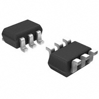
SP3003 Lead-Free/Green Series
Description The SP3003 has ultra low capacitance rail-to-rail diodes with an additional zener diode fabricated in a proprietary silicon avalanche technology to protect each I/O pin providing a high level of protection for electronic equipment that may experience destructive electrostatic discharges (ESD). These robust diodes can safely absorb repetitive ESD strikes at the maximum level specified in the IEC 61000-4-2 international standard (Level 4, ±8kV contact discharge) without performance degradation. Their very low loading capacitance also makes them ideal for protecting high speed signal pins such as HDMI, DVI, USB2.0, and IEEE 1394.
Pinout
SP3003-02X/J SP3003-04X/J
Features 0.65pF (TYP) per I/O contact discharge, ±15kV air discharge, (IEC61000-4-2) IEC61000-4-4, 40A (5/50ns)
NC NC GND NC NC
NC GND VCC
I/O 1
I/O 1 GND
I/O 4 VCC I/O 3
0.5μA (MAX) at 5V board space (SC70, SOT553, SOT563, MSOP10) IEC61000-4-5, 2.5A (8/20μs)
I/O 2
I/O 2
SP3003-04A
I/O 1 I/O 2 VCC I/O 3 I/O 4
Applications
Functional Block Diagram
SP3003-02
VCC
SP3003-04
I/O2 VCC I/O4
I/O1
I/O2
GND
I/O1
GND
I/O3
Not Intended for Use in Life Support or Life Saving Applications The products shown herein are not designed for use in life sustaining or life saving applications unless otherwise expressly indicated. SP3003 Lead-Free/Green Series
©2010 Littelfuse, Inc. Specifications are subject to change without notice. Please refer to http://www.littelfuse.com for current information.
65 Revised: August 19, 2010
Lead-Free/Green SP3003
�SPA™ Silicon Protection Array Products
Low Capacitance ESD Protection Array
Absolute Maximum Ratings
Symbol IPP TOP TSTOR Peak Current (tp=8/20μs) Operating Temperature Storage Temperature Parameter Value 2.5 -40 to 85 -50 to 150 Units A °C °C
CAUTION: Stresses above those listed in “Absolute Maximum Ratings” may cause permanent damage to the device. This is a stress only rating and operation of the device at these or any other conditions above those indicated in the operational sections of this specification is not implied.
Thermal Information
Parameter Storage Temperature Range Maximum Junction Temperature Maximum Lead Temperature (Soldering 10s) Rating -65 to 150 150 260 Units °C °C °C
Electrical Characteristics (TOP=25ºC)
Parameter Reverse Standoff Voltage Reverse Leakage Current Clamp Voltage1 Symbol VRWM ILEAK VC Test Conditions IR ≤ 1μA VR=5V IPP=1A, tp=8/20μs, Fwd IPP=2A, tp=8/20μs, Fwd IEC61000-4-2 (Contact) IEC61000-4-2 (Air) Reverse Bias=0V Reverse Bias=1.65V Reverse Bias=0V ±8 ±15 0.7 0.55 0.8 0.65 0.35 0.95 0.8 10.0 11.8 Min Typ Max 6 0.5 12.0 15.0 Units V μA V V kV kV pF pF pF
ESD Withstand Voltage1
VESD
Diode Capacitance1 Diode Capacitance
1
C CI/O-I/O
SP3003 Lead-Free/Green Series
66 Revised: August 19, 2010
©2010 Littelfuse, Inc. Specifications are subject to change without notice. Please refer to http://www.littelfuse.com for current information.
�SPA™ Silicon Protection Array Products
Low Capacitance ESD Protection Array
Insertion Loss (S21) I/O to GND
1 0 -1
Capacitance vs. Bias Voltage
1.00 0.95 0.90
I/O Capacitance (pF)
Insertion Loss [dB]
-2 -3 -4 -5 -6 -7 -8 -9 -10 1.E+06 1.E+07 1.E+08 1.E+09 1.E+10
0.85 0.80 VCC = Float 0.75 0.70 0.65 VCC = 5V 0.60 0.55 0.50 0.0 0.5 1.0 1.5 2.0 2.5 3.0 3.5 4.0 4.5 5.0 VCC = 3.3V
Frequency [Hz]
I/O DC Bias (V)
Capacitance vs. Frequency
1.4E-12
1.2E-12
Capacitance [F]
1E-12
8E-13
6E-13
4E-13
2E-13
0 1.E+06 1.E+07 1.E+08 1.E+09
Frequency [Hz]
©2010 Littelfuse, Inc. Specifications are subject to change without notice. Please refer to http://www.littelfuse.com for current information.
67 Revised: August 19, 2010
SP3003 Lead-Free/Green Series
Lead-Free/Green SP3003
�SPA™ Silicon Protection Array Products
Low Capacitance ESD Protection Array
Application Example
+5V D2+ D26 5 4 SP300x-04 1 2 3
D2+ Gnd D2-
D1+ D1HDMI or DVI Interface IC D0+ D06 5 4 SP300x-04 1 2 3
D1+ Gnd D1HDMI or DVI Connector D0+ Gnd D0-
Clk+ ClkGnd
Clk+ Gnd Clk-
HDMI or DVI application example for the Littelfuse SP300x-04 protection devices. A single 4 channel SP300x-04 device can be used to protect four of the data lines in a HDMI/DVI interface. Two (2) SP300x-04 devices provide protection for the main data lines. Low voltage
ASIC HDMI/DVI drivers can also be protected with the SP300x-04, the +VCC pins on the SP300x-04 can be substituted with a suitable bypass capacitor or in some backdrive applications the +VCC of the SP300x-04 can be
Soldering Parameters
Reflow Condition - Temperature Min (Ts(min)) Pre Heat - Temperature Max (Ts(max)) - Time (min to max) (ts) Average ramp up rate (Liquidus) Temp (TL) to peak TS(max) to TL - Ramp-up Rate Reflow - Temperature (TL) (Liquidus) - Temperature (tL) Pb – Free assembly 150°C 200°C 60 – 180 secs 3°C/second max 3°C/second max 217°C 60 – 150 seconds 250+0/-5 °C 20 – 40 seconds 6°C/second max 8 minutes Max. 260°C
Peak Temperature (TP) Time within 5°C of actual peak Temperature (tp) Ramp-down Rate Time 25°C to peak Temperature (TP) Do not exceed
SP3003 Lead-Free/Green Series
68 Revised: August 19, 2010
©2010 Littelfuse, Inc. Specifications are subject to change without notice. Please refer to http://www.littelfuse.com for current information.
�SPA™ Silicon Protection Array Products
Low Capacitance ESD Protection Array
Package Dimensions — SC70-5
e 6 5 e 4
Package Solder Pad Layout
E HE
SC70-5 5 MO-203 Issue A Millimeters Inches Min 0.031 0.000 0.028 0.006 0.003 0.073 0.045 0.079 0.010 Max 0.043 0.004 0.039 0.012 0.010 0.089 0.053 0.094 0.018 Min Max 1.10 0.10 1.00 0.30 0.25 2.25 1.35 2.40 0.46
not used
Pins JEDEC
1 B
2
3
A
D A2 A
0.80 0.00 0.70 0.15 0.08 1.85 1.15 2.00 0.26
A1 A2 B
A1
c D E
L
C
e HE L
0.65 BSC
0.026 BSC
Package Dimensions — SC70-6
e 6 5 e 4
Package Solder Pad Layout
E HE
SC70-6 6 MO-203 Issue A Millimeters Min Max 1.10 0.10 1.00 0.30 0.25 2.25 1.35 2.40 0.46 Min 0.031 0.000 0.028 0.006 0.003 0.073 0.045 0.079 0.010 Inches Max 0.043 0.004 0.039 0.010 0.089 0.053 0.094 0.018 0.012
Pins JEDEC
1 B
2
3
A
D A2 A
0.80 0.00 0.70 0.15 0.08 1.85 1.15 2.00 0.26
A1 A2 B c D E
L A1
C
e HE L
0.65 BSC
0.026 BSC
Package Dimensions — SOT553
D 6 5 4 (not used) 2 e B 3 A L
Package Pins Solder Pad Layout A Millimeters Min 0.50 0.17 0.08 1.50 1.10 0.10 1.50 B c D E e L HE
SOT 553 5 Inches Min 0.020 0.007 0.003 0.059 0.043 0.004 0.059 Max 0.024 0.011 0.007 0.067 0.051 0.012 0.067 Max 0.60 0.27 0.18 1.70 1.30 0.30 1.70
E
HE
c
0.50 BSC
0.020 BSC
©2010 Littelfuse, Inc. Specifications are subject to change without notice. Please refer to http://www.littelfuse.com for current information.
69 Revised: August 19, 2010
SP3003 Lead-Free/Green Series
Lead-Free/Green SP3003
�SPA™ Silicon Protection Array Products
Low Capacitance ESD Protection Array
Package Dimensions — SOT563
D 6 5 2 e B 4 3 A L
Package Pins Solder Pad Layout A Millimeters Min 0.50 0.17 0.08 1.50 1.10 0.10 1.50 B c D E e L HE
SOT 563 6 Inches Min 0.020 0.007 0.003 0.059 0.043 0.004 0.059 Max 0.024 0.011 0.007 0.067 0.051 0.012 0.067 Max 0.60 0.27 0.18 1.70 1.30 0.30 1.70
E
HE
c
0.50 BSC
0.020 BSC
Package Dimensions — MSOP10
Package Pins Millimeters Min A A1 B c D
Solder Pad Layout
MSOP10 10 Inches Min 0.000 0.007 0.003 0.114 0.184 0.114 0.016 Max 0.043 0.006 0.011 0.009 0.122 0.200 0.122 0.031 Max 1.10 0.15 0.27 0.23 3.10 5.10 3.10 0.80
0.00 0.17 0.08 2.90 4.67 2.90 0.40
E E1 e HE
0.50 BSC
0.020 BSC
Part Numbering System
Product Characteristics
Lead Plating
G= Green T= Tape & Reel Package
SP 3003 -04 X T G
Silicon Protection Array Series Number of Channels
Matte Tin (SC70-x, MSOP-10), Pre-Plated Frame (SOT5x3) Copper Alloy 0.0004 inches (0.102mm) Silicon Molded Epoxy UL94-V-0
Lead Material Lead Coplanarity Subsitute Material Body Material Flammability
A = MSOP-10, 3000 quantity J = SC70-5 or SC70-6, 3000 quantity -02 = 2 channel X = SOT553 or SOT563, 5000 quantity (SC70-5, SOT553 packages) -04 = 4 channel (SC70-6, SOT563, MSOP-10 packages)
Part Marking System
1. All dimensions are in millimeters
XXX XXX
Product Series
(varies) F, H or P = SP3003 series (varies)
2. Dimensions include solder plating. 3. Dimensions are exclusive of mold flash & metal burr.
Number of Channels
(varies) 2 or 4
4. All specifications comply to JEDEC SPEC MO-223 Issue A 5. Blo is facing up for mold and facing down for trim/form, i.e. reverse trim/form. 6. Package surface matte finish VDI 11-13.
Assembly Site
SP3003 Lead-Free/Green Series
70 Revised: August 19, 2010
©2010 Littelfuse, Inc. Specifications are subject to change without notice. Please refer to http://www.littelfuse.com for current information.
�SPA™ Silicon Protection Array Products
Low Capacitance ESD Protection Array
Ordering Information
Part Number SP3003-02JTG SP3003-02XTG SP3003-04ATG SP3003-04JTG SP3003-04XTG Package SC70-5 SOT553 MSOP-10 SC70-6 SOT563 Marking FX2 FX2 FX4 FX4 FX4 Min. Order Qty. 3000 5000 4000 3000 5000
Embossed Carrier Tape & Reel Specifications - SC70-5 and SC70-6
Millimetres Min E F P2 D D1 P0 10P0 W P A0 B0 K0 t 1.65 3.45 1.95 1.40 1.00 3.90 7 .70 3.90 2.14 2.24 1.12 0.27 max Max 1.85 3.55 2.05 1.60 1.25 4.10 8.10 4.10 2.34 2.44 1.32 Min 0.064 0.135 0.077 0.055 0.039 0.154 0.303 0.153 0.084 0.088 0.044 Inches Max 0.073 0.139 0.081 0.063 0.049 0.161 0.318 0.161 0.092 0.960 0.052
40.0+/- 0.20
1.574+/-0.008
Embossed Carrier Tape & Reel Specifications - SOT553 and SOT563
Millimetres Min E F P2 D D1 P0 10P0 W P A0 B0 K0 t 1.65 3.45 1.95 1.40 0.45 3.90 7 .70 3.90 1.73 1.73 0.64 0.22 max Max 1.85 3.55 2.05 1.60 0.55 4.10 8.10 4.10 1.83 1.83 0.74 Min 0.064 0.135 0.076 0.055 0.017 0.154 0.303 0.153 0.068 0.068 0.025 Inches Max 0.073 0.139 0.081 0.063 0.021 0.161 0.318 0.161 0.072 0.072 0.029
40.0+/- 0.20
1.574+/-0.008
0.009 max
©2010 Littelfuse, Inc. Specifications are subject to change without notice. Please refer to http://www.littelfuse.com for current information.
71 Revised: August 19, 2010
SP3003 Lead-Free/Green Series
Lead-Free/Green SP3003
0.010 max
�SPA™ Silicon Protection Array Products
Low Capacitance ESD Protection Array
Embossed Carrier Tape & Reel Specification - MSOP-10
Millimetres Min E F D D1 P0 10P0 W P A0 B0 K0 t 3.90 11.90 7 .90 5.20 3.20 1.20 1.65 5.40 1.50 1.50 Min 4.10 12.10 8.10 5.40 3.40 1.40 40.0+/- 0.20 Max 1.85 5.60 1.60 Min 0.065 0.213 0.059 0.154 0.469 0.311 0.205 0.126 0.047 Inches Max 0.073 0.220 0.063 0.161 0.476 0.319 0.213 0.134 0.055
0.059 Min 1.574+/-0.008
0.30 +/- 0.05
0.012+/- 0.002
SP3003 Lead-Free/Green Series
72 Revised: August 19, 2010
©2010 Littelfuse, Inc. Specifications are subject to change without notice. Please refer to http://www.littelfuse.com for current information.
�
很抱歉,暂时无法提供与“SP3003-04JTG”相匹配的价格&库存,您可以联系我们找货
免费人工找货- 国内价格
- 5+1.1696
- 20+1.0664
- 100+0.9632
- 500+0.86
- 1000+0.81184
- 2000+0.77744
- 国内价格
- 1+2.35966
- 10+2.27226
- 100+2.06252
- 500+1.95764
- 国内价格
- 1+1.56039
- 10+1.44036
- 30+1.41635
- 100+1.34433