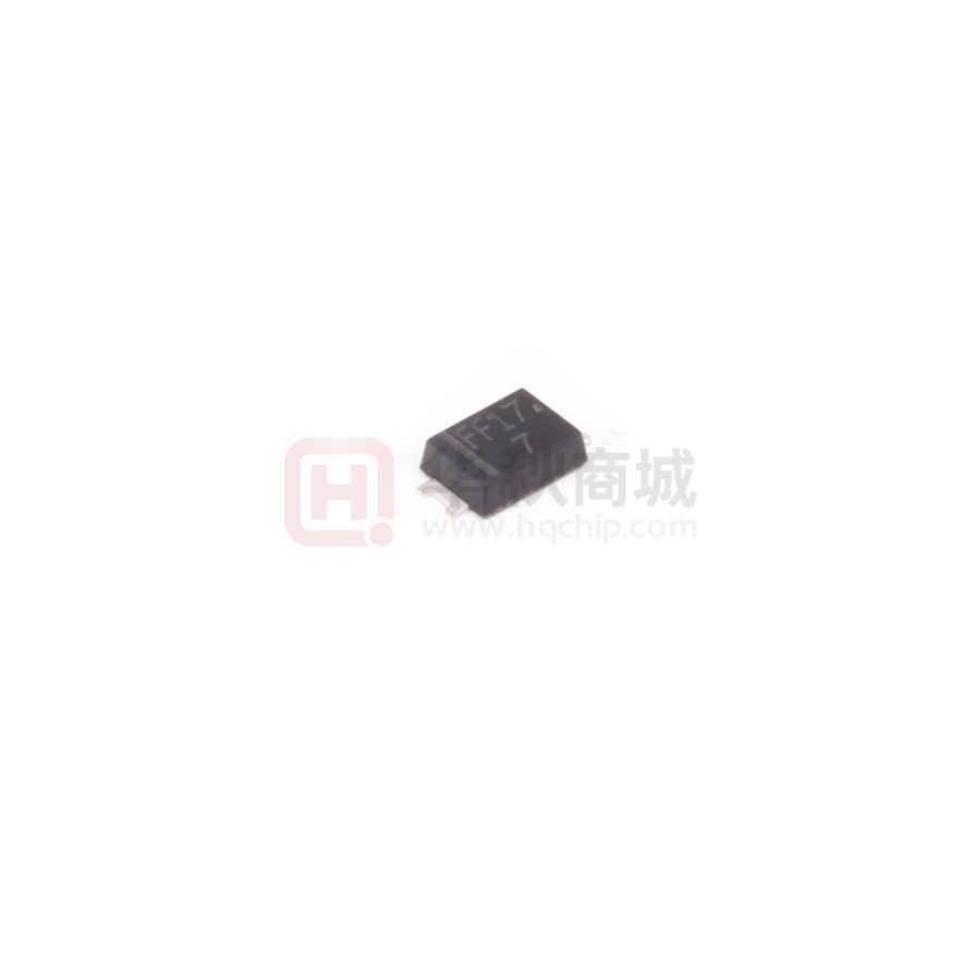
FFMAF101 thru FFMAF107T
Surface Mount Glass Passivated Junction Fast Recovery Rectifiers
Reverse Voltage 50 to 1000V Forward Current 1.0A
FEATURES
* Plastic package has Underwriters Laboratory
Flammability Classification 94V-0
* High temperature metallurgically
bonded construction
* Cavity-free glass passivated junction
* Capable of meeting environmental standards
of MIL-S-19500
* Typical IR less than 1.0µA
* High temperature soldering guaranteed:
260°C/10 seconds
Mechanical Data
Case: JEDEC SMA-FL, molded plastic over glass DIE
We declare that the material of product is
Terminals: Plated leads, solderable per
Haloggen free (green epoxy compound)
MIL-STD-750, Method 2026
Polarity: Color band denotes cathode end
Mounting Position: Any
Weight: 28mg
Handling precautin:None
Electrical Characteristic
1.Maximum & Thermal Characteristics Ratings at 25°C ambient temperature unless otherwise specified.
Parameter Symbol
symbol
Device marking code
FFMAF
101
FFMAF
102
FFMAF
103
FFMAF
104
FFMAF
105
FFMAF
106
FFMAF
107
FFMAF
107P
FFMAF
107T
FF17 FF17P FF17T
Unit
FF11
FF12
FF13
FF14
FF15
FF16
Maximum repetitive peak reverse voltage
VRRM
50
100
200
400
600
800
1000
1000
1000
V
Maximum RMS voltage
VRMS
35
70
140
280
420
560
700
700
700
V
Maximum DC blocking voltage
VDC
50
100
200
400
600
800
1000
1000
1000
V
Maximum average forward rectified current
lead length at TC = 75°C(Note 2)
IF(AV)
1.0
A
Peak forward surge current 8.3ms single half sinewave superimposed on rated load (JEDEC Method)
IFSM
30
A
Maximum reverse recovery time (Note 1)
trr
Typical thermal resistance (Note 2)
RθJA
RθJL
150
500
250
Operating junction temperature range
TJ
150
35
–55 to +150
storage temperature range
TSTG
–55 to +150
250
160
ns
°C/W
°C
°C
Electrical Characteristics Ratings at 25°C ambient temperature unless otherwise specified.
Parameter Symbol
symbol
FFMAF
101
FFMAF
102
FFMAF
103
FFMAF
104
FFMAF
105
FFMAF
106
FFMAF
107
FFMAF
107P
FFMAF
107T
Unit
Maximum instantaneous forward voltage at 1.0A
VF
1.3
V
Maximum DC reverse current TJ= 25°C
at rated DC blocking voltage TJ = 125°C
IR
5.0
100
µA
Typical junction capacitance at 4.0V, 1MHz (Note 2)
CJ
15.0
PF
NOTES:
1. IF = 0.5A, IR = 1.0A, IRR = 0.25A
2
2. 8.0mm (.013mm thick) land areas
Leshan Radio Company, LTD.
Rev.B Dec. 2019
1/3
�FFMAF101 thru FFMAF107T
2. Characteristic Curves ( TA = 25°C unless otherwise noted )
Fig. 2 – Maximum Non-repetitive Peak
Forward Surge Current
Average Forward Rectified Current (A)
Average Forward Rectified Current (A)
Fig. 1 – Forward Current Derating Curve
60 Hz
Resistive or
Inductive Load
1.0
0.5
0.375" (9.5mm) Lead Length
0
30
15
0
1
0
25 50 75 100 125 150 175
Case Temperature, °C
Fig 3. – Typical Instantaneous Forward
Characteristics
1.0
0.1
TJ = 25°C
Pulse width = 300µs
1% Duty Cycle
0.01
0.001
0.6
10
Tj=75℃
0.1
Tj=25℃
0.01
1.6
Tj=125℃
1.0
Fig 5. –typical transient thermal
impedance
0
20
40
60
80
100
Percent of Rated Peak Reverse Voltage (%)
Fig 6. – Typical Junction Capacitance
100
100
10
1
0.01
100
100
Junction Capacitance (pF)
Transient thermal impedance(°C/W)
1000
0.8
1.0
1.2
1.4
Instantaneous Forward Voltage
10
Number of Cycles at 60Hz
Fig 4. – Typical Reverse Characteristics
Instantaneous Reverse Current (µA)
Instantaneous Forward Current (A)
10
TJ = TJ max
8.3ms Single Half Sine-wave
(JEDEC Method)
0.1
1.0
10
t,Pulse duration,sec
Leshan Radio Company, LTD.
10
1.0
0.1
100
Rev.B Dec. 2019
TJ = 25°C
f = 1.0 MHz
Vsig = 50mVp-p
1
10
Reverse Voltage (V)
100
2/3
�3.OUTLINE AND DIMENSIONS
SMA-FL
MIN
MAX
4.40
4.80
2.30
2.70
3.30
3.70
DIM
Typ.
A
4.60
B
2.60
C
3.50
D
0.55
E
0.90
1.20
1.05
F
0.11
0.21
0.17
G
1.30
1.50
1.40
I
0.90
K
0.80
L
0.20
All Dimensions in mm
GENERAL NOTES
1.Top package surface finish Ra0.4±0.2um
2.Bottom package surface finish Ra0.7±0.2um
4.SOLDERING FOOTPRINT
SMA-FL
DIM
(mm)
X
1.60
Y
1.80
B
3.70
Leshan Radio Company, LTD.
Rev.B Dec. 2019
3/3
�Title: Power Packages Product Packing Specification
功率产品包装规范
Document Number: APS-QA-QS-009
Proprietary Information
Revision C
Page 3 of 6
8.1.2 Label position and QA stamp position.(Empty area) 标签张贴位置及QA印章位置。(印章盖在标
签空白区
静电敏感器件标识
7英寸卷盘标签张贴及QA印章位置
13英寸卷盘标签张贴及QA印章位置
8.1.3 Ensure direction In the same reel. The same steel coil plate direction,With antistatic bubble to
package reel。Refer to the below picture.
同一箱内的卷盘方向一致,用防静电泡沫对卷盘进行包裹。
7英寸卷盘防静电泡沫包裹
13英寸卷盘防静电泡沫包裹
Do not copy without written permission from Advanced Power Semiconductor
�Title: Power Packages Product Packing Specification
功率产品包装规范
Document Number: APS-QA-QS-009
Proprietary Information
Revision C
Page 4 of 6
8.1.4 Put in the antistatic packing box after packaged reels. And QA stamp on the box label .
将包装好的卷盘放入防静电纸箱中,并在盒标签上盖章。
7 英寸卷盘内盒及标签
8.1.5 Product use printing inner box.
13 英寸卷盘内盒及标签
产品使用LRC印字内箱。
印字内盒
印字内盒
7英寸卷盘内箱印字(侧面)
13英寸卷盘内箱印字(正面)
8.1.6 Inner box packing quantity requirement.内盒包装数量要求。
Product
Description
QTY
SOD123-FL
1-10Reels
SOD323-HE
1-10Reels
SMA-FL
1-7Reels
SMB-FL
1-4Reels
8.1.7 With transparent tape sealing. 透明胶带封箱。
Do not copy without written permission from Advanced Power Semiconductor
�Title: Power Packages Product Packing Specification
功率产品包装规范
Document Number: APS-QA-QS-009
Proprietary Information
Revision C
Page 5 of 6
7英寸内箱封盒
13英寸内箱封盒
8.1.8 Outer box size and packing quantity requirement,外箱尺寸及包装数量要求。
Product
Description
卷盘尺寸
Height(H) Width(W) Length(L)
Max. Qty
Power
Device
7 英寸
410mm
400mm
445mm
12
Power
Device
13 英寸
410mm
400mm
445mm
5
统一方向
7 英寸卷盘产品装箱
13 英寸卷盘产品装箱
Do not copy without written permission from Advanced Power Semiconductor
�Title: Power Packages Marking & Taping
Specification
功率封装字模和编带规范
Proprietary Information
Document Number:APS-QA-QS-010
Revision C
Page 6 of 9
8.2 Standard Products Taping Specification
标准产品编带规范
8.2.1 Tape length of no component
空带长度说明
Taping leader length 引导部分:440mm±40mm ,Tape trailer 尾部:200mm±40mmt
160mm-240mm
400mm-480mm
TAPE LEADER
8.2.2 Component packaging orientation: The cathode lead is close to the carrier tape’s index hole.
产品放置方向:印阴极带引脚邻近载带索引孔
Do not copy without written permission from Advanced Power Semiconductor
�Title: Power Packages Marking & Taping
Specification
功率封装字模和编带规范
Proprietary Information
Document Number:APS-QA-QS-010
Revision C
Page 7 of 9
8.2.3 Tape enwind orientation
编带缠绕方向要求
Do not copy without written permission from Advanced Power Semiconductor
�
很抱歉,暂时无法提供与“FFMAF107”相匹配的价格&库存,您可以联系我们找货
免费人工找货