LESHAN RADIO COMPANY, LTD.
Bias Resistor Transistor
NPN Silicon Surface Mount Transistor
with Monolithic Bias Resistor Network
LDTD143ELT1G
S-LDTD143ELT1G
•
Applications
Inverter, Interface, Driver
• Features
1) Built-in bias resistors enable the configuration of an
inverter circuit without connecting external input
resistors (see equivalent circuit).
2) The bias resistors consist of thin-film resistors with
complete isolation to allow positive biasing of the input.
They also have the advantage of almost completely
eliminating parasitic effects.
3) Only the on/off conditions need to be set for operation,
making the device design easy.
3
1
2
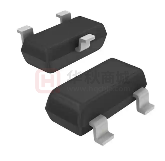
SOT-23
•
We declare that the material of product compliance with
RoHS requirements.
• S- Prefix for Automotive and Other Applications Requiring Unique Site
and Control Change Requirements; AEC-Q101 Qualified and PPAP Capable
1
BASE
zAbsolute maximum ratings (Ta=25°C)
Symbol
Limits
Unit
Supply voltage
VCC
50
V
Input voltage
VIN
−10 to +30
V
Output current
IC
500
mA
Power dissipation
PD
200
mW
Junction temperature
Tj
150
°C
Storage temperature
Tstg
−55 to +150
°C
Parameter
R1
3
COLLECTOR
R2
2
EMITTER
DEVICE MARKING AND RESISTOR VALUES
Device
Marking
R1 (K)
R2 (K)
Shipping
LDTD143ELT1G
S-LDTD143ELT1G
E6
4.7
4.7
3000/Tape & Reel
LDTD143ELT3G
S-LDTD143ELT3G
E6
4.7
4.7
10000/Tape & Reel
zElectrical characteristics (Ta=25°C)
Parameter
Symbol
Min.
Typ.
Max.
VI (off)
−
−
0.5
VI (on)
3
−
−
VO (on)
−
0.1
0.3
V
II
−
−
1.8
mA
VI=5V
IO (off)
−
−
0.5
µA
VCC=50V, VI=0V
GI
47
−
−
−
VO=5V, IO=50mA
Input resistance
R1
3.29
4.7
6.11
kΩ
−
Resistance ratio
R2 / R1
0.8
1
1.2
−
−
−
200
−
MHz
Input voltage
Output voltage
Input current
Output current
DC current gain
Transition frequency
fT ∗
Unit
V
Conditions
VCC=5V, IO=100µA
VO=0.3V, IO=20mA
IO / II=50mA / 2.5mA
VCE=10V, IE= −50mA, f=100MHz
∗ Characteristics of built-in transistor
Rev.O 1/3
�LESHAN RADIO COMPANY, LTD.
LDTD143ELT1G ;S-LDTD143ELT1G
zElectrical characteristic curves
100
10m
VO=0.3V
OUTPUT CURRENT : Io (A)
INPUT VOLTAGE : VI (on) (V)
20
10
5
Ta= −40˚C
25˚C
100˚C
2
1
500m
200m
100m
500µ 1m
5m 10m 20m
Ta=100˚C
25˚C
−40˚C
2m
1m
500µ
200µ
100µ
500m
2m
VCC=5V
5m
50
50µ
20µ
10µ
5µ
2µ
1µ
0
50m 100m 200m
0.5
OUTPUT CURRENT : IO (A)
1
VO=5V
OUTPUT VOLTAGE : VO (on) (V)
DC CURRENT GAIN : GI
2.5
3.0
lO / lI=20
500m
Ta=100˚C
25˚C
−40˚C
100
50
20
10
5
200m
100m
50m
Ta=100˚C
25˚C
−40˚C
20m
10m
5m
2m
2
1
500µ 1m
2.0
Fig.2 Output current vs. input voltage
(OFF characteristics)
500
200
1.5
INPUT VOLTAGE : VI (off) (V)
Fig.1 Input voltage vs. output current
(ON characteristics)
1k
1.0
2m
5m 10m 20m
50m 100m 200m 500m
OUTPUT CURRENT : IO (A)
Fig.3 DC current gain vs. output current
1m
500µ 1m
2m
5m 10m 20m
50m 100m 200m 500m
OUTPUT CURRENT : IO (A)
Fig.4 Output voltage vs. output current
Rev.O 2/3
�LESHAN RADIO COMPANY, LTD.
LDTD143ELT1G;S-LDTD143ELT1G
SOT-23
NOTES:
1. DIMENSIONING AND TOLERANCING PER ANSI
Y14.5M,1982
2. CONTROLLING DIMENSION: INCH.
A
L
3
1
V
2
A
B
C
D
G
H
J
G
C
D
MIN
0.1102
0.0472
0.0350
0.0150
0.0701
0.0005
INCHES
MAX
0.1197
0.0551
0.0440
0.0200
0.0807
0.0040
0.0034
0.0140
0.0350
0.0830
0.0177
0.0070
0.0285
0.0401
0.1039
0.0236
DIM
B S
H
K
J
K
L
S
V
MILLIMETERS
MIN
MAX
2.80
3.04
1.20
1.40
0.89
1.11
0.37
0.50
1.78
2.04
0.013
0.100
0.085
0.35
0.89
2.10
0.45
0.177
0.69
1.02
2.64
0.60
0.037
0.95
0.037
0.95
0.079
2.0
0.035
0.9
0.031
0.8
inches
mm
Rev.O 3/3
�
很抱歉,暂时无法提供与“LDTD143ELT1G”相匹配的价格&库存,您可以联系我们找货
免费人工找货- 国内价格
- 20+0.55560
- 100+0.33140
- 800+0.23200
- 3000+0.16570
- 6000+0.15740
- 30000+0.14580
- 国内价格
- 10+0.24981
- 100+0.19743
- 300+0.17129
- 3000+0.15164
- 6000+0.13598
- 9000+0.12809