LESHAN RADIO COMPANY, LTD.
LESD9L5.0T5G
Transient Voltage
Suppressors
LESD9L5.0T5G
S-LESD9L5.0T5G
ESD Protection Diodes with Ultra−Low
Capacitance
The ESD9L is designed to protect voltage sensitive components that
require ultra−low capacitance from ESD and transient voltage events.
Excellent clamping capability, low capacitance, low leakage, and fast
response time, make these parts ideal for ESD protection on designs
where board space is at a premium. Because of its low capacitance, it is
suited for use in high frequency designs such as USB 2.0 high speed and
antenna line applications.
2
1
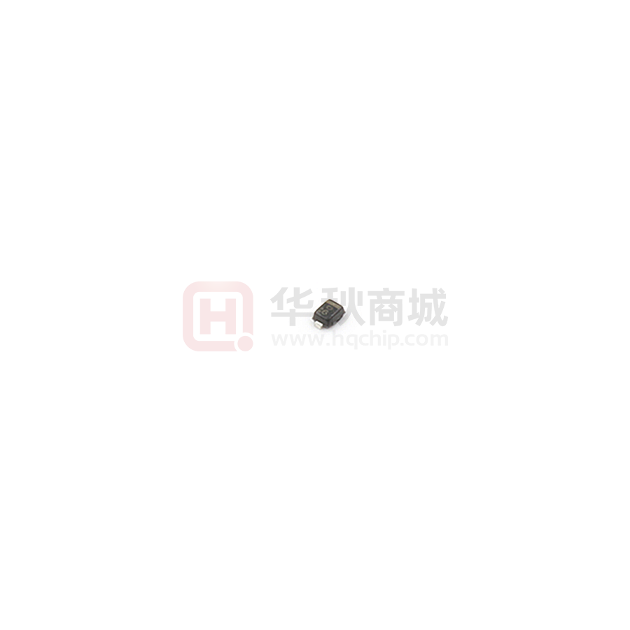
SOD-923
Specification Features:
• Ultra Low Capacitance 0.5 pF
• Low Clamping Voltage
• Small Body Outline Dimensions:
•
•
•
•
•
•
•
1
0.039″ x 0.024″ (1.00 mm x 0.60 mm)
Low Body Height: 0.016″ (0.4 mm)
Stand−off Voltage: 5 V
Low Leakage
Response Time is Typically < 1.0 ns
IEC61000−4−2 Level 4 ESD Protection
This is a Pb−Free Device
S- Prefix for Automotive and Other Applications Requiring
Unique Site and Control Change Requirements; AEC-Q101
Qualified and PPAP Capable.
2
PIN 1. CATHODE
2. ANODE
Ordering information
Device
Marking
Shipping
LESD9L5.0T5G
S-LESD9L5.0T5G
D
8000/Tape&Reel
Mechanical Characteristics:
CASE: Void-free, transfer-molded, thermosetting plastic
Epoxy Meets UL 94 V−0
LEAD FINISH: 100% Matte Sn (Tin)
QUALIFIED MAX REFLOW TEMPERATURE: 260°C
Device Meets MSL 1 Requirements
MAXIMUM RATINGS
Rating
IEC 61000−4−2 (ESD)
Symbol
Contact
Air
Value
Unit
±10
±15
kV
Total Power Dissipation on FR−5 Board
(Note 1) @ TA = 25°C
°PD°
150
mW
Storage Temperature Range
Tstg
−55 to +150
°C
Junction Temperature Range
TJ
−55 to +125
°C
Lead Solder Temperature − Maximum
(10 Second Duration)
TL
260
°C
Stresses exceeding Maximum Ratings may damage the device. Maximum
Ratings are stress ratings only. Functional operation above the Recommended
Operating Conditions is not implied. Extended exposure to stresses above the
Recommended Operating Conditions may affect device reliability.
1. FR−5 = 1.0 x 0.75 x 0.62 in.
Rev.A 1/4
�LESHAN RADIO COMPANY, LTD.
LESD9L5.0T5G , S-LESD9L5.0T5G
ELECTRICAL CHARACTERISTICS
(TA = 25°C unless otherwise noted)
Symbol
I
Parameter
IF
IPP
Maximum Reverse Peak Pulse Current
VC
Clamping Voltage @ IPP
VRWM
IR
Working Peak Reverse Voltage
VBR
Breakdown Voltage @ IT
IT
Test Current
IF
Forward Current
VF
Forward Voltage @ IF
Ppk
Peak Power Dissipation
C
VC VBR VRWM
Maximum Reverse Leakage Current @ VRWM
V
IR VF
IT
IPP
Uni−Directional TVS
Capacitance @ VR = 0 and f = 1.0 MHz
ELECTRICAL CHARACTERISTICS (TA = 25°C unless otherwise noted, VF = 1.0 V Max. @ IF = 10 mA for all types)
VRWM
(V)
IR (mA)
@ VRWM
VBR (V) @ IT
(Note 2)
IT
C (pF)
VC (V)
@ IPP = 1 A
(Note 3)
VC
Per IEC61000−4−2
(Note 4)
Device
Device
Marking
Max
Max
Min
mA
Typ
Max
Max
LESD9L5.0T5G
D
5.0
1.0
5.4
1.0
0.5
0.9
9.8
Figures 1 and 2
See Below
2. VBR is measured with a pulse test current IT at an ambient temperature of 25°C.
3. Surge current waveform per Figure 5.
4. For test procedure see Figures 3 and 4.
Figure 1. ESD Clamping Voltage Screenshot
Positive 8 kV Contact per IEC61000−4−2
Figure 2. ESD Clamping Voltage Screenshot
Negative 8 kV Contact per IEC61000−4−2
Rev.A 2/4
�LESHAN RADIO COMPANY, LTD.
LESD9L5.0T5G , S-LESD9L5.0T5G
IEC61000−4−2 Waveform
IEC 61000−4−2 Spec.
Ipeak
Level
Test
Voltage
(kV)
First Peak
Current
(A)
Current at
30 ns (A)
Current at
60 ns (A)
1
2
7.5
4
2
2
4
15
8
4
3
6
22.5
12
6
4
8
30
16
8
100%
90%
I @ 30 ns
I @ 60 ns
10%
tP = 0.7 ns to 1 ns
Figure 3. IEC61000−4−2 Spec
Oscilloscope
TVS
50 W
Cable
50 W
Figure 4. Diagram of ESD Test Setup
100
% OF PEAK PULSE CURRENT
ESD Gun
PEAK VALUE IRSM @ 8 ms
tr
90
PULSE WIDTH (tP) IS DEFINED
AS THAT POINT WHERE THE
PEAK CURRENT DECAY = 8 ms
80
70
60
HALF VALUE IRSM/2 @ 20 ms
50
40
30
tP
20
10
0
0
20
40
t, TIME (ms)
60
80
Figure 5. 8 X 20 ms Pulse Waveform
Rev.A 3/4
�LESHAN RADIO COMPANY, LTD.
LESD9L5.0T5G , S-LESD9L5.0T5G
SOD−923
D
−X−
NOTES:
1. DIMENSIONING AND TOLERANCING PER ANSI
Y14.5M, 1982.
2. CONTROLLING DIMENSION: MILLIMETERS.
3. MAXIMUM LEAD THICKNESS INCLUDES LEAD
FINISH THICKNESS. MINIMUM LEAD
THICKNESS IS THE MINIMUM THICKNESS OF
BASE MATERIAL.
−Y−
E
1
b
2
2X
0.08 (0.0032) X Y
DIM
A
b
c
D
E
HE
L
A
c
L
HE
MILLIMETERS
MIN
NOM MAX
0.34
0.37
0.40
0.15
0.20
0.25
0.07
0.12
0.17
0.75
0.80
0.85
0.55
0.60
0.65
0.95
1.00
1.05
0.05
0.10
0.15
MIN
0.013
0.006
0.003
0.030
0.022
0.037
0.002
INCHES
NOM
0.015
0.008
0.005
0.031
0.024
0.039
0.004
MAX
0.016
0.010
0.007
0.033
0.026
0.041
0.006
SOLDERING FOOTPRINT*
0.90
0.40
0.30
DIMENSIONS: MILLIMETERS
Rev.A 4/4
�
很抱歉,暂时无法提供与“LESD9L5.0T5G”相匹配的价格&库存,您可以联系我们找货
免费人工找货- 国内价格
- 20+0.19851
- 200+0.15660
- 600+0.13338
- 2000+0.11945
- 国内价格
- 20+0.37890
- 100+0.22610
- 1000+0.15820
- 8000+0.11300
- 16000+0.10740
- 80000+0.09950
- 国内价格
- 20+0.19233
- 800+0.12298
- 3200+0.12114
