LMBT3904WT1G
S-LMBT3904WT1G
General Purpose Transistors NPN Silicon
1. FEATURES
●
We declare that the material of product compliance with
RoHS requirements and Halogen Free.
●
S- prefix for automotive and other applications requiring
unique site and control change requirements; AEC-Q101
SC70(SOT-323)
qualified and PPAP capable.
2. DEVICE MARKING AND ORDERING INFORMATION
Device
Marking
Shipping
3 COLLECTOR
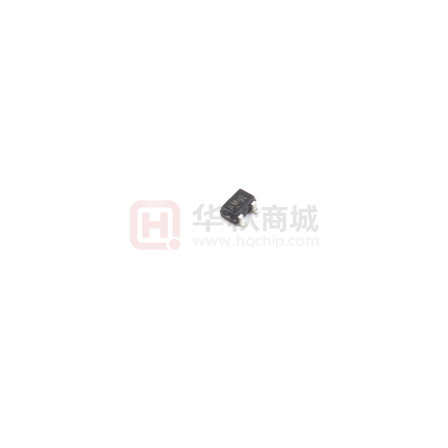
LMBT3904WT1G
AM
3000/Tape&Reel
LMBT3904WT3G
AM
10000/Tape&Reel
1 BASE
2 EMITTER
3. MAXIMUM RATINGS(Ta = 25ºC)
Symbol
Limits
Unit
Collector–Emitter Voltage
Parameter
VCEO
40
Vdc
Collector–Base Voltage
VCBO
60
Vdc
Emitter–Base Voltage
VEBO
6
Vdc
IC
200
mAdc
Symbol
Limits
Unit
Collector Current — Continuous
4. THERMAL CHARACTERISTICS
Parameter
Total Device Dissipation,
PD
FR−5 Board (Note 1) @ TA = 25ºC
150
mW
Derate above 25ºC
1.2
mW/ºC
833
ºC/W
Thermal Resistance,
RΘJA
Junction–to–Ambient(Note 1)
Junction and Storage temperature
TJ,Tstg
−55∼+150 ºC
1. FR–5 = 1.0×0.75×0.062 in.
Leshan Radio Company, LTD.
Rev.B Mar 2016
1/5
�LMBT3904WT1G, S-LMBT3904WT1G
General Purpose Transistors NPN Silicon
5. ELECTRICAL CHARACTERISTICS (Ta= 25ºC)
OFF CHARACTERISTICS
Symbol
Characteristic
Collector–Emitter Breakdown Voltage
VBR(CEO)
(IC = 1.0 mAdc, IB = 0)
Collector–Base Breakdown Voltage
VBR(CBO)
(IC = 10 μAdc, IE = 0)
Emitter–Base Breakdown Voltage
VBR(EBO)
(IE = 10 μAdc, IC = 0)
Collector Cutoff Current
ICEX
( VCE = 30 Vdc, VEB = 3.0Vdc)
Base Cutoff Current
IBL
Min.
Typ.
Max.
40
-
V
60
-
V
6
-
nA
-
-
50
nA
-
-
50
40
-
-
(IC = 1.0 mAdc, VCE = 1.0 Vdc)
70
-
-
(IC = 10 mAdc, VCE = 1.0 Vdc)
100
-
300
(IC = 50 mAdc, VCE = 1.0 Vdc)
60
-
-
30
-
-
(IC = 10 mAdc, IB = 1.0 mAdc)
-
-
0.2
(IC = 50 mAdc, IB = 5.0 mAdc)
-
-
0.3
(VCE = 30 Vdc, VEB = 3.0Vdc)
Unit
V
ON CHARACTERISTICS (Note 2.)
HFE
DC Current Gain
(IC = 0.1 mAdc, VCE = 10 Vdc)
(IC = 100 mAdc, VCE = 1.0 Vdc)
Collector–Emitter Saturation Voltage
VCE(sat)
Base–Emitter Saturation Voltage
V
VBE(sat)
V
(IC = 10 mAdc, IB = 1.0 mAdc)
0.65
-
0.85
(IC = 50 mAdc, IB = 5.0 mAdc)
-
-
0.95
SMALL–SIGNAL CHARACTERISTICS
Current–Gain — Bandwidth Product
fT
(IC = 10mAdc, VCE= 20Vdc, f = 100MHz)
Output Capacitance
Cobo
(VCB = 5.0 Vdc, IE = 0, f = 1.0 MHz)
Input Capacitance
Cibo
(VEB = 0.5 Vdc, IC = 0, f = 1.0 MHz)
MHz
300
-
pF
-
-
4
pF
-
-
8
SWITCHING CHARACTERISTICS
Delay Time
Rise Time
Storage Time
Fall Time
(VCC = 3.0 Vdc,VBE=-0.5Vdc,
IC = 10mAdc, IB1 = 1.0 mAdc)
td
-
-
35
tr
-
-
35
(VCC = 3.0 Vdc, IC = 10
mAdc,IB1 = IB2 = 1.0 mAdc)
ts
-
-
200
tf
-
-
50
ns
2.Pulse Test: Pulse Width ≤300 μs, Duty Cycle ≤2.0%.
Leshan Radio Company, LTD.
Rev.B Mar 2016
2/5
�LMBT3904WT1G, S-LMBT3904WT1G
General Purpose Transistors NPN Silicon
6.ELRCTRICAL CHARACTERISTICS CURVES
400
10
150℃
Cibo
HFE, DC Current Gain
C,Capacitance(pF)
300
Cobo
25℃
200
-55℃
100
1
0.01
0
0.1
1
10
VR.Verse Voltage(V)
0.1
100
1.0
10.0
IC,Collector Current (mA)
DC Current Gain
Capacitance
2.5
1.4
VBE(sat),Base Emitter Saturation Voltage(V)
IC/IB=10
VCE(sat), Collector-emitter Saturation(V)
100.0
2.0
150℃
1.5
1.0
25℃
0.5
-55℃
0.0
0.001
0.01
0.1
IC, Collector Current(A)
1
IC/IB=10
1.2
1
-55℃
0.8
25℃
0.6
150℃
0.4
0.2
0
0.0001
1
VBE(sat) vs. IC
VCE(sat) vs. IC
Leshan Radio Company, LTD.
0.001
0.01
0.1
IC, Collector Current(A)
Rev.B Mar 2016
3/5
�LMBT3904WT1G, S-LMBT3904WT1G
General Purpose Transistors NPN Silicon
1
1.4
1.2
VCE, Collecter Emitter Voltage(V)
VBE(on), Base-emitter Voltage(V)
VCE=1V
1
0.8
-55℃
25℃
0.6
0.4
150℃
0.8
IC=30mA
0.6
IC=10mA
IC=100mA
0.4
0.2
0.2
IC=1mA
0
0.0001
0.001
0.01
0.1
IC, Colletor Current(A)
1
0
0.001
10
Collector Saturation Region
VBE(on) vs. IC
Leshan Radio Company, LTD.
0.01
0.1
1
IB, Base Current(mA)
Rev.B Mar 2016
4/5
�LMBT3904WT1G, S-LMBT3904WT1G
General Purpose Transistors NPN Silicon
7.OUTLINE AND DIMENSIONS
Notes:
1. DIMENSIONING AND TOLERANCING PER ANSI
Y14.5M, 1982.
2. CONTROLLING DIMENSION: MILLIMETERS.
3. MAXIMUM LEAD THICKNESS INCLUDES LEAD
FINISH. MINIMUM LEAD THICKNESS IS THE MINIMUM
THICKNESS OF BASE MATERIAL.
4. DIMENSIONS D AND E DO NOT INCLUDE MOLD
FLASH, PROTRUSIONS OR GATE BURRS.
MILLIMETERS
INCHES
DIM MIN
A 0.80
A1
0.00
A2
NOM
MAX
0.90
1.00
0.032 0.035 0.039
0.05
0.10
0.000 0.002 0.004
0.70REF
MIN
NOM
MAX
0.028REF
b
0.30
0.35
0.40
0.012 0.014 0.016
c
0.10
0.18
0.25
0.004 0.007 0.010
D
1.80
2.10
2.20
0.071 0.083 0.087
E
1.15
1.24
1.35
0.045 0.049 0.053
e
1.20
1.30
1.40
0.047 0.051 0.055
e1
L
HE
0.65REF
0.026REF
0.20
0.38
0.56
0.008 0.015 0.022
2.00
2.10
2.40
0.079 0.083 0.095
8.SOLDERING FOOTPRINT
Leshan Radio Company, LTD.
Rev.B Mar 2016
5/5
�