LESHAN RADIO COMPANY, LTD.
Dual General Purpose Transistors
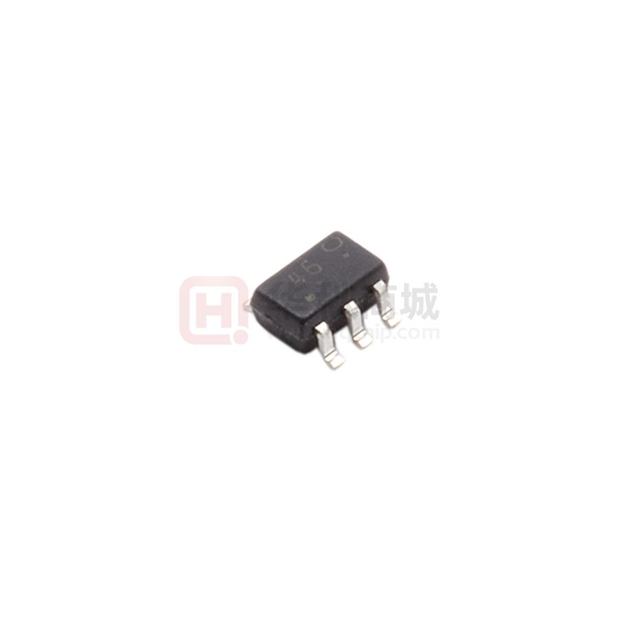
The LMBT3946DW1T1 device is a spin–off of our popular SOT–23/SOT–323 three–leaded device. It is designed for general purpose amplifier applications and is housed in the SOT–363 six–leaded surface mount package. By putting two discrete devices in one package, this device is ideal for low–power surface mount applications where board space is at a premium. • hFE, 100–300 • Low VCE(sat), < 0.4 V • Simplifies Circuit Design • Reduces Board Space • Reduces Component Count • Available in 8 mm, 7–inch/3,000 Unit Tape and Reel • Device Marking: LMBT3946DW1T1G = 46 MAXIMUM RATINGS Rating Collector-Emitter Voltage (NPN) (PNP) Collector-Base Voltage (NPN) (PNP) Emitter-Base Voltage (NPN) (PNP) Collector Current-Continuous (NPN) (PNP) Electrostatic Discharge Symbol V CEO Value 40 -40 V
CBO
LMBT3946DW1T1G
6 5 4
1 2 3
SOT-363/SC-88
We declare that the material of product compliance with RoHS requirements.
3 2 1
Unit Vdc
Q1
Q2
Vdc 60 -40
4 5 6
LMBT3946DW1T1*
V EBO 6.0 -5.0 IC 200 -200 HBM>16000, MM>2000 Max 150 833 –55 to +150
Vdc
*Q1 PNP Q2 NPN
mAdc
ORDERING INFORMATION Device Marking Shipping
LMBT3946DW1T1G LMBT3946DW1T3G 46 46 3000Units/Reel 10000Units/Reel
ESD
V
THERMAL CHARACTERISTICS Characteristic Symbol (1) Total Package Dissipation PD T A = 25°C Thermal Resistance Junction Rθ JA to Ambient Junction and Storage Temperature Range TJ,Ts t g
Unit mW °C/W °C
1. Device mounted on FR4 glass epoxy printed circuit board using the minimum 1. recommended footprint.
1/14
�LESHAN RADIO COMPANY, LTD.
LMBT3946DW1T1G
ELECTRICAL CHARACTERISTICS(TA=25°C unless otherwise noted) Characteristic Symbol OFF CHARACTERISTICS Collector–Emitter Breakdown Voltage(2) (IC = 1.0 mAdc, IB = 0) (IC = –1.0 mAdc, IB = 0) Collector–Base Breakdown Voltage (IC = 10 µAdc, IE = 0) (IC = –10 µAdc, IE = 0) Emitter–Base Breakdown Voltage (IE = 10 µAdc, IC = 0) (IE = –10 µAdc, IC = 0) Base Cutoff Current (VCE = 30 Vdc, VEB = 3.0 Vdc) (VCE = –30 Vdc, VEB = –3.0 Vdc) Collector Cutoff Current (VCE = 30 Vdc, VEB = 3.0 Vdc) (VCE = –30 Vdc, VEB = –3.0 Vdc) ON CHARACTERISTICS (2) DC Current Gain (IC = 0.1 mAdc, VCE = 1.0 Vdc) (IC = 1.0 mAdc, VCE = 1.0 Vdc) (IC = 10 mAdc, VCE = 1.0 Vdc) (IC = 50 mAdc, VCE = 1.0 Vdc) (IC = 100 mAdc, VCE = 1.0 Vdc) (IC = –0.1 mAdc, VCE = –1.0 Vdc) (IC = –1.0 mAdc, VCE = –1.0 Vdc) (IC = –10 mAdc, VCE = –1.0 Vdc) (IC = –50 mAdc, VCE = –1.0 Vdc) (IC = –100 mAdc, VCE = –1.0 Vdc) Collector–Emitter Saturation Voltage (IC = 10 mAdc, IB = 1.0 mAdc) (IC = 50 mAdc, IB = 5.0 mAdc) (IC = –10 mAdc, IB = –1.0 mAdc) (IC = –50 mAdc, IB = –5.0 mAdc) Base–Emitter Saturation Voltage (IC = 10 mAdc, IB = 1.0 mAdc) (IC = 50 mAdc, IB = 5.0 mAdc) (IIC = –10 mAdc, IB = –1.0 mAdc) (IC = –50 mAdc, IB = –5.0 mAdc) (NPN) (PNP) (NPN) (PNP) VBE(sat) 0.65 – –0.65 – 0.85 0.95 –0.85 –0.95 (NPN) (NPN) (PNP) (NPN) (PNP) ICEX – – 50 –50 (NPN) (PNP) IB L – – 50 –50 nAdc Min Max Unit
V(BR)CEO (NPN) (PNP) V(BR)CBO (NPN) (PNP) V (BR)EBO 6.0 –5.0 – – 60 –40 – – 40 –40 – –
Vdc
Vdc
Vdc
nAdc
hFE 40 70 100 60 30 60 80 100 60 30 V CE(sat) – – – – 0.2 0.3 –0.25 –0.4 – – 300 – – – – 300 – –
–
(PNP)
Vdc
Vdc
2. Pulse Test: Pulse Width < 300 µs; Duty Cycle
很抱歉,暂时无法提供与“LMBT3946DW1T1G”相匹配的价格&库存,您可以联系我们找货
免费人工找货- 国内价格
- 20+0.30730
- 100+0.18330
- 800+0.12830
- 3000+0.09170
- 6000+0.08710
- 30000+0.08060
- 国内价格
- 20+0.08850
- 200+0.08260
- 600+0.07670
- 3000+0.07080
