LESHAN RADIO COMPANY, LTD.
20V N-Channel Enhancement-Mode MOSFET
VDS= 20V
RDS(ON), Vgs@4.5V, Ids@5.0A = 41mΩ
RDS(ON), Vgs@2.5V, Ids@4.5A = 47mΩ
Features
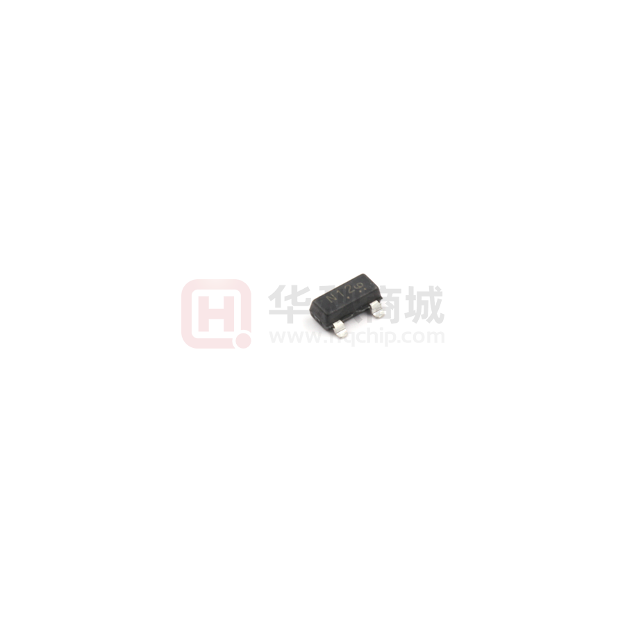
LN2312LT1G
S-LN2312LT1G
3
Advanced trench process technology
High Density Cell Design For Ultra Low On-Resistance
1
we declare that the material of product
2
compliance with RoHS requirements.
SOT– 23 (TO–236AB)
S- Prefix for Automotive and Other Applications Requiring
Unique Site and Control Change Requirements; AEC-Q101
Qualified and PPAP Capable.
D
▼ Capable of 2.5V gate drive
▼ Lower on-resistance
▼ Surface mount package
G
S
Ordering Information
Device
LN2312LT1G
S-LN2312LT1G
LN2312LT3G
S-LN2312LT3G
Marking
Shipping
N12
3000/Tape&Reel
N12
10000/Tape&Reel
Absolute Maximum Ratings
Symbol
Parameter
VDS
Drain-Source Voltage
VGS
Gate-Source Voltage
ID@TA=25℃
ID@TA=70℃
Rating
Units
20
V
±8
V
3
4.9
A
3
3.4
A
15
A
Continuous Drain Current , VGS @ 4.5V
Continuous Drain Current , VGS @ 4.5V
1,2
IDM
Pulsed Drain Current
PD@TA=25℃
Total Power Dissipation
0.75
W
Linear Derating Factor
1.3
W/℃
TSTG
Storage Temperature Range
-55 to 150
℃
TJ
Operating Junction Temperature Range
-55 to 150
℃
Thermal Data
Symbol
Rthj-a
Parameter
Thermal Resistance Junction-ambient
3
Max.
Value
Unit
140
℃/W
Rev .O 1/5
�LESHAN RADIO COMPANY, LTD.
LN2312LT1G , S-LN2312LT1G
Electrical Characteristics@Tj=25oC(unless otherwise specified)
Parameter
Static
Drain-Source Breakdown Voltage
Symbol
Test Condition
Min
Typ
Max
Unit
BVDSS
VGS = 0V, ID = 250uA
20
-
-
V
Drain-Source On-State Resistance
RDS(on)
VGS = 1.8V, ID = 4.0A
31
57
Drain-Source On-State Resistance
RDS(on)
VGS = 2.5V, ID = 4.5A
24
47
Drain-Source On-State Resistance
RDS(on)
VGS = 4.5V, ID = 5A
21
41
Gate Threshold Voltage
VGS(th)
VDS =VGS, ID = 250uA
0.6
1
V
Zero Gate Voltage Drain Current
IDSS
VDS = 20V, VGS = 0V
1
uA
Gate Body Leakage
Gate Resistance
Forward Transconductance
IGSS
Rg
gfs
VGS = +8V, VDS = 0V
+ 100
nA
Dynamic
Total Gate Charge
Gate-Source Charge
Qg
Qgs
Gate-Drain Charge
Qgd
Turn-On Delay Time
td(on)
Turn-On Rise Time
tr
Turn-Off Delay Time
td(off)
Turn-Off Fall Time
tf
Input Capacitance
Ciss
Output Capacitance
Coss
Reverse Transfer Capacitance
Source-Drain Diode
Max. Diode Forward Current
Crss
IS
Diode Forward Voltage
VSD
VDS = 10V, ID = 5A
VDS = 10V, I D = 5A
VGS = 4.5V
VDD = 10V,
ΙD = 1Α, VGEN = 4.5V
RG = 6Ω
VDS = 8V, V GS = 0V
f = 1.0 MHz
IS = 1.7A, VGS = 0V
0.4
mΩ
40
S
11.2
1.4
nC
2.2
15
40
48
31
500
25
60
70
45
ns
pF
300
140
1.7
A
1.2
V
Notes:
1.Pulse width limited by Max. junction temperature.
2.Pulse width
很抱歉,暂时无法提供与“LN2312LT1G”相匹配的价格&库存,您可以联系我们找货
免费人工找货- 国内价格
- 1+0.29920
- 200+0.19250
- 1500+0.16830
- 3000+0.14740
- 国内价格
- 20+0.69980
- 100+0.41740
- 800+0.29220
- 3000+0.20870
- 6000+0.19830
- 30000+0.18370
- 国内价格
- 10+0.34960
- 100+0.28016
- 300+0.24549
- 国内价格
- 10+0.32046
- 100+0.25681
- 600+0.25424
- 1200+0.24916
- 3000+0.24169