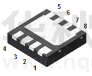
LN8544DT1AG
N-Channel 30-V (D-S) MOSFET
1. FEATURES
●
Low Gate Charge
●
High Current Capability
We declare that the material of product are Halogen Free and
compliance with RoHS requirements.
●
2. APPLICATION
●
DC/DC Converters in Computing, Servers, and POL
●
Isolated DC/DC Converters in Telecom and Industrial
3. ORDERING INFORMATION
Device
Marking
Shipping
LN8544DT1AG
854
3000/Tape&Reel
4. MAXIMUM RATINGS(Ta = 25ºC unless otherwise stated)
Drain−to−Source Voltage
Symbol
VDSS
Limits
30
Unit
V
Gate−to−Source Voltage
VGS
±20
V
IAS
31
A
EAS
48
mJ
Parameter
Avalanche Current
Avalanche energy L=0.1mH
TC =25°C
Continuous Drain Current(Note 1)
TC =70°C
TA =25°C
47
ID
IDM
TC =25°C
Maximum Power Dissipation(Note 1)
TC =70°C
TA =25°C
16
64
A
20
PD
13
2.5
W
1.6
TA =70°C
TJ
−55 ~+150
Storage Temperature Range
Tstg
−55 ~+150
Thermal Resistance-Junction to Ambient(Note 1)
RθJA
50
Thermal Resistance-Junction to Case(Note 1)
RθJC
6
Operating Junction Temperature
A
13
TA =70°C
Pulsed Drain Current
38
ºC
ºC/W
1.The device mounted on 1in ²FR4 board with 2 oz copper
Leshan Radio Company, LTD.
Rev.G Mar. 2022
1/5
�LN8544DT1AG
N-Channel 30-V (D-S) MOSFET
5. ELECTRICAL CHARACTERISTICS
Characteristic
Symbol
Min.
Typ.
Max.
Unit
V(BR)DSS
30
-
-
V
VGS(th)
1
-
2.1
V
IGSS
-
-
±100
nA
IDSS
-
-
1
μA
RDS(on)
-
3.7
5.6
mΩ
-
5.4
7.6
VSD
-
0.7
1.2
Qg
-
54
-
Static
Drain-Source Breakdown Voltage
(VGS = 0 V, ID = 250 μA)
Gate Threshold Voltage
(VDS = VGS , ID = 250 μA)
Gate Leakage Current
(VDS = 0 V, VGS = ±20 V)
Zero Gate Voltage Drain Current
(VDS = 30 V, VGS =0V)
Drain-Source On-Resistance(Note 2)
(VGS = 10 V, ID = 20 A)
(VGS = 4.5 V, ID = 16 A)
Diode Forward Voltage
(IS = 1.0 A, VGS = 0 V)
Dynamic
Total Gate Charge
(VDS = 15 V, VGS = 10 V, ID = 20 A)
Total Gate Charge
Gate-Source Charge
Gate-Drain Charge
(VDS = 15 V,
VGS = 4.5 V, ID
= 20 A)
Input Capacitance
(VDS = 15 V,
VGS
Output Capacitance
=
0
V,F=
1MHz)
Reverse Transfer Capacitance
Turn-On Delay Time
Rise Time
Turn-Off Delay Time
Fall Time
(VDD = 15 V, RL
= 15 Ω,VGEN =
10 V, RG = 3 Ω)
Qg
-
27
-
Qgs
-
9.5
-
Qgd
-
11
-
Ciss
-
2450
-
Coss
-
393
-
Crss
td(on)
-
129
23
tr
-
16
-
td(off)
-
73
-
tf
-
12
-
V
nC
pF
ns
2.Pulse test: pulse width≤300us, duty cycle≤2%, Guaranteed by design, not subject to production testing.
Leshan Radio Company, LTD.
Rev.G Mar. 2022
2/5
�LN8544DT1AG
N-Channel 30-V (D-S) MOSFET
6. ELECTRICAL CHARACTERISTICS CURVES
25
15
VGS=3V,3.5V,4V
VDS=10V
20
ID,Drain Current(A)
ID,Drain Current(A)
12
VGS=2.8V
9
6
VGS=2.6V
25℃
15
10
150℃
-55℃
5
3
VGS=2.4V
0
0
0
1
2
3
VDS,Drain to Source voltage(V)
0.0
4
1.0
2.0
3.0
VGS,Gate to Source Voltage(V)
ID vs. VGS
ID vs. VDS
7
100
10
1
150℃
25℃
RDS(on) (mΩ)
IS Diode Forward Current(A)
6
-55℃
VGS=4.5V
5
4
VGS=10V
3
2
0.1
1
0.01
0
0.2
0.4
0.6
0.8
1.0
VSD,Diode Forward Current(V)
12
14
16
18
ID,Drain Current(A)
20
RDS(on) vs. ID
IS vs. VSD
Leshan Radio Company, LTD.
10
Rev.G Mar. 2022
3/5
�LN8544DT1AG
N-Channel 30-V (D-S) MOSFET
6. ELECTRICAL CHARACTERISTICS CURVES(Con.)
35
10
RDS(on) On Resistance (mΩ)
RDS(On) ON Resistance (mΩ)
ID=20A
30
25
20
15
10
150℃
25℃
5
8
VGS=4.5V,ID=16A
6
4
VGS=10V,ID=20A
2
-55℃
0
0
2
4
6
8
VGS,Gate to Source Voltage(V)
10
-50
-25
0
RDS(on) vs. VGS
RDS(on) vs. Tj
4000
2.0
ID=250uA
f=1.0MHz
Ta=25℃
3500
1.8
3000
Ciss
1.6
Capacitance(pF)
VGSTH Threshod Voltage (V)
25
50
75 100 125 150
Tj,Temperature(℃)
1.4
1.2
2500
2000
1500
1000
1.0
Coss
500
Crss
0.8
0
-50
-25
0
25
50
75
100
125
150
0
Tj,Temperature(℃)
20
30
VDS,Drain to Source Voltage(V)
Capacitance
VGSTH vs. Tj
Leshan Radio Company, LTD.
10
Rev.G Mar. 2022
4/5
�LN8544DT1AG
N-Channel 30-V (D-S) MOSFET
7.OUTLINE AND DIMENSIONS
D1
D
e
L
Dim
A
E1
A1
b
b1
b2
D
E
D1
E1
e
L
L1
L2
A3
L1
b
b1
L2
E
C0.2
b2
BOTTOM VIEW
A
A1
A3
TOP VIEW
DFN3030-8B
Min
Nor
0.60
0.65
0.00
0.03
0.30
0.35
0.40
0.45
0.50
0.55
2.95
3.00
2.95
3.00
2.45
2.50
1.45
1.50
0.65BSC
Max
0.70
0.05
0.40
0.50
0.60
3.05
3.05
2.55
1.55
0.45
0.44
0.57
0.55
0.50
0.49
0.54
0.62
0.67
0.152REF.
All Dimensions in mm
SIDE VIEW
8.SOLDERING FOOTPRINT
X3
Y2
Y1
DFN3030-8B
C
C
Y
C1
X
X1
Leshan Radio Company, LTD.
X2
X1
Dim
C
C1
X
X1
X2
X3
Y1
Y2
Y
Rev.G Mar. 2022
(mm)
0.65
0.70
0.60
0.40
0.50
2.80
2.20
3.20
0.82
5/5
�DISCLAIMER
●
Curve guarantee in the specification. The curve of test items with electric parameter is used as quality guarantee.
The curve of test items without electric parameter is used as reference only.
●
Before you use our Products for new Project, you are requested to carefully read this document and fully under-stand its contents. LRC shall not be in any way responsible or liable for failure, malfunction or accident arising
from the use of any LRC’s Products against warning, caution or note contained in this document.
●
All information contained in this document is current as of the issuing date and subject to change without any prior
notice. Before purchasing or using LRC's Products,please confirm the latest information with a LRC sales represe-ntative.
�
很抱歉,暂时无法提供与“LN8544DT1AG”相匹配的价格&库存,您可以联系我们找货
免费人工找货