LESHAN RADIO COMPANY, LTD.
20V P-Channel Enhancement-Mode MOSFET
LP3415ELT1G
S-LP3415ELT1G
VDS= -20V
RDS(ON), Vgs@-4.5V, Ids@-4A = 60 mΩ
RDS(ON), Vgs@-2.5V, Ids@-4A = 75 mΩ
RDS(ON), Vgs@-1.8V, Ids@-2A = 85 mΩ
3
Features
Advanced trench process technology
1
High Density Cell Design For Ultra Low On-Resistance
2
we declare that the material of product
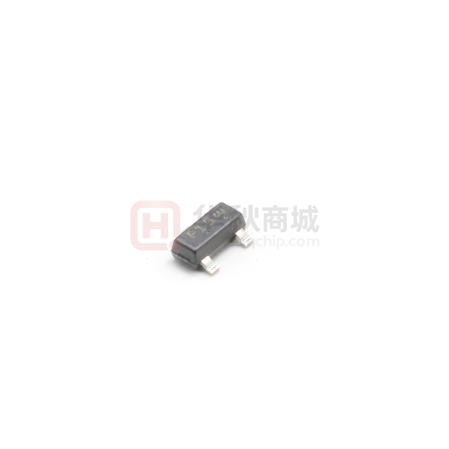
SOT– 23 (TO–236AB)
compliance with RoHS requirements.
S- Prefix for Automotive and Other Applications Requiring
Unique Site and Control Change Requirements; AEC-Q101
Qualified and PPAP Capable.
▼ Simple Drive Requirement
▼ Small Package Outline
▼ Surface Mount Device
Ordering Information
Device
Shipping
Marking
LP3415ELT1G
S-LP3415ELT1G
LP3415ELT3G
S-LP3415ELT3G
P15
3000/Tape& Reel
P15
10000/Tape& Reel
Maximum Ratings and Thermal Characteristics (TA= 25oC unless otherwise noted)
Symbol
Limit
Drain-Source Voltage
VDS
-20
Gate-Source Voltage
VGS
±8
Continuous Drain Current
ID
-4
Pulsed Drain Current 1)
IDM
-30
Parameter
o
Maximum Power Dissipation
TA = 25 C
PD
o
TA = 75 C
V
A
1
W
0.6
Operating Junction and Storage Temperature Range
Junction-to-Case Thermal Resistance
Junction-to-Ambient Thermal Resistance (PCB mounted)
Unit
2)
TJ, Tstg
-55 to 150
RqJC
100
RqJA
150
o
o
C
C/W
Note: 1. Repetitive Rating: Pulse width limited by the Maximum junction temperation
2. 1-in2 2oz Cu PCB board
3. Guaranteed by design; not subject to production testing
Rev .A 1/3
�LESHAN RADIO COMPANY, LTD.
LP3415ELT1G , S-LP3415ELT1G
ELECTRICAL CHARACTERISTICS
Parameter
Test Condition
Symbol
Min
Typ
Max
Unit
Static
Drain-Source Breakdown Voltage
BVDSS
VGS = 0V, ID = -250uA
Drain-Source On-State Resistance
RDS(on)
VGS = -1.8V, ID = -2A
85.0
Drain-Source On-State Resistance
RDS(on)
VGS = -2.5V, ID = -4A
75.0
Drain-Source On-State Resistance
RDS(on)
VGS = -4.5V, ID = -4A
60.0
Gate Threshold Voltage
VGS(th)
VDS =VGS, ID = -250uA
Zero Gate Voltage Drain Current
IDSS
Gate Body Leakage
Gate Resistance
-20
V
-0.3
mΩ
-1
V
VDS = -16V, VGS = 0V
-1
uA
IGSS
VGS = ± 8V, V DS = 0V
±10
uA
Rg
VDS = 0V, f = 1.0MHz
Ω
6.5
3)
Dynamic
Total Gate Charge
Qg
Gate-Source Charge
Qgs
Gate-Drain Charge
Qgd
Turn-On Delay Time
td(on)
Turn-On Rise Time
tr
Turn-Off Delay Time
td(off)
Turn-Off Fall Time
tf
Input Capacitance
Ciss
Output Capacitance
Coss
Reverse Transfer Capacitance
Crss
VDS =-10V, ID = -4A
VGS = -4.5V
VDD = -10V, RL = 2.5Ω
ID = -1A, VGEN = -4.5V
RG = 3Ω
4.59
5.97
2.14
2.78
2.51
3.26
965.2
1930.4
1604
3208
7716
15432
3452
6904
nC
ns
36.45
VDS = -10V, VGS = 0V
f = 1.0 MHz
pF
128.57
15.17
Source-Drain Diode
Max. Diode Forward Current
Diode Forward Voltage
IS
VSD
IS = -1A, VGS = 0V
-2.2
A
-1
V
Note: Pulse test: pulse width
很抱歉,暂时无法提供与“LP3415ELT1G”相匹配的价格&库存,您可以联系我们找货
免费人工找货- 国内价格
- 5+0.39396
- 50+0.38805
- 600+0.38417
- 1200+0.37649
- 3000+0.36520
- 国内价格
- 1+0.35200
- 200+0.22770
- 1500+0.19800
- 3000+0.17490
- 国内价格
- 20+1.23270
- 100+0.73530
- 800+0.51470
- 3000+0.36770
- 6000+0.34930
- 30000+0.32350
- 国内价格
- 10+0.43416
- 100+0.36040
- 300+0.32357