LESHAN RADIO COMPANY, LTD.
�
352*5$00$%/(�35(&,6,21�
5()(5(1&(�
�
LR432ALT1G
Description
The LR432ALT1G is a three-terminal adjustable regulator
with a guaranteed thermal stability over applicable temperature
ranges.The output voltage may be set to any value between VREF
(approximately 1.24V) and 18V with two external resistors. It
provides very wide applications,including shunt regulator,series
regulator,switching regulator,voltage reference and others.
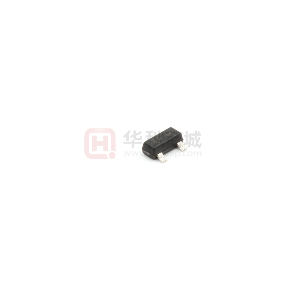
SOT-23
SOT-23 1: Ref;
2: Cathode; 3: Anode
Features:
• Precise Reference Voltage to 1.24V
• Guaranteed 1% Reference Voltage
Tolerance
• Sink Current Capability, 80µA to100mA
• Quick Turn-on
• Adjustable Output Voltage, Vo=VREF to 18V
• 0.2 Ω Typical Output Impedance
• Marking:EA
We declare that the material of product is ROHS
compliant and does not contain any B r, Cl, and
Sb203
Ordering Information
Device
Marking
Shipping
LR432ALT1G
EA
3000/Tape & Reel
LR432ALT3G
EA
10000/Tape & Reel
Ver 1.6
1/7
�LESHAN RADIO COMPANY, LTD.
Absolute Maximum Ratings
Symbol
VKA
IK
I REF
Tj
Topr
Parameter
Cathode voltage
Continuous cathode current range
Reference current range
Operating Junction Temperature Range
Operating Ambient Temperature
Electrical Characteristics
Symbol
TA= 25°C
Reference voltage
VDEV
VREF Temp Deviation
∆VREF/∆VKA
Ratio of Change in VREF to
Change in Cathode Voltage
IREF
Reference Input Current
IREF(DEV)
IREF Temp Deviation
Ik(off)
Off-state cathode current
IK(MIN)
Unit
V
mA
mA
°C
°C
( unless otherwise noted)
Parameter
VREF
Zka
Rating
18
100
3
150
- 40 to 105
Dynamic Output Impedance
Minimum Operating Current
Test Conditions
VKA=VREF, lK=10mA
(Fig. 1)
TA =25°C
TA=full range(see Note1)
VKA=VREF, lK=10mA(Fig. 1)
IK=10mA, VKA=18V to VREF
(Fig. 2)
IK=10mA, R1 =10kΩ R2=∞
(Fig.2)
TK=full range (see Note 1), R1
=10kΩ, R2=∞, IK=10mA (Fig.
2)
VREF=0 V,(Fig.3)
Vk=18V
Vka=Vref, Ik=1mA to 100mA
F ≤1kHz (Fig. 1)
VKA=VREF(Fig. 1)
LR432ALT1G
Min
1.228
Typ
1.240
Unit
Max
1.252
V
10
25
mV
-1
-2.7
mV / V
0.25
0.5
µA
0.05
0.3
µA
0.04
0.5
µA
0.2
0.4
Ω
60
80
µA
�
2/7
�LESHAN RADIO COMPANY, LTD.
Fig.1 Test Circuit for Vka=Vref,
Vo=Vka=Vref, Co=0.1µF
Fig.2 Test Circuit for Vka>Vref,
Vo=Vka=Vref·(1+R1/R2)+Iref·R1,
Co=0.1µF
Fig.3 Test Circuit for Ik(off)
�
3/7
�LESHAN RADIO COMPANY, LTD.
Typical Performance Characteristics
IKA=10mA
TA=25oC
50
Output
IKA
15KΩ
40
+
9µF
30
232Ω
+
-
AV-Small Signal Voltage Amplification (dB)
60
-
8.25KΩ
GND
20
Test Circuit for Voltage Amplification
10
0
10K
1K
100K
f-Frequency-Hz
1M
10M
Fig.4 Small-Signal Voltage Amplification vs Frequency
∣ZKA∣ Reference Impedance (Ω)
100
I KA=10mA
o
TA =25 C
1KΩ
Output
I KA
10
50Ω
+
GND
1
Test Circuit for Reference Impedance
0.1
1K
10K
100K
1M
10M
f-Frequency-Hz
Fig.5 Reference Impedance vs Frequency
150Ω
I KA
CL
+
-
VBATT
Test Circuit for Curve A
I KA
150Ω
R1=10KΩ
CL
R2
+
-
VBATT
Fig.6 STABILITY BOUNDARY CONDITIONS
Test Circuit for Curve B, C, and D
Unstable
region
VKA(V)
R1(KΩ)
R2(KΩ)
A
B
Vref
5.0
0
30
∞
10
4/7
�LESHAN RADIO COMPANY, LTD.
1.253
0.40
VKA=VREF
IKA=10mA
R1=10KΩ
R2=Infinite
IKA=10mA
0.35
Reference Current (μA)
Reference Voltage (V)
1.252
1.251
1.250
1.249
1.248
0.30
0.25
0.20
0.15
1.247
-50
-25
0
25
50
75
100
125
0.10
-50
150
-25
o
Ambient Temperature ( C)
25
50
75
100
o
Ambient Temperature ( C)
Fig 7. Reference Voltage vs. Ambient Temperature
Fig 8. Reference Current vs. Ambient Temperature
400
150
VKA=VREF
100
VKA=VREF
300
o
TA=25 C
o
TA=25 C
Cathode Current (μA)
Cathode Current (mA)
0
50
0
-50
200
100
0
-100
-200
-100
-300
-150
-1
0
1
-1.0
-0.5
0.0
0.5
1.0
1.5
Cathode Voltage (V)
Cathode Voltage (V)
Figu 10. Cathode Current vs. Cathode Voltage
Fig 9. Cathode Current vs. Cathode Voltage
Input and Output Voltage (V)
3
Input
Output
R1
1.8KΩ
2
Pulse
Generator
f=100KHz
1
R2
50Ω
Output
GND
0
-1
0
1
2
3
4
5
6
Time (μS)
Fig 11. Pulse Response of Input and Output Voltage
5/7
�LESHAN RADIO COMPANY, LTD.
Application Examples
VIN
V IN
R CL
R
R1B
R1A
ON
R2A
R2B
I OUT
V IN
+
OFF
LED on when Low Limit < V < High Limit
IN
(1+R1B/R2B)
Low Limit ≈ V
REF
(1+R1A/R2A)
High Limit ≈ V
Delay = RC x ln (
VIN
V -V
IN
)
I OUT = V REF / RCL
REF
REF
Fig. 13 Delay
Timer
Fig. 12 Voltage
Monitor
V IN
I OUT
V IN
Fig. 14 Current Limiter or Current
Source
V OUT
VIN
R1
R1
R2
R2
RS
LIMIT
V OUT = (1 + R1/R2) x VREF
I OUT = V REF / RS
Fig. 15 Constant-Current
Sink
V OUT
PUSE
Fig. 16 Higher-Current Shunt
Regulator
(1 + R1/R2) x VREF
Fig. 17 Crow Bar
VIN
R1A
R1B
+
R2A
Low Limit
High Limit
R2B
Output ON when
Low Limit
很抱歉,暂时无法提供与“LR432ALT1G”相匹配的价格&库存,您可以联系我们找货
免费人工找货- 国内价格
- 10+0.37828
- 100+0.30254
- 600+0.29951
- 1200+0.29352
- 国内价格
- 10+0.41267
- 100+0.33005
- 300+0.28869