LSI1012XT1G
S-LSI1012XT1G
N-Channel 1.8-V (G-S) MOSFET
1. FEATURES
●
Gate-Source ESD Protected
●
High-Side Switching
●
Low On-Resistance: 0.7Ω
●
Low Threshold: 0.8 V (typ)
●
Fast Switching Speed: 10 ns
●
We declare that the material of product compliance with
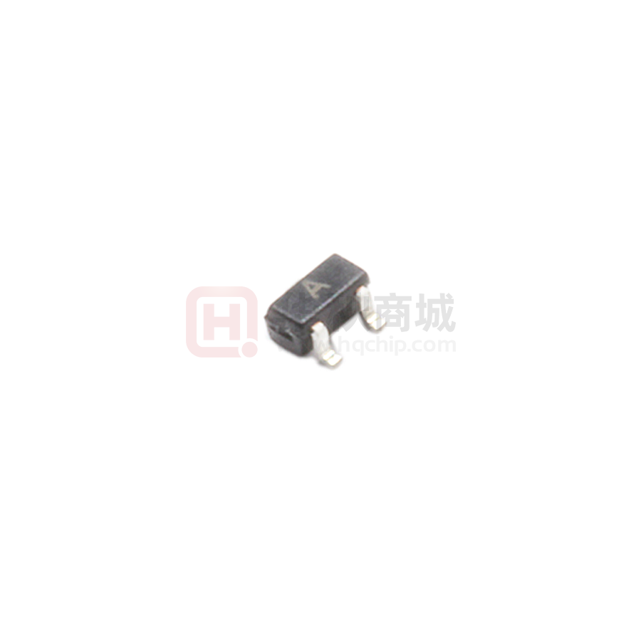
SC89
Gate
RoHS requirements and Halogen Free.
●
1
S- prefix for automotive and other applications requiring
unique site and control change requirements; AEC-Q101
3
Drain
qualified and PPAP capable.
Source
2
2. APPLICATION
●
Drivers: Relays, Solenoids, Lamps, Hammers,Displays, Memories
●
Battery Operated Systems
●
Power Supply Converter Circuits
●
Load/Power Switching Cell Phones, Pagers
(Top View)
MARKING DIAGRAM
3. DEVICE MARKING AND RESISTOR VALUES
A
Device
Marking
Shipping
LSI1012XT1G
A
3000/Tape&Reel
LSI1012XT3G
A
10000/Tape&Reel
1
M
3
2
A = Specific Device Code
M = Month Code
4. MAXIMUM RATINGS(Ta = 25ºC)
Parameter
Symbol
Drain-Source Voltage
VDS
Gate-Source Voltage
Continuous Drain Current (TJ = 150℃)
(Note 2)
TA = 85℃
ID
TA = 25℃
TA = 85℃
Operating Junction and Storage Temperature Range
IS
PD
TJ , Tstg
±6
V
500
400
350
1000
275
250
275
250
160
140
−55 ~+150
Unit
V
600
IDM
Continuous Source Current (diode conduction)(Note 2)
Steady State
20
VGS
TA = 25℃
Pulsed Drain Current(Note 1)
Maximum Power Dissipation(Note 2)
5 secs
mA
mW
℃
1.Pulse test; pulse width ≤300 µs, duty cycle ≤2%.
2.Guaranteed by design, not subject to production testing.
Leshan Radio Company, LTD.
Rev.D Jan. 2021
1/5
�LSI1012XT1G, S-LSI1012XT1G
N-Channel 1.8-V (G-S) MOSFET
5. ELECTRICAL CHARACTERISTICS (Ta= 25ºC)
Static
Characteristic
Drain-Source Breakdown Voltage
(VGS = 0V, ID = 250µA)
Gate Threshold Voltage
(VDS = VGS , ID = 250µA )
Gate-Body Leakage
(VDS = 0 V, VGS = ±4.5 V)
Symbol
Min.
Typ.
Max.
Unit
V(BR)DSS
20
-
-
V
VGS(th)
0.45
-
0.9
V
IGSS
-
±0.5
±1
µA
IDSS
-
0.3
100
nA
-
-
5
µA
-
0.41
0.7
-
0.53
0.85
Ω
-
0.7
1.25
VSD
-
0.8
1.2
Zero Gate Voltage Drain Current
(VDS = 20 V, VGS = 0 V )
(VDS = 20 V, VGS = 0 V, TJ = 85℃)
Drain-Source On-State Resistance(Note 1)
(VGS = 4.5 V, ID = 600 mA)
RDS(on)
(VGS = 2.5 V, ID = 500 mA)
(VGS = 1.8 V, ID = 350 mA)
Diode Forward Voltage(Note 1)
(IS = 150 mA, VGS = 0 V)
V
Dynamic(Note 2)
Total Gate Charge
Gate-Source Charge
Gate-Drain Charge
Turn-On Delay Time
Rise Time
Turn-Off Delay Time
Fall Time
Leshan Radio Company, LTD.
(VDS = 10 V,
VGS = 4.5 V, ID
= 250 mA)
(VDD = 10 V, RL
= 47Ω,ID=200
mA, VGEN = 4.5
V, RG = 10Ω)
Qg
-
750
-
Qgs
-
75
-
Qgd
225
td(on)
-
5
-
tr
-
5
-
td(off)
-
25
-
tf
Rev.D Jan. 2021
11
pC
ns
2/5
�LSI1012XT1G, S-LSI1012XT1G
N-Channel 1.8-V (G-S) MOSFET
6.ELECTRICAL CHARACTERISTICS CURVES
0.5
0.45
0.4
0.4
ID Drain Current(A)
0.45
0.35
ID Drain Current(A)
0.5
VGS=2V,2.5V,3V
VGS=1.5V
0.3
0.25
VGS=1.4V
0.2
0.15
VDS=10V
0.35
25℃
0.3
0.25
0.2
-55℃
0.15
150℃
VGS=1.3V
0.1
0.1
VGS=1.2V
0.05
0.05
0
0
0
1
2
3
4
VDS Drain to Source Voltage(V)
5
0.0
0.5
1.0
1.5
VGS Gate to Source Voltage(V)
ID vs. VGS
ID vs. VDS
1.0
1
0.8
RDS(on) On Resistance (Ω)
IS Diode Forward Current(A)
0.9
0.1
25℃
150℃
-55℃
0.01
VGS=1.8V
0.7
0.6
0.5
VGS=2.5V
0.4
0.3
VGS=4.5V
0.2
0.1
0.0
0.001
0.2
0.4
0.6
0.8
VSD Diode Forward Voltage(V)
1.0
0.2
0.6
RDS(on) vs. ID
IS vs. VSD
Leshan Radio Company, LTD.
0.3
0.4
0.5
ID,Drain Current(A)
Rev.D Jan. 2021
3/5
�LSI1012XT1G, S-LSI1012XT1G
N-Channel 1.8-V (G-S) MOSFET
6.ELECTRICAL CHARACTERISTICS CURVES(Con.)
0.7
1.6
ID=600mA
0.6
RDS(on) On Resistance (Ω)
RDS(on) On Resistance (Ω)
1.4
1.2
25℃
1.0
0.8
150℃
0.6
VGS=2.5V,ID=500mA
0.5
0.4
0.3
VGS=4.5V,ID=600mA
0.2
0.4
0.1
-55℃
0.2
0.0
0.0
1
2
3
4
VGS Gate to Source Voltage(V)
-50
5
-25
0
RDS(on) vs. VGS
25 50 75 100 125 150
Tj Temperature(℃)
RDS(on) vs. Tj
100
1.0
90
ID=250uA
f=1.0MHz
Ta=25℃
Capacitance(pF)
VGSTH Threshold Voltage (V)
80
0.8
0.6
70
Ciss
60
50
40
30
Coss
20
10
Crss
0
0.4
-50
-25
0
25
50
75
Tj Temperature(℃)
100
125
150
0
10
15
20
VDS Drain to Source Voltage(V)
Capacitance
VGSTH vs. Tj
Leshan Radio Company, LTD.
5
Rev.D Jan. 2021
4/5
�LSI1012XT1G, S-LSI1012XT1G
N-Channel 1.8-V (G-S) MOSFET
7.OUTLINE AND DIMENSIONS
Notes:
1. DIMENSIONING AND TOLERANCING PER ANSI
Y14.5M, 1982.
2. CONTROLLING DIMENSION: MILLIMETERS.
3. MAXIMUM LEAD THICKNESS INCLUDES LEAD
FINISH. MINIMUM LEAD THICKNESS IS THE MINIMUM
THICKNESS OF BASE MATERIAL.
4. DIMENSIONS A AND B DO NOT INCLUDE MOLD
FLASH, PROTRUSIONS OR GATE BURRS.
MILLIMETERS
INCHES
DIM MIN
A 1.50
NOM
MAX
MIN
NOM
MAX
1.60
1.70
0.059 0.063 0.067
B
0.75
0.85
0.95
0.030 0.034 0.040
C
0.60
0.70
0.80
0.024 0.028 0.031
D
0.23
0.28
0.33
0.009 0.011 0.013
G
0.50BSC
0.020BSC
H
0.53REF
0.021REF
J
0.10
0.15
0.20
0.004 0.006 0.008
K
0.30
0.40
0.50
0.012 0.016
L
1.10REF
0.02
0.043REF
M
---
---
10°
---
---
10°
N
---
---
10°
---
---
10°
S
1.50
1.60
1.70
0.059 0.063 0.067
8.SOLDERING FOOTPRINT
Leshan Radio Company, LTD.
Rev.D Jan. 2021
5/5
�DISCLAIMER
●
Before you use our Products, you are requested to carefully read this document and fully understand its
contents. LRC shall not be in any way responsible or liable for failure, malfunction or accident arising
from the use of any LRC’s Products against warning, caution or note contained in this document.
●
All information contained in this document is current as of the issuing date and subject to change without
any prior notice. Before purchasing or using LRC's Products,please confirm the latest information with a
LRC sales representative.
�
很抱歉,暂时无法提供与“LSI1012XT1G”相匹配的价格&库存,您可以联系我们找货
免费人工找货- 国内价格
- 20+0.21602
- 400+0.17196
- 1600+0.14751
- 国内价格
- 20+0.23540
- 200+0.18430
- 600+0.15780
- 4000+0.13330
- 8000+0.11960
- 国内价格
- 20+0.23566
- 200+0.18760
- 600+0.16092
- 4000+0.13598
- 8000+0.12204
- 国内价格
- 1+0.46785
- 500+0.15631
- 2500+0.10392