88E1111 Product Brief
Integrated 10/100/1000 Ultra Gigabit Ethernet Transceiver
Doc. No. MV-S105540-00, Rev. -March 4, 2009 Document Classification: Proprietary Information Marvell. Moving Forward Faster
�88E1111 Product Brief Integrated 10/100/1000 Ultra Gigabit Ethernet Transceiver
Document Conventions
Note: Provides related information or information of special importance.
Caution: Indicates potential damage to hardware or software, or loss of data.
Warning: Indicates a risk of personal injury.
Document Status
Advance Information Preliminary Information Final Information This document contains design specifications for initial product development. Specifications may change without notice. Contact Marvell Field Application Engineers for more information. This document contains preliminary data, and a revision of this document will be published at a later date. Specifications may change without notice. Contact Marvell Field Application Engineers for more information. This document contains specifications on a product that is in final release. Specifications may change without notice. Contact Marvell Field Application Engineers for more information.
Technical Publications: 1.00
Doc Status: Advance
For more information, visit our website at: www.marvell.com
Disclaimer No part of this document may be reproduced or transmitted in any form or by any means, electronic or mechanical, including photocopying and recording, for any purpose, without the express written permission of Marvell. Marvell retains the right to make changes to this document at any time, without notice. Marvell makes no warranty of any kind, expressed or implied, with regard to any information contained in this document, including, but not limited to, the implied warranties of merchantability or fitness for any particular purpose. Further, Marvell does not warrant the accuracy or completeness of the information, text, graphics, or other items contained within this document. Marvell products are not designed for use in life-support equipment or applications that would cause a life-threatening situation if any such products failed. Do not use Marvell products in these types of equipment or applications. With respect to the products described herein, the user or recipient, in the absence of appropriate U.S. government authorization, agrees: 1) Not to re-export or release any such information consisting of technology, software or source code controlled for national security reasons by the U.S. Export Control Regulations ("EAR"), to a national of EAR Country Groups D:1 or E:2; 2) Not to export the direct product of such technology or such software, to EAR Country Groups D:1 or E:2, if such technology or software and direct products thereof are controlled for national security reasons by the EAR; and, 3) In the case of technology controlled for national security reasons under the EAR where the direct product of the technology is a complete plant or component of a plant, not to export to EAR Country Groups D:1 or E:2 the direct product of the plant or major component thereof, if such direct product is controlled for national security reasons by the EAR, or is subject to controls under the U.S. Munitions List ("USML"). At all times hereunder, the recipient of any such information agrees that they shall be deemed to have manually signed this document in connection with their receipt of any such information. Copyright © 2009. Marvell International Ltd. All rights reserved. Marvell, the Marvell logo, Moving Forward Faster, Alaska, Fastwriter, Datacom Systems on Silicon, Libertas, Link Street, NetGX, PHYAdvantage, Prestera, Raising The Technology Bar, The Technology Within, Virtual Cable Tester, and Yukon are registered trademarks of Marvell. Ants, AnyVoltage, Discovery, DSP Switcher, Feroceon, GalNet, GalTis, Horizon, Marvell Makes It All Possible, RADLAN, UniMAC, and VCT are trademarks of Marvell. All other trademarks are the property of their respective owners.
Doc. No. MV-S105540-00 Rev. -Page 2 Document Classification: Proprietary Information
Copyright © 2009 Marvell March 4, 2009, Advance
�88E1111 Product Brief Integrated 10/100/1000 Ultra Gigabit Ethernet Transceiver
O VERVIEW
The Alaska® Ultra 88E1111 Gigabit Ethernet Transceiver is a physical layer device for Ethernet 1000BASE-T, 100BASE-TX, and 10BASE-T applications. It is manufactured using standard digital CMOS process and contains all the active circuitry required to implement the physical layer functions to transmit and receive data on standard CAT 5 unshielded twisted pair. The 88E1111 device incorporates the Marvell Virtual Cable Tester® (VCT™) feature, which uses Time Domain Reflectometry (TDR) technology for the remote identification of potential cable malfunctions, thus reducing equipment returns and service calls. Using VCT, the Alaska 88E1111 device detects and reports potential cabling issues such as pair swaps, pair polarity and excessive pair skew. The device will also detect cable opens, shorts or any impedance mismatch in the cable and report accurately within one meter the distance to the fault. The 88E1111 device supports the Gigabit Media Independent Interface (GMII), Reduced GMII (RGMII), Serial Gigabit Media Independent Interface (SGMII), the Ten-Bit Interface (TBI), and Reduced TBI (RTBI) for direct connection to a MAC/Switch port. The 88E1111 device incorporates an optional 1.25 GHz SERDES (Serializer/Deserializer). The serial interface may be connected directly to a fiber-optic transceiver for 1000BASE-T/1000BASE-X media conversion applications. Additionally, the 88E1111 device may be used to implement 1000BASE-T Gigabit Interface Converter (GBIC) or Small Form Factor Pluggable (SFP) modules. The 88E1111 device uses advanced mixed-signal processing to perform equalization, echo and crosstalk cancellation, data recovery, and error correction at a gigabit per second data rate. The device achieves robust performance in noisy environments with very low power dissipation. The 88E1111 device is offered in three different package options including a 117-Pin TFBGA, a 96-pin BCC featuring a body size of only 9 x 9 mm, and a 128 PQFP package.
F EATURES
• •
10/100/1000BASE-T IEEE 802.3 compliant Supports GMII, TBI, reduced pin count GMII (RGMII), reduced pin count TBI (RTBI), and serial GMII (SGMII) interfaces Integrated 1.25 GHz SERDES for 1000BASE-X fiber applications Four RGMII timing modes Energy Detect and Energy Detect+ low power modes Three loopback modes for diagnostics “Downshift” mode for two-pair cable installations Fully integrated digital adaptive equalizers, echo cancellers, and crosstalk cancellers Advanced digital baseline wander correction Automatic MDI/MDIX crossover at all speeds of operation Automatic polarity correction IEEE 802.3u compliant Auto-Negotiation Software programmable LED modes including LED testing Automatic detection of fiber or copper operation Supports IEEE 1149.1 JTAG Two-Wire Serial Interface (TWSI) and MDC/MDIO CRC checker, packet counter Packet generation Virtual Cable Tester (VCT) Auto-Calibration for MAC Interface outputs Requires only two supplies: 2.5V and 1.0V (with 1.2V option for the 1.0V supply) I/Os are 3.3V tolerant Low power dissipation Pave = 0.75W 117-Pin TFBGA, 96-Pin BCC, and 128 PQFP package options 117-Pin TFBGA and 96-Pin BCC packages available in Commercial or Industrial grade RoHS 6/6 compliant packages available
• • • • • • • • • • • • • • • • • • • • • • • •
Copyright © 2009 Marvell March 4, 2009, Advance Document Classification: Proprietary Information
Doc. No. MV-S105540-00, Rev. -Page 3
�88E1111 Product Brief Integrated 10/100/1000 Ultra Gigabit Ethernet Transceiver
10/100/1000 Mbps Ethernet MAC MAC Interface Options - GMII/MII - TBI - RGMII - RTBI - SGMII - Serial Interface
88E1111 Device
M a g n e t i c s
RJ-45
Media Types: - 10BASE-T - 100BASE-TX - 1000BASE-T
88E1111 Device used in Copper Application
10/100/1000 Mbps Ethernet MAC MAC Interface Options - GMII/MII - RGMII
88E1111 Device
Serial Interface
Fiber Optics
Media Types: - 1000BASE-X
88E1111 Device used in Fiber Application
(Effective SGMII MAC) Gigabit Ethernet MAC MAC Interface Options - GMII - RGMII
88E1111 Device
Serial Interface - 4-pin SGMIII
3-Speed SFP
88E1111 RGMII/GMII MAC to SGMII MAC Conversion
Doc. No. MV-S105540-00, Rev. -Page 4 Document Classification: Proprietary Information Copyright © 2009 Marvell March 4, 2009, Advance
�Table of Contents
1.1 1.2 1.3 1.4 1.5 1.6 1.7 1.8 2.1 2.2 2.3 2.4 3.1 117-Pin TFBGA Package................................................................................................6 96-Pin BCC Package .....................................................................................................7 128-Pin PQFP Package ..................................................................................................8 Pin Description ...............................................................................................................9
1.4.1 Pin Type Definitions............................................................................................................ 9
I/O State at Various Test or Reset Modes ..................................................................33 117-Pin TFBGA Pin Assignment List - Alphabetical by Signal Name .....................34 96-Pin BCC Pin Assignment List - Alphabetical by Signal Name............................36 128-Pin PQFP Pin Assignment List - Alphabetical by Signal Name........................38 117-pin TFBGA Package..............................................................................................40 96-pin BCC Package - Top View .................................................................................42 96-Pin BCC Package - Bottom View ...........................................................................43 128-Pin PQFP Package ................................................................................................44 Ordering Part Numbers and Package Markings........................................................45
3.1.1 3.1.2 RoHS 5/6 Compliant Marking Examples .......................................................................... 46 RoHS 6/6 Compliant Marking Examples .......................................................................... 49
Copyright © 2009 Marvell March 4, 2009, Advance Document Classification: Proprietary Information
Doc. No. MV-S105540-00, Rev. -Page 5
�88E1111 Product Brief Integrated 10/100/1000 Ultra Gigabit Ethernet Transceiver
Section 1. Signal Description
The 88E1111 device is a 10/100/1000BASE-T/1000BASE-X Gigabit Ethernet transceiver.
1.1 117-Pin TFBGA Package
Figure 1: 88E1111 Device 117-Pin TFBGA Package (Top View)
1 2 3 4 5 6 7 8 9 LED_ LINK1000 VDDOH
A
RXD5
RXD6
S_IN+
S_IN-
S_CLK+
S_CLK-
S_OUT+
S_OUTLED_ LINK100 LED_ LINK10 CONFIG[0] LED_ DUPLEX CONFIG[2]
A
B
RX_DV
RXD0
RXD3
VDDO
CRS
COL
AVDD
B
C
RX_CLK
VDDO
RXD2
RXD4
RXD7
DVDD
DVDD
LED_RX
C
D
TX_CLK
RX_ER
RXD1
VSS
VSS
VSS
DVDD
LED_TX
D
E
TX_EN
GTX_CLK
DVDD
VSS
VSS
VSS
DVDD
CONFIG[1]
E
F
TXD0
TX_ER
DVDD
VSS
VSS
VSS
VDDOH
CONFIG[4]
F
G
NC
TXD1
TXD2
VSS
VSS
VSS
CONFIG[3]
CONFIG[6] SEL_ FREQ VDDOH
CONFIG[5]
G
H
TXD4
TXD3
TXD5
VSS
VSS
VSS
VSSC
XTAL1
H
J
TXD6
TXD7
DVDD
VSS
VSS
VSS
DVDD
XTAL2
J
K
VDDO
125CLK
RESETn
VSS
VSS
VSS
NC
TDO
VDDOX
K
L
INTn
VDDOX
MDC
COMA
VSS
VSS
TDI
TMS
TCK
L
M
MDIO
RSET
AVDD
AVDD
HSDAC+
HSDAC-
AVDD
AVDD
TRSTn
M
N
MDI[0]+
MDI[0]-
MDI[1]+
MDI[1]-
AVDD
MDI[2]+
MDI[2]-
MDI[3]+
MDI[3]-
N
1
2
3
4
5
6
7
8
9
Figure 2: Pin A1 Location
Pin A1 location
88E1111-BAB
Doc. No. MV-S105540-00, Rev. -Page 6 Document Classification: Proprietary Information
Copyright © 2009 Marvell March 4, 2009, Advance
�Signal Description
96-Pin BCC Package
1.2
96-Pin BCC Package
Figure 3: 88E1111 Device 96-Pin BCC Package (Top View)
73 71 69 67 65 63 61 59 57 55 53 51 50
TDO
CONFIG[0]
CONFIG[2]
CONFIG[3]
CONFIG[5]
LED_LINK 1000
LED_RX
XTAL1
DVDD
DVDD
DVDD
VSSC
72
70
68
66
64
62
60
58
56
54
LED_DUPL EX
52
NC
CONFIG[1]
CONFIG[4]
LED_TX
VDDOH
VDDOH
VDDOH
XTAL2
DVDD
SEL_ FREQ
74 75
LED_LINK 100
CONFIG[6]
TCK VDDOX
49
48
TRSTn
S_OUT-
47
76 77
S_OUT+
LED_LINK 10
0
VSS
TMS
46
AVDD
45
78 79
S_CLK+
AVDD
TDI
44
MDI[3]-
43
80 81
S_IN-
S_CLK-
MDI[3]+
42
MDI[2]-
41
82 83
COL
S_IN+
AVDD
40
MDI[2]+
39
84 85
DVDD
CRS
HSDAC-
38
HSDAC+
86 87
RXD6
RXD7
88E1111 - CAA
37
AVDD
36
AVDD
35
88 89
RXD5
VDDO
MDI[1]-
34
MDI[1]+
33
90 91
RXD3
RXD4
AVDD
32
MDI[0]-
31
92 93
RXD2
RXD1
RSET
30
MDI[0]+
29
94 95 96
RXD0
RX_DV
RESETn
28
COMA
27
GTX_CLK
RX_CLK
TX_CLK
125CLK
DVDD
DVDD
TXD1
TXD2
TXD3
TXD5
TXD7
VDDOX
26
MDC
VDDO
25
2
4
6
8
10
12
14
16
18
20
RX_ER
TX_ER
TX_EN
VDDO
VDDO
DVDD
DVDD
22
11
1
3
5
7
9
13
15
17
19
21
23
Copyright © 2009 Marvell March 4, 2009, Advance Document Classification: Proprietary Information
Doc. No. MV-S105540-00, Rev. -Page 7
24
MDIO
TXD0
TXD4
TXD6
INTn
NC
�88E1111 Product Brief Integrated 10/100/1000 Ultra Gigabit Ethernet Transceiver
1.3 128-Pin PQFP Package
Figure 4: 88E1111 Device 128-Pin PQFP Package (Top View)
VSS VSS LED_LINK10 LED_LINK100 LED_LINK1000 VDDOH DVDD LED_DUPLEX VSS VSS LED_RX LED_TX DVDD VDDOH CONFIG[0] CONFIG[1] CONFIG[2] DVDD VSS VSS CONFIG[3] CONFIG[4] CONFIG[5] CONFIG[6] DVDD SEL_FREQ XTAL1 XTAL2 VSSC VDDOH TDO VDDOX TCK TMS TRSTn TDI VSS VSS 103 104 105 106 107 108 109 110 111 112 113 114 115 116 117 118 119 120 121 122 123 124 125 126 127 128 102 101 100 99 98 97 96 95 94 93 92 91 90 89 88 87 86 85 84 83 82 81 80 79 78 77 76 75 74 73 72 71 70 69 68 67 66 65
VSS AVDD S_OUTVSS S_OUT+ VSS S_CLKS_CLK+ VSS S_INS_IN+ COL CRS VSS DVDD DVDD VSS RXD7 RXD6 VDDO RXD5 RXD4 RXD3 RXD2 VSS RXD1
88E1111 - RCJ
Top View
64 63 62 61 60 59 58 57 56 55 54 53 52 51 50 49 48 47 46 45 44 43 42 41 40 39
AVDD VSS MDI[3]MDI[3]+ VSS AVDD VSS MDI[2]MDI[2]+ VSS HSDACHSDAC+ AVDD VSS NC AVDD VSS MDI[1]MDI[1]+ VSS AVDD VSS MDI[0]MDI[0]+ VSS RSET
Doc. No. MV-S105540-00, Rev. -Page 8 Document Classification: Proprietary Information
VSS DVDD RXD0 RX_DV VDDO DVDD RX_CLK RX_ER VSS TX_CLK VDDO DVDD TX_ER GTX_CLK VSS TX_EN DVDD TXD0 TXD1 TXD2 VSS VSS DVDD TXD3 TXD4 TXD5 DVDD TXD6 TXD7 VDDO 125CLK INTn MDIO VDDOX MDC RESETn COMA VSS
1 2 3 4 5 6 7 8 9 10 11 12 13 14 15 16 17 18 19 20 21 22 23 24 25 26 27 28 29 30 31 32 33 34 35 36 37 38
Copyright © 2009 Marvell March 4, 2009, Advance
�Signal Description
Pin Description
1.4 Pin Description
1.4.1 Pin Type Definitions
Pi n Type
H I/O I O PU PD D Z mA
D efin i ti o n
Input with hysteresis Input and output Input only Output only Internal pull up Internal pull down Open drain output Tri-state output DC sink capability
Copyright © 2009 Marvell March 4, 2009, Advance Document Classification: Proprietary Information
Doc. No. MV-S105540-00, Rev. -Page 9
�88E1111 Product Brief Integrated 10/100/1000 Ultra Gigabit Ethernet Transceiver
Table 1:
Media Dependent Interface 128 -PQF P Pi n Na me Pin #
41 42 MDI[0]+ MDI[0]-
117-TFBGA 9 6-BCC Pin # Pin #
N1 N2 29 31
Pi n Ty pe
I/O, D
Des cription
Media Dependent Interface[0]. In 1000BASE-T mode in MDI configuration, MDI[0]± correspond to BI_DA±. In MDIX configuration, MDI[0]± correspond to BI_DB±. In 100BASE-TX and 10BASE-T modes in MDI configuration, MDI[0]± are used for the transmit pair. In MDIX configuration, MDI[0]± are used for the receive pair. MDI[0]± should be tied to ground if not used.
N3 N4
33 34
46 47
MDI[1]+ MDI[1]-
I/O, D
Media Dependent Interface[1]. In 1000BASE-T mode in MDI configuration, MDI[1]± correspond to BI_DB±. In MDIX configuration, MDI[1]± correspond to BI_DA±. In 100BASE-TX and 10BASE-T modes in MDI configuration, MDI[1]± are used for the receive pair. In MDIX configuration, MDI[1]± are used for the transmit pair. MDI[1]± should be tied to ground if not used.
Doc. No. MV-S105540-00, Rev. -Page 10 Document Classification: Proprietary Information
Copyright © 2009 Marvell March 4, 2009, Advance
�Signal Description
Pin Description
Table 1:
Media Dependent Interface (Continued) 12 8-PQF P Pin Name Pin #
56 57 MDI[2]+ MDI[2]-
117-T FB GA 9 6-BCC Pin # Pin #
N6 N7 39 41
Pin Type
I/O, D
Des cription
Media Dependent Interface[2]. In 1000BASE-T mode in MDI configuration, MDI[2]± correspond to BI_DC±. In MDIX configuration, MDI[2]± corresponds to BI_DD±. In 100BASE-TX and 10BASE-T modes, MDI[2]± are not used. MDI[2]± should be tied to ground if not used.
N8 N9
42 43
61 62
MDI[3]+ MDI[3]-
I/O, D
Media Dependent Interface[3]. In 1000BASE-T mode in MDI configuration, MDI[3]± correspond to BI_DD±. In MDIX configuration, MDI[3]± correspond to BI_DC±. In 100BASE-TX and 10BASE-T modes, MDI[3]± are not used. MDI[3]± should be tied to ground if not used.
Copyright © 2009 Marvell March 4, 2009, Advance Document Classification: Proprietary Information
Doc. No. MV-S105540-00, Rev. -Page 11
�88E1111 Product Brief Integrated 10/100/1000 Ultra Gigabit Ethernet Transceiver
The GMII interface supports both 1000BASE-T and 1000BASE-X modes of operation. The GMII interface pins are also used for the TBI interface. See Table 3 for TBI pin definitions. The MAC interface pins are 3.3V tolerant. Table 2: GMII/MII Interfaces 128 -PQF P Pin Name Pin #
14 GTX_CLK
117-T FBGA 96 -BCC Pi n # Pin #
E2 8
Pin Typ e
I
Desc ription
GMII Transmit Clock. GTX_CLK provides a 125 MHz clock reference for TX_EN, TX_ER, and TXD[7:0]. This clock can be stopped when the device is in 10/100BASET modes, and also during Auto-Negotiation. MII Transmit Clock. TX_CLK provides a 25 MHz clock reference for TX_EN, TX_ER, and TXD[3:0] in 100BASE-TX mode, and a 2.5 MHz clock reference in 10BASE-T mode. TX_CLK provides a 25 MHz, 2.5 MHz, or 0 MHz clock during 1000 Mbps Good Link, Auto-Negotiation, and Link Lost states depending on the setting of register 20.6:4. The 2.5 MHz clock is the default rate, which may be programmed to another frequency by writing to register 20.6:4.
D1
4
10
TX_CLK
O, Z
E1
9
16
TX_EN
I
GMII and MII Transmit Enable. In GMII/MII mode when TX_EN is asserted, data on TXD[7:0] along with TX_ER is encoded and transmitted onto the cable. TX_EN is synchronous to GTX_CLK, and synchronous to TX_CLK in 100BASE-TX and 10BASE-T modes.
F2
7
13
TX_ER
I
GMII and MII Transmit Error. In GMII/MII mode when TX_ER and TX_EN are both asserted, the transmit error symbol is transmitted onto the cable. When TX_ER is asserted with TX_EN de-asserted, carrier extension symbol is transmitted onto the cable. TX_ER is synchronous to GTX_CLK, and synchronous to TX_CLK in 100BASE-TX and 10BASE-T modes.
Doc. No. MV-S105540-00, Rev. -Page 12 Document Classification: Proprietary Information
Copyright © 2009 Marvell March 4, 2009, Advance
�Signal Description
Pin Description
Table 2:
GMII/MII Interfaces (Continued) 12 8-PQF P Pin Name Pin #
29 28 26 25 24 20 19 18 TXD[7] TXD[6] TXD[5] TXD[4] TXD[3]/TXD[3] TXD[2]/TXD[2] TXD[1]/TXD[1] TXD[0]/TXD[0]
117-T FBGA 9 6-BCC Pin # Pin #
J2 J1 H3 H1 H2 G3 G2 F1 20 19 18 17 16 14 12 11
Pin Ty pe
I
Des cription
GMII and MII Transmit Data. In GMII mode, TXD[7:0] present the data byte to be transmitted onto the cable in 1000BASE-T mode. In MII mode, TXD[3:0] present the data nibble to be transmitted onto the cable in 100BASE-TX and 10BASE-T modes. TXD[7:4] are ignored in these modes, but should be driven either high or low. These pins must not float. TXD[7:0] are synchronous to GTX_CLK, and synchronous to TX_CLK in 100BASE-TX and 10BASE-T modes. Inputs TXD[7:4] should be tied low if not used (e.g., RGMII mode).
C1
2
7
RX_CLK
O, Z
GMII and MII Receive Clock. RX_CLK provides a 125 MHz clock reference for RX_DV, RX_ER, and RXD[7:0] in 1000BASE-T mode, a 25 MHz clock reference in 100BASE-TX mode, and a 2.5 MHz clock reference in 10BASE-T mode. TX_TCLK comes from the RX_CLK pins used in jitter testing. Refer to Register 9 for jitter test modes.
B1
94
4
RX_DV
O, Z
GMII and MII Receive Data Valid. When RX_DV is asserted, data received on the cable is decoded and presented on RXD[7:0] and RX_ER. RX_DV is synchronous to RX_CLK.
D2
3
8
RX_ER
O, Z
GMII and MII Receive Error. When RX_ER and RX_DV are both asserted, the signals indicate an error symbol is detected on the cable. When RX_ER is asserted with RX_DV deasserted, a false carrier or carrier extension symbol is detected on the cable. RX_ER is synchronous to RX_CLK.
Copyright © 2009 Marvell March 4, 2009, Advance Document Classification: Proprietary Information
Doc. No. MV-S105540-00, Rev. -Page 13
�88E1111 Product Brief Integrated 10/100/1000 Ultra Gigabit Ethernet Transceiver
Table 2:
GMII/MII Interfaces (Continued) 128 -PQF P Pin Name Pin #
120 121 123 124 125 126 128 3 115 RXD[7] RXD[6] RXD[5] RXD[4] RXD[3]/RXD[3] RXD[2]/RXD[2] RXD[1]/RXD[1] RXD[0]/RXD[0] CRS
117-T FBGA 96 -BCC Pi n # Pin #
C5 A2 A1 C4 B3 C3 D3 B2 B5 86 87 89 90 91 93 92 95 84
Pin Typ e
O, Z
Desc ription
GMII and MII Receive Data. Symbols received on the cable are decoded and presented on RXD[7:0] in 1000BASE-T mode. In MII mode, RXD[3:0] are used in 100BASE-TX and 10BASE-T modes. In MII mode, RXD[7:4] are driven low. RXD[7:0] is synchronous to RX_CLK.
O, Z
GMII and MII Carrier Sense. CRS asserts when the receive medium is non-idle. In halfduplex mode, CRS is also asserted during transmission. CRS assertion during halfduplex transmit can be disabled by programming register 16.11 to 0. CRS is asynchronous to RX_CLK, GTX_CLK, and TX_CLK.
B6
83
114
COL
O, Z
GMII and MII Collision. In 10/100/ 1000BASE-T full-duplex modes, COL is always low. In 10/100/1000BASE-T halfduplex modes, COL asserts only when both the transmit and receive media are non-idle. In 10BASE-T half-duplex mode, COL is asserted to indicate signal quality error (SQE). SQE can be disabled by clearing register 16.2 to zero. COL is asynchronous to RX_CLK, GTX_CLK, and TX_CLK.
Doc. No. MV-S105540-00, Rev. -Page 14 Document Classification: Proprietary Information
Copyright © 2009 Marvell March 4, 2009, Advance
�Signal Description
Pin Description
The TBI interface supports 1000BASE-T mode of operation. The TBI interface uses the same pins as the GMII interface. The MAC interface pins are 3.3V tolerant. Table 3: TBI Interface 128 -PQFP Pin Name Pin #
14 GTX_CLK/ TBI_TXCLK
117-T FBGA 96 -BCC Pin # Pin #
E2 8
Pin Ty pe
I
Des cription
TBI Transmit Clock. In TBI mode, GTX_CLK is used as TBI_TXCLK. TBI_TXCLK is a 125 MHz transmit clock. TBI_TXCLK provides a 125 MHz clock reference for TX_EN, TX_ER, and TXD[7:0].
D1
4
10
TX_CLK/RCLK1 O, Z
TBI 62.5 MHz Receive Clock- even code group. In TBI mode, TX_CLK is used as RCLK1. TBI Transmit Data. TXD[7:0] presents the data byte to be transmitted onto the cable. TXD[9:0] are synchronous to GTX_CLK. Inputs TXD[7:4] should be tied low if not used (e.g., RTBI mode).
J2 J1 H3 H1 H2 G3 G2 F1 E1
20 19 18 17 16 14 12 11 9
29 28 26 25 24 20 19 18 16
TXD[7] TXD[6] TXD[5] TXD[4] TXD[3] TXD[2] TXD[1] TXD[0] TX_EN/ TXD8
I
I
TBI Transmit Data. In TBI mode, TX_EN is used as TXD8. TXD[9:0] are synchronous to GTX_CLK.
F2
7
13
TX_ER/ TXD9
I
TBI Transmit Data. In TBI mode, TX_ER is used as TXD9. TXD[9:0] are synchronous to GTX_CLK. TX_ER should be tied low if not used (e.g., RTBI mode).
C1
2
7
RX_CLK/ RCLK0 RXD[7] RXD[6] RXD[5] RXD[4] RXD[3] RXD[2] RXD[1] RXD[0] RX_DV/ RXD8
O, Z
TBI 62.5 MHz Receive Clock- odd code group. In the TBI mode, RX_CLK is used as RCLK0. TBI Receive Data code group [7:0]. In the TBI mode, RXD[7:0] present the data byte to be transmitted to the MAC. Symbols received on the cable are decoded and presented on RXD[7:0]. RXD[7:0] are synchronous to RCLK0 and RCLK1.
C5 A2 A1 C4 B3 C3 D3 B2 B1
86 87 89 90 91 93 92 95 94
120 121 123 124 125 126 128 3 4
O, Z
O, Z
TBI Receive Data code group bit 8. In the TBI mode, RX_DV is used as RXD8. RXD[9:0] are synchronous to RCLK0 and RCLK1.
Copyright © 2009 Marvell March 4, 2009, Advance Document Classification: Proprietary Information
Doc. No. MV-S105540-00, Rev. -Page 15
�88E1111 Product Brief Integrated 10/100/1000 Ultra Gigabit Ethernet Transceiver
Table 3:
TBI Interface (Continued) 128 -PQF P Pin Name Pin #
8 RX_ER/ RXD9
117-T FBGA 96 -BCC Pi n # Pin #
D2 3
Pin Ty pe
O, Z
Des cription
TBI Receive Data code group bit 9. In the TBI mode, RX_ER is used as RXD9. RXD[9:0] are synchronous to RCLK0 and RCLK1.
B5 B6
84 83
115 114
CRS/ COMMA COL/LPBK
O, Z I
TBI Valid Comma Detect. In the TBI mode, CRS is used as COMMA. TBI Mode Loopback. In the TBI mode, COL is used to indicate loopback on the TBI. When a “0 - 1" transition is sampled on this pin, bit 0.14 is set to 1. When a “1 - 0" is sampled on this pin, bit 0.14 is reset to 0. If this feature is not used, the COL pin should be driven low on the board. This pin should not be left floating in TBI mode.
Doc. No. MV-S105540-00, Rev. -Page 16 Document Classification: Proprietary Information
Copyright © 2009 Marvell March 4, 2009, Advance
�Signal Description
Pin Description
The RGMII interface supports 10/100/1000BASE-T and 1000BASE-X modes of operation.The RGMII interface pins are also used for the RTBI interface. See Table 5 for RTBI pin definitions. The MAC interface pins are 3.3V tolerant. Table 4: RGMII Interface 12 8-PQF P Pin Name Pin #
14 GTX_CLK/ TXC
117-TFBGA 9 6-BCC Pin # Pin #
E2 8
Pin Type
I
De scrip tio n
RGMII Transmit Clock provides a 125 MHz, 25 MHz, or 2.5 MHz reference clock with ± 50 ppm tolerance depending on speed. In RGMII mode, GTX_CLK is used as TXC. RGMII Transmit Data. In RGMII mode, TXD[3:0] are used as TD[3:0]. In RGMII mode, TXD[3:0] run at double data rate with bits [3:0] presented on the rising edge of GTX_CLK, and bits [7:4] presented on the falling edge of GTX_CLK. In this mode, TXD[7:4] are ignored. In RGMII 10/100BASE-T modes, the transmit data nibble is presented on TXD[3:0] on the rising edge of GTX_CLK.
H2 G3 G2 F1
16 14 12 11
24 20 19 18
TXD[3]/TD[3] TXD[2]/TD[2] TXD[1]/TD[1] TXD[0]/TD[0]
I
E1
9
16
TX_EN/ TX_CTL
I
RGMII Transmit Control. In RGMII mode, TX_EN is used as TX_CTL. TX_EN is presented on the rising edge of GTX_CLK. A logical derivative of TX_EN and TX_ER is presented on the falling edge of GTX_CLK.
C1
2
7
RX_CLK/ RXC
O, Z
RGMII Receive Clock provides a 125 MHz, 25 MHz, or 2.5 MHz reference clock with ± 50 ppm tolerance derived from the received data stream depending on speed. In RGMII mode, RX_CLK is used as RXC. RGMII Receive Control. In RGMII mode, RX_DV is used as RX_CTL. RX_DV is presented on the rising edge of RX_CLK. A logical derivative of RX_DV and RX_ER is presented on the falling edge of RX_CLK.
B1
94
4
RX_DV/ RX_CTL
O, Z
B3 C3 D3 B2
91 93 92 95
125 126 128 3
RXD[3]/RD[3] RXD[2]/RD[2] RXD[1]/RD[1] RXD[0]/RD[0]
O, Z
RGMII Receive Data. In RGMII mode, RXD[3:0] are used as RD[3:0]. In RGMII mode, RXD[3:0] run at double data rate with bits [3:0] presented on the rising edge of RX_CLK, and bits [7:4] presented on the falling edge of RX_CLK. In this mode, RXD[7:4] are ignored. In RGMII 10/100BASE-T modes, the receive data nibble is presented on RXD[3:0] on the rising edge of RX_CLK. RXD[3:0] are synchronous to RX_CLK.
Copyright © 2009 Marvell March 4, 2009, Advance Document Classification: Proprietary Information
Doc. No. MV-S105540-00, Rev. -Page 17
�88E1111 Product Brief Integrated 10/100/1000 Ultra Gigabit Ethernet Transceiver
The RTBI interface supports 1000BASE-T mode of operation. The RTBI interface uses the same pins as the RGMII interface. The MAC interface pins are 3.3V tolerant. Table 5: RTBI Interface 128 -PQF P P i n N a m e Pin #
14 GTX_CLK/ TXC TXD[3]/TD[3] TXD[2]/TD[2] TXD[1]/TD[1] TXD[0]/TD[0]
117-TFBGA 96 -BCC Pi n # Pin #
E2 8
Pin Ty pe
I
Des cription
RGMII Transmit Clock provides a 125 MHz reference clock with ± 50 ppm tolerance. In RTBI mode, GTX_CLK is used as TXC. RTBI Transmit Data. In RTBI mode, TXD[3:0] are used as TD[3:0]. TD[3:0] run at double data rate with bits [3:0] presented on the rising edge of GTX_CLK, and bits [8:5] presented on the falling edge of GTX_CLK. In this mode, TXD[7:4] are ignored. RTBI Transmit Data. In RTBI mode, TX_EN is used as TD4_TD9. TD4_TD9 runs at a double data rate with bit 4 presented on the rising edge of GTX_CLK, and bit 9 presented on the falling edge of GTX_CLK. RTBI Receive Clock provides a 125 MHz reference clock with ± 50 ppm tolerance derived from the received data stream. In RTBI mode, RX_CLK is used as RXC. RTBI Receive Data. In RTBI mode, RXD[3:0] are used as RD[3:0]. RD[3:0] runs at double data rate with bits [3:0] presented on the rising edge of RX_CLK, and bits [8:5] presented on the falling edge of RX_CLK. In this mode, RXD[7:4] are ignored. RTBI Receive Data. In RTBI mode, RX_DV is used as RD4_RD9. RD4_RD9 runs at a double data rate with bit 4 presented on the rising edge of RX_CLK, and bit 9 presented on the falling edge of RX_CLK.
H2 G3 G2 F1
16 14 12 11
24 20 19 18
I
E1
9
16
TX_EN/ TD4_TD9
I
C1
2
7
RX_CLK/ RXC
O, Z
B3 C3 D3 B2
91 93 92 95
125 126 128 3
RXD[3]/RD[3] RXD[2]/RD[2] RXD[1]/RD[1] RXD[0]/RD[0]
O, Z
B1
94
4
RX_DV/ RD4_RD9
O, Z
Doc. No. MV-S105540-00, Rev. -Page 18 Document Classification: Proprietary Information
Copyright © 2009 Marvell March 4, 2009, Advance
�Signal Description
Pin Description
Table 6:
SGMII Interface 12 8-PQF P Pin Name Pin #
113 112 S_IN+ S_IN-
117-T FBGA 9 6-BCC Pin # Pin #
A3 A4 82 81
Pin Type
I
De scrip tio n
SGMII Transmit Data. 1.25 GBaud input Positive and Negative. Input impedance on the S_IN± pins may be programmed for 50 ohm or 75 ohm impedance by setting register 26.6. The input impedance default setting is determined by the 75/50 OHM configuration pin.
A5 A6
79 80
110 109
S_CLK+ S_CLK-
I/O
SGMII 625 MHz Receive Clock. For Serial Interface modes (HWCFG_MODE[3:0] = 1x00) the S_CLK± pins become Signal Detect± (SD±) inputs.
A7 A8
77 75
107 105
S_OUT+ S_OUT-
O, Z
SGMII Receive Data. 1.25 GBaud output Positive and Negative. Output impedance on the S_OUT± pins may be programmed for 50 ohm or 75 ohm impedance by setting register 26.5. Output amplitude can be adjusted via register 26.2:0. The output impedance default setting is determined by the 75/50 OHM configuration pin.
Copyright © 2009 Marvell March 4, 2009, Advance Document Classification: Proprietary Information
Doc. No. MV-S105540-00, Rev. -Page 19
�88E1111 Product Brief Integrated 10/100/1000 Ultra Gigabit Ethernet Transceiver
Table 7:
1.25 GHz Serial High Speed Interface 128 -PQF P P i n N a m e Pin #
113 112 S_IN+ S_IN-
117-T FBGA 96 -BCC Pi n # Pin #
A3 A4 82 81
Pin Ty pe
I
Des cription
1.25 GHz input - Positive and Negative. When this interface is used as a MAC interface, the MAC transmitter’s positive output connects to the S_IN+. The MAC transmitter’s negative output connects to the S_IN-. When this interface is used as a fiber interface, the fiber-optic transceiver’s positive output connects to the S_IN+. The fiber-optic transceiver’s negative output connects to the S_IN-. Input impedance on the S_IN± pins may be programmed for 50 ohm or 75 ohm impedance by setting register 26.6. The input impedance default setting is determined by the 75/50 OHM configuration pin.
A5 A6
79 80
110 109
S_CLK+/SD+ S_CLK-/SD-
I
Signal Detect input. For Serial Interface modes the S_CLK± pins become Signal Detect± (SD±) inputs.
A7 A8
77 75
107 105
S_OUT+ S_OUT-
O, Z
1.25 GHz output − Positive and Negative. When this interface is used as a MAC interface, S_OUT+ connects to the MAC receiver’s positive input. S_OUT- connects to the MAC receiver’s negative input. When this interface is used as a fiber interface, S_OUT+ connects to the fiber-optic transceiver’s positive input. S_OUT- connects to the fiber-optic transceiver’s negative input. Output impedance on the S_OUT± pins may be programmed for 50 ohm or 75 ohm impedance by setting register 26.5. Output amplitude can be adjusted via register 26.2:0. The output impedance default setting is determined by the 75/50 OHM configuration pin.
B3
91
125
RXD[3]
O, Z
Serial MAC interface Copper Link Status[1] connection. 1 = Copper link up 0 = Copper link down
Doc. No. MV-S105540-00, Rev. -Page 20 Document Classification: Proprietary Information
Copyright © 2009 Marvell March 4, 2009, Advance
�Signal Description
Pin Description
Table 7:
1.25 GHz Serial High Speed Interface (Continued) 12 8-PQF P Pin Name Pin #
126 RXD[2]
117-T FBGA 9 6-BCC Pin # Pin #
C3 93
Pin Type
O, Z
De scrip tio n
Serial MAC interface Copper Link Status[0] connection. 1 = Copper link down 0 = Copper link up Serial MAC interface PHY_SIGDET[1] connection. 1 = S_OUT± valid code groups according to clause 36. 0 = S_OUT± invalid Serial MAC interface PHY_SIGDET[0] connection. 1 = S_OUT± invalid 0 = S_OUT± valid code groups according to clause 36
D3
92
128
RXD[1]
O, Z
B2
95
3
RXD[0]
O, Z
Copyright © 2009 Marvell March 4, 2009, Advance Document Classification: Proprietary Information
Doc. No. MV-S105540-00, Rev. -Page 21
�88E1111 Product Brief Integrated 10/100/1000 Ultra Gigabit Ethernet Transceiver
Table 8:
Management Interface and Interrupt 128 -PQF P P i n N a m e Pin #
35 MDC
117-T FBGA 96 -BCC Pi n # Pin #
L3 25
Pin Ty pe
I 3.3V Tolerant
Des cription
MDC is the management data clock reference for the serial management interface. A continuous clock stream is not expected. The maximum frequency supported is 8.3 MHz. MDIO is the management data. MDIO transfers management data in and out of the device synchronously to MDC. This pin requires a pull-up resistor in a range from 1.5 kohm to 10 kohm. The polarity of the INTn pin may be programmed at hardware reset by setting the INT_POL bit. Polarity: 0 = Active High 1 = Active Low
M1
24
33
MDIO
I/O 3.3V Tolerant
L1
23
32
INTn
D
Table 9:
Two-Wire Serial Interface 128 -PQF P P i n N a m e Pin #
35 MDC/SCL
117-T FBGA 96 -BCC Pi n # Pin #
L3 25
Pin Ty pe
I
Des cription
Two-Wire Serial Interface (TWSI) serial clock line. When the 88E1111 device is connected to the bus, MDC connects to the serial clock line (SCL). Data is input on the rising edge of SCL, and output on the falling edge. TWSI serial data line. When the 88E1111 device is connected to the bus, MDIO connects to the serial data line (SDA). This pin is open-drain and may be wire-ORed with any number of open-drain devices.
M1
24
33
MDIO/SDA
I/O
Doc. No. MV-S105540-00, Rev. -Page 22 Document Classification: Proprietary Information
Copyright © 2009 Marvell March 4, 2009, Advance
�Signal Description
Pin Description
Table 10:
LED Interface 12 8-PQF P Pin Name Pin #
100 LED_LINK10
117-T FBGA 9 6-BCC Pin # Pin #
C8 76
Pin Type
O, mA
De scrip tio n
Parallel LED output for 10BASE-T link or speed. This active low LED pin may be programmed in direct drive or combined LED modes by programming register LED_LINK Control register 24.4:3. In direct drive LED mode, this pin indicates 10 Mbps link up or down. In combined LED mode, the output from LED_LINK10, LED_LINK100, and LED_LINK1000 must be read together to determine link and speed status. LED_LINK10 is a multi-function pin used to configure the 88E1111 device at the deassertion of hardware reset.
B8
74
99
LED_LINK100
O, mA
Parallel LED output for 100BASE-TX link or speed. This active low LED pin may be programmed in direct drive or combined LED modes by programming register LED_LINK Control register 24.4:3. In direct drive LED mode, this pin indicates 100 Mbps link up or down. In combined LED mode, the output from LED_LINK10, LED_LINK100, and LED_LINK1000 must be read together to determine link and speed status. LED_LINK100 is a multi-function pin used to configure the 88E1111 device at the deassertion of hardware reset.
A9
73
98
LED_LINK1000
O, mA
Parallel LED output for 1000BASE-T link/ speed or link indicator. This active low LED pin may be programmed in direct drive or combined LED modes by programming register LED_LINK Control register 24.4:3. In direct drive LED mode, this pin indicates 1000 Mbps link up or down. In combined LED mode, the output from LED_LINK1000 indicates link status. LED_LINK1000 is a multi-function pin used to configure the 88E1111 device at the deassertion of hardware reset.
Copyright © 2009 Marvell March 4, 2009, Advance Document Classification: Proprietary Information
Doc. No. MV-S105540-00, Rev. -Page 23
�88E1111 Product Brief Integrated 10/100/1000 Ultra Gigabit Ethernet Transceiver
Table 10:
LED Interface (Continued) 128 -PQF P P i n N a m e Pin #
95 LED_DUPLEX
117-T FBGA 96 -BCC Pi n # Pin #
E8 70
Pin Ty pe
O, mA
Des cription
Parallel LED duplex or duplex/collision modes. The LED_DUPLEX pin may be programmed to Mode 1 or Mode 2 by setting register bit 24.2. Mode 1 Low = Full-duplex High = Half-duplex Blink = Collision Mode 2 Low = Full-duplex High = Half-duplex Mode 3 Low = Fiber Link up High = Fiber Link down LED_DUPLEX is a multi-function pin used to configure the 88E1111 device at the deassertion of hardware reset.
Doc. No. MV-S105540-00, Rev. -Page 24 Document Classification: Proprietary Information
Copyright © 2009 Marvell March 4, 2009, Advance
�Signal Description
Pin Description
Table 10:
LED Interface (Continued) 12 8-PQF P Pin Name Pin #
92 LED_RX
117-T FBGA 9 6-BCC Pin # Pin #
C9 69
Pin Type
O, mA
De scrip tio n
Parallel LED Receive Activity or Receive Activity/Link modes. LED_RX may be programmed to Mode 1 or Mode 2 by setting register bit 24.1. Mode 1 Low = Receiving High = Not receiving Mode 2 Low = Link up High = Link down Blink = Receiving LED_RX is a multi-function pin used to configure the 88E1111 device at the de-assertion of hardware reset.
D9
68
91
LED_TX
O, mA
Parallel LED Transmit Activity or RX/TX Activity/Link modes. LED_TX may be programmed to Mode 1 or Mode 2 by setting register bit 24.0. Mode 1 Low = Transmitting High = Not transmitting Mode 2 Low = Link up High = Link down Blink = Transmitting or receiving LED_TX is a multi-function pin used to configure the 88E1111 device at the de-assertion of hardware reset.
Copyright © 2009 Marvell March 4, 2009, Advance Document Classification: Proprietary Information
Doc. No. MV-S105540-00, Rev. -Page 25
�88E1111 Product Brief Integrated 10/100/1000 Ultra Gigabit Ethernet Transceiver
Table 11:
JTAG Interface 128 -PQF P Pin Type Pin #
67 TDI
117-T FBGA 96 -BCC Pi n # Pin #
L7 44
Pin Nam e
I, PU
Des cription
Boundary scan test data input. TDI contains an internal 150 kohm pull-up resistor. Boundary scan test mode select input. TMS contains an internal 150 kohm pull-up resistor. Boundary scan test clock input. TCK contains an internal 150 kohm pull-up resistor. Boundary scan test reset input. Active low. TRSTn contains an internal 150 kohm pullup resistor as per the 1149.1 specification. After power up, the JTAG state machine should be reset by applying a low signal on this pin, or by keeping TMS high and applying 5 TCK pulses, or by pulling this pin low by a 4.7 kohm resistor. Boundary scan test data output.
L8
46
69
TMS
I, PU
L9
49
70
TCK
I, PU
M9
47
68
TRSTn
I, PU
K8
50
72
TDO
O, Z
Doc. No. MV-S105540-00, Rev. -Page 26 Document Classification: Proprietary Information
Copyright © 2009 Marvell March 4, 2009, Advance
�Signal Description
Pin Description
Table 12:
Clock/Configuration/Reset/I/O 12 8-PQF P Pin Name Pin #
31 125CLK
117-T FBGA 9 6-BCC Pin # Pin #
K2 22
Pin Type
O
De scrip tio n
Clock 125. A generic 125 MHz clock reference generated for use on the MAC device. This output can be disabled via DIS_125 through the CONFIG[3] pin. CONFIG[0] pin configures PHY_ADR[2:0] bits of the physical address. Each LED pin is hardwired to a constant value. The values associated to the CONFIG[0] pin are latched at the de-assertion of hardware reset. CONFIG[0] pin must be tied to one of the pins based on the configuration options selected. They should not be left floating. For the Two-Wire Serial Interface (TWSI) device address, the lower 5 bits, which are PHYADR[4:0], are latched during hardware reset, and the device address bits [6:5] are fixed at ‘10’.
D8
65
88
CONFIG[0]
I
E9
64
87
CONFIG[1]
I
CONFIG[1] pin configures PHY_ADR[4:3] and ENA_PAUSE options. Each LED pin is hardwired to a constant value. The values associated to the CONFIG[1] pin are latched at the de-assertion of hardware reset. CONFIG[1] pin must be tied to one of the pins based on the configuration options selected. They should not be left floating. For the TWSI device address, the lower 5 bits, which are PHYADR[4:0], are latched during hardware reset, and the device address bits [6:5] are fixed at ‘10’.
F8
63
86
CONFIG[2]
I
CONFIG[2] pin configures ANEG[3:1] bits. Each LED pin is hardwired to a constant value. The values associated to the CONFIG[2] pin are latched at the de-assertion of hardware reset. CONFIG[2] pin must be tied to one of the pins based on the configuration options selected. They should not be left floating.
Copyright © 2009 Marvell March 4, 2009, Advance Document Classification: Proprietary Information
Doc. No. MV-S105540-00, Rev. -Page 27
�88E1111 Product Brief Integrated 10/100/1000 Ultra Gigabit Ethernet Transceiver
Table 12:
Clock/Configuration/Reset/I/O (Continued) 128-PQFP Pin Name Pi n #
82 CONFIG[3]
11 7- TF BGA 96-BC C Pin # Pin #
G7 61
Pin Typ e
I
Desc ription
CONFIG[3] pin configures ANEG[0], ENA_XC, and DIS_125 options. Each LED pin is hardwired to a constant value. The values associated to the CONFIG[3] pin are latched at the de-assertion of hardware reset. CONFIG[3] pin must be tied to one of the pins based on the configuration options selected. They should not be left floating.
F9 G9
60 59
81 80
CONFIG[4] CONFIG[5]
I I
CONFIG[4] pin configures HWCFG_MODE[2:0] options. CONFIG[5] pin configures DIS_FC, DIS_SLEEP, and HWCFG_MODE[3] options. CONFIG[6] pin configures SEL_TWSI, INT_POL, and 75/50 OHM options. Frequency Selection for XTAL1 input NC = Selects 25 MHz clock input. Tied low = Selects 125 MHz clock input. Internally divided to 25 MHz. SEL_FREQ is internally pulled up.
G8 H8
58 56
79 77
CONFIG[6] SEL_FREQ
I
H9
55
76
XTAL1
I
Reference Clock. 25 MHz ± 50 ppm or 125 MHz ± 50 ppm oscillator input. PLL clocks are not recommended. Reference Clock. 25 MHz ± 50 ppm tolerance crystal reference. When the XTAL2 pin is not connected, it should be left floating. There is no option for a 125 MHz crystal. See “Crystal Oscillator” Application Note for details.
J9
54
75
XTAL2
0
Doc. No. MV-S105540-00, Rev. -Page 28 Document Classification: Proprietary Information
Copyright © 2009 Marvell March 4, 2009, Advance
�Signal Description
Pin Description
Table 12:
Clock/Configuration/Reset/I/O (Continued) 12 8-PQF P Pin Name Pin #
36 RESETn
117-T FBGA 9 6-BCC Pin # Pin #
K3 28
Pin Type
I
De scrip tio n
Hardware reset. Active low. XTAL1 must be active for a minimum of 10 clock cycles before the rising edge of RESETn. RESETn must be pulled high for normal operation. COMA disables all active circuitry to draw absolute minimum power. The COMA power mode can be activated by asserting high on the COMA pin. To deactivate the COMA power mode, tie the COMA pin low. Upon deactivating COMA mode, the 88E1111 device will continue normal operation. The COMA power mode cannot be enabled as long as hardware reset is enabled. In COMA mode, the PHY cannot wake up on its own by detecting activity on the CAT 5 cable.
L4
27
37
COMA
I
Copyright © 2009 Marvell March 4, 2009, Advance Document Classification: Proprietary Information
Doc. No. MV-S105540-00, Rev. -Page 29
�88E1111 Product Brief Integrated 10/100/1000 Ultra Gigabit Ethernet Transceiver
Table 13:
Test 128 -PQF P P i n N a m e Pin #
53 54 HSDAC+ HSDAC-
117-T FBGA 96 -BCC Pi n # Pin #
M5 M6 37 38
Pin Ty pe
Analog PD
Des cription
Test pins. These pins should be left floating but brought out for probing.
Table 14:
Control and Reference 128 -PQF P P i n N a m e Pin #
39 RSET
117-T FBGA 96 -BCC Pi n # Pin #
M2 30
Pin Ty pe
Analog I
Des cription
Constant voltage reference. External 5.0 kohm 1% resistor connection to VSS required for each pin.
Doc. No. MV-S105540-00, Rev. -Page 30 Document Classification: Proprietary Information
Copyright © 2009 Marvell March 4, 2009, Advance
�Signal Description
Pin Description
Table 15:
Power & Ground 12 8-PQF P Pin Name Pin #
44 49 52 59 64 104 2 6 12 17 23 27 78 85 90 96 117 118 73 89 97 34 71 5 11 30 122 AVDD
117-T FBGA 9 6-BCC Pin # Pin #
B7 M3 M4 M7 M8 N5 C6 C7 D7 E3 E7 F3 J3 J7 32 35 36 40 45 78 1 6 10 15 57 62 67 71 85
Pin Type
Power
De scrip tio n
Analog Power. 2.5V.
DVDD
Power
Digital Power. 1.0V (Instead of 1.0V, 1.2V can be used).
B9 F7 J8 K9 L2 B4 C2 K1
52 66 72 26 48 5 21 88 96
VDDOH
Power
2.5V Power Supply for LED and CONFIG pins. 2.5V Supply for the MDC/MDIO, INTn, 125CLK, RESETn, JTAG pin Power. 2.5V I/O supply for the MAC interface pins.
VDDOX VDDO
Power Power
Copyright © 2009 Marvell March 4, 2009, Advance Document Classification: Proprietary Information
Doc. No. MV-S105540-00, Rev. -Page 31
�88E1111 Product Brief Integrated 10/100/1000 Ultra Gigabit Ethernet Transceiver
Table 15:
Power & Ground (Continued) 128 -PQF P P i n N a m e Pin #
1 9 15 21 22 38 40 43 45 48 51 55 58 60 63 65 66 83 84 93 94 101 102 103 106 108 111 116 119 127 74 VSS
117-T FBGA 96 -BCC Pi n # Pin #
D4 D5 D6 E4 E5 E6 F4 F5 F6 G4 G5 G6 H4 H5 H6 J4 J5 J6 K4 K5 K6 L5 L6 0
Pin Ty pe
GND
Des cription
Global ground
H7
53
VSSC
GND
Ground reference for XTAL1 and XTAL2 pins. This pin must be connected to the ground. No connect. Do not connect these pins to anything
G1 K7
13 51
50
NC
NC
Doc. No. MV-S105540-00, Rev. -Page 32 Document Classification: Proprietary Information
Copyright © 2009 Marvell March 4, 2009, Advance
�Signal Description
I/O State at Various Test or Reset Modes
1.5 I/O State at Various Test or Reset Modes
P in ( s ) I so l a t e L o o pb a c k or Normal o p e r a ti o n Active Active S o ftw a r e Reset Tri-state Reg. 16.3 state 0 = Low 1 = Active Hardware Reset Tri-state Low Power Down Coma
Power D ow n a n d I s o la t e
Tri-state Tri-state
MDI[3:0]± TX_CLK
Active Tri-state
Tri-state Reg. 16.3 state 0 = Low 1 = Active
Tri-state Reg. 16.3 state 0 = Low 0 = Static but can be either high or low High Low
RXD[0], RXD[2] RXD[7:3,1], RX_DV, RX_ER, CRS COL
Tri-state Tri-state
Active Active
High Low
High Low
High Low
Tri-state Tri-state
Tri-state
TBI mode input else -active Active
Tri-state
Tri-state
TBI mode input else - low Reg. 16.3 state 0 = Low 1 = Active
TBI mode input else - low Reg. 16.3 state 0 = Low 0 = Static but can be either high or low Tri-state
Tri-state
RX_CLK
Tri-state
Reg. 16.3 state 0 = Low 1 = Active
Low
Tri-state
S_CLK± S_OUT± MDIO INT LED_*** TDO 125CLK
Active
Active
Tri-state
Tri-state
Reg. 16.3 state 0 = Tri-state 1 = Active Active Tri-state High Tri-state Reg. 16.4 state 0 = Toggle 1 = Low
Active
Active Active Active Tri-state Reg. 16.4 state 0 = Toggle 1 = Low
Active Active Active Tri-state Reg. 16.4 state 0 = Toggle 1 = Low
Active Tri-state High Tri-state Reg. 16.4 state 0 = Toggle 1 = Low
Tri-state Tri-state High Tri-state Toggle
Tri-state Tri-state High Active Reg. 16.3 state 0 = Static but can be either high or low 0 = Low
Active Tri-state High Tri-state Reg. 16.4 state 0 = Toggle 1 = Low
Copyright © 2009 Marvell March 4, 2009, Advance Document Classification: Proprietary Information
Doc. No. MV-S105540-00, Rev. -Page 33
�88E1111 Product Brief Integrated 10/100/1000 Ultra Gigabit Ethernet Transceiver
1.6 117-Pin TFBGA Pin Assignment List - Alphabetical by Signal Name
Pin #
K2 B7 M3 M4 M7 M8 N5 B6 L4 D8 E9 F8 G7 F9 G9 G8 B5 C6 C7 D7 E3 E7 F3 J3 J7 E2 M6 M5 L1 E8 C8 B8
Pin Name
125CLK AVDD AVDD AVDD AVDD AVDD AVDD COL COMA CONFIG[0] CONFIG[1] CONFIG[2] CONFIG[3] CONFIG[4] CONFIG[5] CONFIG[6] CRS DVDD DVDD DVDD DVDD DVDD DVDD DVDD DVDD GTX_CLK HSDACHSDAC+ INTn LED_DUPLEX LED_LINK10 LED_LINK100
Pin #
A9 C9 D9 L3 N2 N1 N4 N3 N7 N6 N9 N8 M1 G1 K7 K3 M2 B2 D3 C3 B3 C4 A1 A2 C5 C1 B1 D2 A6 A5 A4 A3
Pin Name
LED_LINK1000 LED_RX LED_TX MDC MDI[0]MDI[0]+ MDI[1]MDI[1]+ MDI[2]MDI[2]+ MDI[3]MDI[3]+ MDIO NC NC RESETn RSET RXD0 RXD1 RXD2 RXD3 RXD4 RXD5 RXD6 RXD7 RX_CLK RX_DV RX_ER S_CLKS_CLK+ S_INS_IN+
Doc. No. MV-S105540-00, Rev. -Page 34 Document Classification: Proprietary Information
Copyright © 2009 Marvell March 4, 2009, Advance
�Signal Description
117-Pin TFBGA Pin Assignment List - Alphabetical by Signal Name
1.6 117-Pin TFBGA Pin Assignment List - Alphabetical by Signal Name (Continued)
Pin #
A8 A7 H8 L9 L7 K8 L8 M9 F1 G2 G3 H2 H1 H3 J1 J2 D1 E1 F2 B4 C2 K1 B9 F7 J8 K9 L2
Pin Name
S_OUTS_OUT+ SEL_FREQ TCK TDI TDO TMS TRSTn TXD0 TXD1 TXD2 TXD3 TXD4 TXD5 TXD6 TXD7 TX_CLK TX_EN TX_ER VDDO VDDO VDDO VDDOH VDDOH VDDOH VDDOX VDDOX
Pin #
D4 D5 D6 E4 E5 E6 F4 F5 F6 G4 G5 G6 H4 H5 H6 J4 J5 J6 K4 K5 K6 L5 L6 H7 H9 J9
Pin Name
VSS VSS VSS VSS VSS VSS VSS VSS VSS VSS VSS VSS VSS VSS VSS VSS VSS VSS VSS VSS VSS VSS VSS VSSC XTAL1 XTAL2
Copyright © 2009 Marvell March 4, 2009, Advance Document Classification: Proprietary Information
Doc. No. MV-S105540-00, Rev. -Page 35
�88E1111 Product Brief Integrated 10/100/1000 Ultra Gigabit Ethernet Transceiver
1.7 96-Pin BCC Pin Assignment List - Alphabetical by Signal Name
Pin #
22 32 35 36 40 45 78 83 27 65 64 63 61 60 59 58 84 1 6 10 15 57 62 67 71 85 8 38 37 23 70 76
Pin Name
125CLK AVDD AVDD AVDD AVDD AVDD AVDD COL COMA CONFIG[0] CONFIG[1] CONFIG[2] CONFIG[3] CONFIG[4] CONFIG[5] CONFIG[6] CRS DVDD DVDD DVDD DVDD DVDD DVDD DVDD DVDD DVDD GTX_CLK HSDACHSDAC+ INTn LED_DUPLEX LED_LINK10
Pin #
74 73 69 68 25 31 29 34 33 41 39 43 42 24 13 51 28 30 95 92 93 91 90 89 87 86 2 94 3 80 79 81
Pin Name
LED_LINK100 LED_LINK1000 LED_RX LED_TX MDC MDI[0]MDI[0]+ MDI[1]MDI[1]+ MDI[2]MDI[2]+ MDI[3]MDI[3]+ MDIO NC NC RESETn RSET RXD0 RXD1 RXD2 RXD3 RXD4 RXD5 RXD6 RXD7 RX_CLK RX_DV RX_ER S_CLKS_CLK+ S_IN-
Doc. No. MV-S105540-00, Rev. -Page 36 Document Classification: Proprietary Information
Copyright © 2009 Marvell March 4, 2009, Advance
�Signal Description
96-Pin BCC Pin Assignment List - Alphabetical by Signal Name
1.7 96-Pin BCC Pin Assignment List - Alphabetical by Signal Name (Continued)
Pin #
82 75 77 56 49 44 50 46 47 11 12 14 16 17 18 19 20
Pin Name
S_IN+ S_OUTS_OUT+ SEL_FREQ TCK TDI TDO TMS TRSTn TXD0 TXD1 TXD2 TXD3 TXD4 TXD5 TXD6 TXD7
Pi n #
4 9 7 5 21 88 96 52 66 72 26 48 0 53 55 54
Pi n Name
TX_CLK TX_EN TX_ER VDDO VDDO VDDO VDDO VDDOH VDDOH VDDOH VDDOX VDDOX VSS VSSC XTAL1 XTAL2
Copyright © 2009 Marvell March 4, 2009, Advance Document Classification: Proprietary Information
Doc. No. MV-S105540-00, Rev. -Page 37
�88E1111 Product Brief Integrated 10/100/1000 Ultra Gigabit Ethernet Transceiver
1.8 128-Pin PQFP Pin Assignment List - Alphabetical by Signal Name
Pin #
31 44 49 52 59 64 104 114 37 88 87 86 82 81 80 79 115 2 6 12 17 23 27 78 85 90 96 117 118 14 53 54
Pin Name
125CLK AVDD AVDD AVDD AVDD AVDD AVDD COL COMA CONFIG[0] CONFIG[1] CONFIG[2] CONFIG[3] CONFIG[4] CONFIG[5] CONFIG[6] CRS DVDD DVDD DVDD DVDD DVDD DVDD DVDD DVDD DVDD DVDD DVDD DVDD GTX_CLK HSDAC+ HSDAC-
Pin #
32 95 100 99 98 92 91 35 41 42 46 47 56 57 61 62 33 50 36 39 7 4 8 3 128 126 125 124 123 121 120 110
Pin Name
INTn LED_DUPLEX LED_LINK10 LED_LINK100 LED_LINK1000 LED_RX LED_TX MDC MDI[0]+ MDI[0]MDI[1]+ MDI[1]MDI[2]+ MDI[2]MDI[3]+ MDI[3]MDIO NC RESETn RSET RX_CLK RX_DV RX_ER RXD0 RXD1 RXD2 RXD3 RXD4 RXD5 RXD6 RXD7 S_CLK+
Doc. No. MV-S105540-00, Rev. -Page 38 Document Classification: Proprietary Information
Copyright © 2009 Marvell March 4, 2009, Advance
�Signal Description
128-Pin PQFP Pin Assignment List - Alphabetical by Signal Name
1.8 128-Pin PQFP Pin Assignment List - Alphabetical by Signal Name (Continued)
Pin #
109 113 112 107 105 77 70 67 72 69 68 10 16 13 18 19 20 24 25 26 28 29 5 11 30 122 73 89 97 34 71 1
Pin Name
S_CLKS_IN+ S_INS_OUT+ S_OUTSEL_FREQ TCK TDI TDO TMS TRSTn TX_CLK TX_EN TX_ER TXD0 TXD1 TXD2 TXD3 TXD4 TXD5 TXD6 TXD7 VDDO VDDO VDDO VDDO VDDOH VDDOH VDDOH VDDOX VDDOX VSS
Pin #
9 15 21 22 38 40 43 45 48 51 55 58 60 63 65 66 83 84 93 94 101 102 103 106 108 111 116 119 127 74 76 75
Pin Name
VSS VSS VSS VSS VSS VSS VSS VSS VSS VSS VSS VSS VSS VSS VSS VSS VSS VSS VSS VSS VSS VSS VSS VSS VSS VSS VSS VSS VSS VSSC XTAL1 XTAL2
Copyright © 2009 Marvell March 4, 2009, Advance Document Classification: Proprietary Information
Doc. No. MV-S105540-00, Rev. -Page 39
�88E1111 Product Brief Integrated 10/100/1000 Ultra Gigabit Ethernet Transceiver
Section 2. Package Mechanical Dimensions
2.1 117-pin TFBGA Package
(All dimensions in mm.)
Doc. No. MV-S105540-00, Rev. -Page 40 Document Classification: Proprietary Information
Copyright © 2009 Marvell March 4, 2009, Advance
�Package Mechanical Dimensions
117-pin TFBGA Package
Table 16:
117-Pin TFBGA Package Dimensions Dim ens io ns i n mm
Sy mbol
A A1 A2 c D E D1 E1 e b aaa bbb ccc ddd MD/ME
MIN
-0.40 0.84 0.32 9.90 13.90 ---0.50
NOM
-0.50 0.89 0.36 10.00 14.00 8.00 12.00 1.00 0.60 0.20 0.25 0.35 0.15
MAX
1.54 0.60 0.94 0.40 10.10 14.10 ---0.70
NOTE:
1. CONTROLLING DIMENSION: MILLIMETER. 2. PRIMARY DATUM C AND SEATING PLANE ARE DEFINED BY THE SPHERICAL CROWNS OF THE SOLDER BALLS. 3. DIMENSION b IS MEASURED AT THE MAXIMUM SOLDER BALL DIAMETER, PARALLEL TO PRIMARY DATUM C.
Copyright © 2009 Marvell March 4, 2009, Advance Document Classification: Proprietary Information
Doc. No. MV-S105540-00, Rev. -Page 41
�88E1111 Product Brief Integrated 10/100/1000 Ultra Gigabit Ethernet Transceiver
2.2 96-pin BCC Package - Top View
PIN 1 CORNER
X
9.00±0.10
96
95
75
0.30±0.05
ZXY
0.08 M
1
C0.2
74
73 71
3
0.400±0.05
0.08 M ZXY
9.00±0.10
DETAIL "A" (1X)
23 24
51 50
25
27
Y
TOP VIEW
0.670±0.025
47
49
0.15
0.20
Z
0.075±0.025
0.80 MAX
Z
0.05
Z
Doc. No. MV-S105540-00, Rev. -Page 42 Document Classification: Proprietary Information
Copyright © 2009 Marvell March 4, 2009, Advance
�Package Mechanical Dimensions
96-Pin BCC Package - Bottom View
2.3 96-Pin BCC Package - Bottom View
4.100 0.600 TYP. 3.50 0.60±0.10
''A'' (PIN 1 CORNER)
4.800
0.60±0.10
CL.(PKG.) CL.(PKG.)
0.2
9.00
8.20
7.20
5.800
0.600 TYP.
4.100
3.50
"B"
0.40±0.05 0.30±0.05
0.08
M
7.00 7.200 8.20 9.00
ZXY
DETAIL "B" (95X)
BOTTOM VIEW
Copyright © 2009 Marvell March 4, 2009, Advance Document Classification: Proprietary Information
Doc. No. MV-S105540-00, Rev. -Page 43
0.08
M
ZXY
0.2
�88E1111 Product Brief Integrated 10/100/1000 Ultra Gigabit Ethernet Transceiver
2.4 128-Pin PQFP Package
23.20
± 0.20 ± 0.10
65
20.00
102
103
64
14.00
± 0.10
17.20
± 0.20
128
PIN1 INDICATOR
39
1
38 1.6 Nominal
3.40 Max
0.25 min 0.5 Basic
0.22
± 0.05
0.88
± 0.15
Doc. No. MV-S105540-00, Rev. -Page 44 Document Classification: Proprietary Information
Copyright © 2009 Marvell March 4, 2009, Advance
�Order Information
Ordering Part Numbers and Package Markings
Section 3. Order Information
3.1 Ordering Part Numbers and Package Markings
Figure 5 shows the ordering part numbering scheme for the 88E1111 devices. Contact Marvell® FAEs or sales representatives for complete ordering information.
Figure 5: Sample Part Number
88E1111 – xx – xxx – Cxxx - xxxx
Custom Code (optional) Part Number
88E1111
Cus t om Code
Custom Code
Temperature Range
C = Commercial I = Industrial
Package Code
BAB = 117-pin TFBGA CAA = 96-pin BCC RCJ - 128-pin PQFP
Environmental
“-” = RoHS 5/6 compliant package 1 = RoHS 6/6 compliant package
Table 17:
88E1111 Part Order Options - RoHS 5/6 Compliant Package Part Or der Nu mb er 88E1111-XX-BAB-C000 88E1111-XX-BAB-I000 88E1111-XX-CAA-C000 88E1111-XX-CAA-I000 88E1111-XX-RCJ-C000
Pack ag e Typ e 88E1111 117-pin TFBGA - Commercial 88E1111 117-pin TFBGA - Industrial 88E1111 96-pin BCC - Commercial 88E1111 96-pin BCC - Industrial 88E1111 128-pin PQFP - Commercial
Table 18:
88E1111 Part Order Options - RoHS 6/6 Compliant Package Pa rt Ord er Nu mbe r 88E1111-XX-BAB1C000 88E1111-XX-BAB1I000 88E1111-XX-CAA1C000 88E1111-XX-CAA1I000 88E1111-XX-RCJ1C000
Doc. No. MV-S105540-00, Rev. -Document Classification: Proprietary Information Page 45
Pack ag e Typ e 88E1111 117-pin TFBGA - Commercial 88E1111 117-pin TFBGA - Industrial 88E1111 96-pin BCC - Commercial 88E1111 96-pin BCC - Industrial 88E1111 128-pin PQFP - Commercial
Copyright © 2009 Marvell March 4, 2009, Advance
�88E1111 Product Brief Integrated 10/100/1000 Ultra Gigabit Ethernet Transceiver
3.1.1 RoHS 5/6 Compliant Marking Examples
Figure 6 is an example of the package marking and pin 1 location for the 88E1111 117-pin TFBGA commercial RoHS 5/6 compliant package.
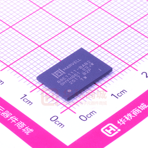
Figure 6: 88E1111 117-pin TFBGA Commercial RoHS 5/6 Compliant Package Marking and Pin 1 Location
Logo
88E1111-BAB
Country of origin (Contained in the mold ID or marked as the last line on the package.)
Lot Number YYWW xx@ Country
Part number, package code, environmental code Environmental Code - No code = RoHS 5/6 1 = RoHS 6/6 Date code, custom code, assembly plant code YYWW xx = Date code = Custom code @ = Assembly location code
Pin 1 location
Note: The above example is not drawn to scale. Location of markings is approximate.
Figure 7 is an example of the package marking and pin 1 location for the 88E1111 117-pin TFBGA Industrial RoHS 5/6 compliant package.
Figure 7: 88E1111 117-pin TFBGA Industrial RoHS 5/6 Compliant Package Marking and Pin 1 Location
L o go
88E1111-BAB
Country of origin (Contained in the mold ID or marked as the last line on the package.)
Lot Number YYWW xx@ Country
Part number, package code, environmental code Environmental Code - No code = RoHS 5/6 1 = RoHS 6/6
I
Date code, custom code, assembly plant code YYWW xx = Date code = Custom code @ = Assembly location code
Industrial Grade Package Marking Pin 1 location
Note: The above example is not drawn to scale. Location of markings is approximate.
Doc. No. MV-S105540-00, Rev. -Page 46 Document Classification: Proprietary Information
Copyright © 2009 Marvell March 4, 2009, Advance
�Order Information
Ordering Part Numbers and Package Markings
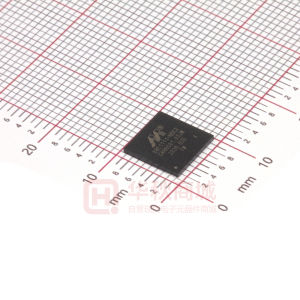
Figure 8 is an example of the package marking and pin 1 location for the 88E1111 96-pin BCC Commercial RoHS 5/6 compliant package.
Figure 8: 88E1111 96-pin BCC Commercial RoHS 5/6 Compliant Package Marking and Pin 1 Location
L o go
88E1111-CAA
Country of origin (Contained in the mold ID or marked as the last line on the package.)
Lot Number YYWW xx@ Country
Part number, package code, environmental code Environmental Code - No code = RoHS 5/6 1 = RoHS 6/6 Date code, custom code, assembly plant code YYWW xx = Date code = Custom code @ = Assembly location code
Pin 1 location
Note: The above example is not drawn to scale. Location of markings is approximate.
Figure 9 is an example of the package marking and pin 1 location for the 88E1111 96-pin BCC Industrial RoHS 5/ 6 compliant package.
Figure 9: 88E1111 96-pin BCC Industrial RoHS 5/6 Compliant Package Marking and Pin 1 Location
Logo
88E1111-CAA
Country of origin (Contained in the mold ID or marked as the last line on the package.)
Lot Number YYWW xx@ Country
Part number, package code, environmental code Environmental Code - No code = RoHS 5/6 1 = RoHS 6/6
I
Date code, custom code, assembly plant code YYWW xx = Date code = Custom code @ = Assembly location code
Industrial Grade Package Marking Pin 1 location
Note: The above example is not drawn to scale. Location of markings is approximate.
Copyright © 2009 Marvell March 4, 2009, Advance Document Classification: Proprietary Information
Doc. No. MV-S105540-00, Rev. -Page 47
�88E1111 Product Brief Integrated 10/100/1000 Ultra Gigabit Ethernet Transceiver
Figure 10 is an example of the package marking and pin 1 location for the 88E1111 128-pin PQFP Commercial RoHS 5/6 compliant package.
Figure 10: 88E1111 128-pin PQFP Commercial RoHS 5/6 Compliant Package Marking and Pin 1 Location
L o go
88E1111-RCJ
Country of origin (Contained in the mold ID or marked as the last line on the package.)
Lot Number YYWW xx@ Country
Part number, package code, environmental code Environmental Code - No code = RoHS 5/6 1 = RoHS 6/6 Date code, custom code, assembly plant code YYWW xx = Date code = Custom code @ = Assembly location code
Pin 1 location
Note: The above example is not drawn to scale. Location of markings is approximate.
Doc. No. MV-S105540-00, Rev. -Page 48 Document Classification: Proprietary Information
Copyright © 2009 Marvell March 4, 2009, Advance
�Order Information
Ordering Part Numbers and Package Markings
3.1.2 RoHS 6/6 Compliant Marking Examples
Figure 11 is an example of the package marking and pin 1 location for the 88E1111 117-pin TFBGA commercial RoHS 6/6 compliant package.
Figure 11: 88E1111 117-pin TFBGA Commercial RoHS 6/6 Compliant Package Marking and Pin 1 Location
Logo
88E1111-BAB1
Country of origin (Contained in the mold ID or marked as the last line on the package.)
Lot Number YYWW xx@ Country
Part number, package code, environmental code Environmental Code - No code = RoHS 5/6 1 = RoHS 6/6 Date code, custom code, assembly plant code YYWW xx = Date code = Custom code @ = Assembly location code
Pin 1 location
Note: The above example is not drawn to scale. Location of markings is approximate.
Figure 12 is an example of the package marking and pin 1 location for the 88E1111 117-pin TFBGA industrial RoHS 6/6 compliant package.
Figure 12: 88E1111 117-pin TFBGA Industrial RoHS 6/6 Compliant Package Marking and Pin 1 Location
Logo
88E1111-BAB1
Country of origin (Contained in the mold ID or marked as the last line on the package.)
Lot Number YYWW xx@ Country
Part number, package code, environmental code Environmental Code - No code = RoHS 5/6 1 = RoHS 6/6
I
Date code, custom code, assembly plant code YYWW xx = Date code = Custom code @ = Assembly location code
Industrial Grade Package Marking Pin 1 location
Note: The above example is not drawn to scale. Location of markings is approximate.
Copyright © 2009 Marvell March 4, 2009, Advance Document Classification: Proprietary Information
Doc. No. MV-S105540-00, Rev. -Page 49
�88E1111 Product Brief Integrated 10/100/1000 Ultra Gigabit Ethernet Transceiver
Figure 13 is an example of the package marking and pin 1 location for the 88E1111 96-pin BCC Commercial RoHS 6/6 compliant package.
Figure 13: 88E1111 96-pin BCC Commercial RoHS 6/6 Compliant Package Marking and Pin 1 Location
L o go
88E1111-CAA1
Country of origin (Contained in the mold ID or marked as the last line on the package.)
Lot Number YYWW xx@ Country
Part number, package code, environmental code Environmental Code - No code = RoHS 5/6 1 = RoHS 6/6 Date code, custom code, assembly plant code YYWW xx = Date code = Custom code @ = Assembly location code
Pin 1 location
Note: The above example is not drawn to scale. Location of markings is approximate.
Figure 14 is an example of the package marking and pin 1 location for the 88E1111 96-pin BCC Industrial RoHS 6/ 6 compliant package.
Figure 14: 88E1111 96-pin BCC Industrial RoHS 6/6 Compliant Package Marking and Pin 1 Location
L o go
88E1111-CAA1
Country of origin (Contained in the mold ID or marked as the last line on the package.)
Lot Number YYWW xx@ Country
Part number, package code, environmental code Environmental Code - No code = RoHS 5/6 1 = RoHS 6/6
I
Date code, custom code, assembly plant code YYWW xx = Date code = Custom code @ = Assembly location code
Industrial Grade Package Marking Pin 1 location
Note: The above example is not drawn to scale. Location of markings is approximate.
Doc. No. MV-S105540-00, Rev. -Page 50 Document Classification: Proprietary Information
Copyright © 2009 Marvell March 4, 2009, Advance
�Order Information
Ordering Part Numbers and Package Markings
Figure 15 is an example of the package marking and pin 1 location for the 88E1111 128-pin PQFP Commercial RoHS 6/6 compliant package.
Figure 15: 88E1111 128-pin PQFP Commercial RoHS 6/6 Compliant Package Marking and Pin 1 Location
Logo
88E1111-RCJ1
Country of origin (Contained in the mold ID or marked as the last line on the package.)
Lot Number YYWW xx@ Country
Part number, package code, environmental code Environmental Code - No code = RoHS 5/6 1 = RoHS 6/6 Date code, custom code, assembly plant code YYWW xx = Date code = Custom code @ = Assembly location code
Pin 1 location
Note: The above example is not drawn to scale. Location of markings is approximate.
Copyright © 2009 Marvell March 4, 2009, Advance Document Classification: Proprietary Information
Doc. No. MV-S105540-00, Rev. -Page 51
�Back Cover
Marvell Semiconductor, Inc. 5488 Marvell Lane Santa Clara, CA 95054, USA Tel: 1.408.222.2500 Fax: 1.408.752.9028 www.marvell.com
Marvell. Moving Forward Faster
�