1N5338B THRU 1N5388B
Features
•
Zener Voltage From 5.1V to 200V
•
Halogen Free Available Upon Request By Adding Suffix "-HF"
•
Moisture Sensitivity Level 1
•
Epoxy Meets UL 94 V-0 Flammability Rating
•
Lead Free Finish/RoHS Compliant (Note1)("P" Suffix Designates
Compliant. See Ordering Information)
5 Watt
Zener Diode
5.1 to 200 Volts
Maximum Ratings
•
•
•
•
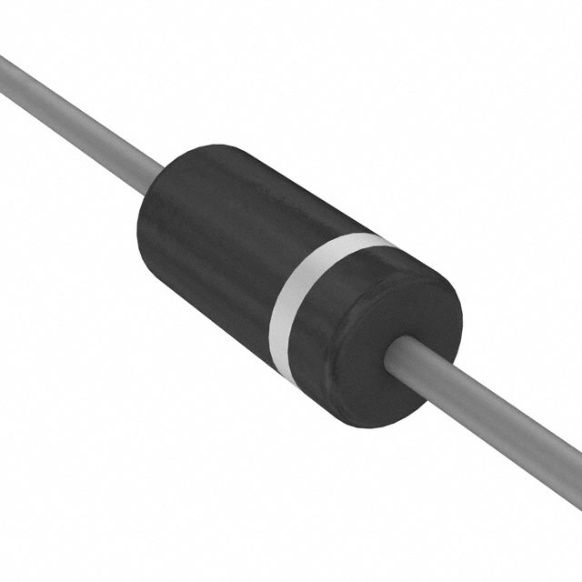
DO-15
Operating Junction Temperature Range(Note2): -55°C to +200°C
Storage Temperature Range: -55°C to +200°C
Maximum Thermal Resistence: 15oC/W from Junction to Lead
Maximum Thermal Resistence: 83oC/W from Junction to Ambient
Parameter
Power Dissipation
Symbol
PD
Power Derating
Maximum Forward
Voltage
Rating
5.0W
67mW/oC
VF
1.2V
D
Conditions
TL= 75°C
Above 75oC
A
Cathode Mark
IF=1.0A
Note:
1. High Temperature Solder Exemption Applied, See EU Directive Annex 7a.
2. Max Operating Temperature for DC Conditions is 150°C, But not to Exceed 200°C
for Pulsed Conditions With Low Duty Cycle or Non−Repetitive.
B
D
C
DIM
A
B
C
D
Rev.3-4-10082019
1/6
DIMENSIONS
INCHES
MM
MIN MAX MIN MAX
0.230 0.300 5.80 7.60
0.104 0.140 2.60 3.60
0.026 0.035 0.70 0.90
1.000 ----- 25.40 -----
NOTE
MCCSEMI.COM
�1N5338B THRU 1N5388B
Electrical Characteristics @ 25°C Unless Otherwise Specified
MCC
Part Number
1N5338B
1N5339B
1N5340B
1N5341B
1N5342B
1N5343B
1N5344B
1N5345B
1N5346B
1N5347B
1N5348B
1N5349B
1N5350B
1N5351B
1N5352B
1N5353B
1N5354B
1N5355B
1N5356B
1N5357B
1N5358B
1N5359B
1N5360B
1N5361B
1N5362B
1N5363B
1N5364B
1N5365B
1N5366B
1N5367B
1N5368B
1N5369B
1N5370B
1N5371B
1N5372B
1N5373B
1N5374B
1N5375B
1N5376B
1N5377B
1N5378B
1N5379B
1N5380B
1N5381B
1N5382B
1N5383B
1N5384B
1N5385B
1N5386B
1N5387B
1N5388B
Rev.3-4-10082019
Regulator
Voltage
VZ
V
5.1
5.6
6
6.2
6.8
7.5
8.2
8.7
9.1
10
11
12
13
14
15
16
17
18
19
20
22
24
25
27
28
30
33
36
39
43
47
51
56
60
62
68
75
82
87
91
100
110
120
130
140
150
160
170
180
190
200
Test
Current
IZ
mA
240
220
200
200
175
175
150
150
150
125
125
100
100
100
75
75
70
65
65
65
50
50
50
50
50
40
40
30
30
30
25
25
20
20
20
20
20
15
15
15
12
12
10
10
8
8
8
8
5
5
5
Maximum
Dynamic
Impedance
Maximum
Reverse
Current
Test
Voltage
Maximum
Regulator
Current
Maximum
Dynamic Knee
Impedance
Maximum
Surge
Current
ZZT
Ω
1.5
1
1
1
1
1.5
1.5
2
2
2
2.5
2.5
2.5
2.5
2.5
2.5
2.5
2.5
3
3
3.5
3.5
4
5
6
8
10
11
14
20
25
27
35
40
42
44
45
65
75
75
90
125
170
190
230
330
350
380
430
450
480
IR
µA
1
1
1
1
10
10
10
10
7.5
5
5
2
1
1
1
1
0.5
0.5
0.5
0.5
0.5
0.5
0.5
0.5
0.5
0.5
0.5
0.5
0.5
0.5
0.5
0.5
0.5
0.5
0.5
0.5
0.5
0.5
0.5
0.5
0.5
0.5
0.5
0.5
0.5
0.5
0.5
0.5
0.5
0.5
0.5
VR
V
1
2
3
3
5.2
5.7
6.2
6.6
6.9
7.6
8.4
9.1
9.9
10.6
11.5
12.2
12.9
13.7
14.4
15.2
16.7
18.2
19
20.6
21.2
22.8
25.1
27.4
29.7
32.7
35.8
38.8
42.6
45.5
47.1
51.7
56
62.2
66
69.2
76
83.6
91.2
98.8
106
114
122
129
137
144
152
IZM
mA
930
865
790
765
700
630
580
545
520
475
430
395
365
340
315
295
280
264
250
237
216
198
190
176
170
158
144
132
122
110
100
93
86
79
76
70
63
58
54.5
52.5
47.5
43
39.5
36.6
34
31.6
29.4
28
26.4
25
23.6
ZZK @1.0mA
Ω
400
400
300
200
200
200
200
200
150
125
125
125
100
75
75
75
75
75
75
75
75
100
110
120
130
140
150
160
170
190
210
230
280
350
400
500
620
720
760
760
800
1000
1150
1250
1500
1500
1650
1750
1750
1850
1850
IZSM
A
14.4
13.4
12.7
12.4
11.5
10.7
10
9.5
9.2
8.6
8
7.5
7
6.7
6.3
6
5.8
5.5
5.3
5.1
4.7
4.4
4.3
4.1
3.9
3.7
3.5
3.3
3.1
2.8
2.7
2.5
2.3
2.2
2.1
2
1.9
1.8
1.7
1.6
1.5
1.4
1.3
1.2
1.2
1.1
1.1
1
1
0.9
0.9
2/6
Maximum
Voltage
Regulation
V
0.39
0.25
0.19
0.1
0.15
0.15
0.2
0.2
0.22
0.22
0.25
0.25
0.25
0.25
0.25
0.3
0.35
0.4
0.4
0.4
0.45
0.55
0.55
0.6
0.6
0.6
0.6
0.65
0.65
0.7
0.8
0.9
1
1.2
1.35
1.5
1.6
1.8
2
2.2
2.3
2.5
2.5
2.5
2.5
3
3
3
4
5
5
MARKING
CODE
1N5338B
1N5339B
1N5340B
1N5341B
1N5342B
1N5343B
1N5344B
1N5345B
1N5346B
1N5347B
1N5348B
1N5349B
1N5350B
1N5351B
1N5352B
1N5353B
1N5354B
1N5355B
1N5356B
1N5357B
1N5358B
1N5359B
1N5360B
1N5361B
1N5362B
1N5363B
1N5364B
1N5365B
1N5366B
1N5367B
1N5368B
1N5369B
1N5370B
1N5371B
1N5372B
1N5373B
1N5374B
1N5375B
1N5376B
1N5377B
1N5378B
1N5379B
1N5380B
1N5381B
1N5382B
1N5383B
1N5384B
1N5385B
1N5386B
1N5387B
1N5388B
MCCSEMI.COM
�1N5338B THRU 1N5388B
Remarks:
1. TOLERANCE AND VOLTAGE DESIGNATION - The JEDEC type numbers shown indicate a tolerance of+/-10% with
guaranteed limits on only Vz, IR, Ir, and VF as shown in the electrical characteristics table. Units with guaranteed limits
on all seven parameters are indicated by suffix “B” for+/-5% tolerance.
2. ZENER VOLTAGE (Vz) AND IMPEDANCE (ZZT & ZZK) - Test conditions for Zener voltage and impedance are as
follows; Iz is applied 40+/-10 ms prior to reading. Mounting contacts are located from the inside edge of mounting
clips to the body of the diode(Ta=25 C)
o
3. SURGE CURRENT (Ir) - Surge current is specified as the maximum allowable peak, non-recurrent square-wave
current with a pulse width, PW, of 8.3 ms. The data given in Figure 5 may be used to find the maximum surge
current for a quare wave of any pulse width between 1 ms and 1000ms by plotting the applicable points on
logarithmic paper. Examples of this, using the 6.8v , is shown in Figure 6. Mounting
contact located as specified in Note 3. (TA=25 ć ).
4. VOLTAGE REGULATION (Vz) - Test conditions for voltage regulation are as follows: Vz measurements are made
at 10% and then at 50% of the Iz max value listed in the electrical characteristics table. The test currents are the
same for the 5% and 10% tolerance devices. The test current time druation for each Vz measurement is 40+/- 10 ms.
(TA=25C ). Mounting contact located as specified in Note2.
5. MAXIMUM REGULATOR CURRENT (IZM) - The maximum current shown is based on the maximum voltage of a
5% type unit. Therefore, it applies only to the B-suffix device. The actual IZM for any device may not exceed the
value of 5 watts divided by the actual Vz of the device. TL=75Cat maximum from the device body.
APPLICATION NOTE:
Since the actual voltage available from a given Zener
diode is temperature dependent, it is necessary to determine
junction temperature under any set of operating conditions
in order to calculate its value. The following procedure is
recommended:
Lead Temperature, TL, should be determined from:
TL = qLA PD + TA
qLA is the lead‐to‐ambient thermal resistance and PD is the
power dissipation.
Junction Temperature, TJ, may be found from:
TJ = TL + DTJL
DTJL is the increase in junction temperature above the lead
temperature and may be found from Figure 7 for a train of
power pulses or from Figure 1 for dc power.
DTJL = qJL PD
Rev.3-4-10082019
3/6
For worst‐case design, using expected limits of IZ, limits
of PD and the extremes of TJ (DTJ) may be estimated.
Changes in voltage, VZ, can then be found from:
DV = qVZ DTJ
qVZ, the Zener voltage temperature coefficient.
Under high power‐pulse operation, the Zener voltage will
vary with time and may also be affected significantly by the
zener resistance. For best regulation, keep current
excursions as low as possible.
Data of Figure 7 should not be used to compute surge
capability. Surge limitations are given in Figure 5. They are
lower than would be expected by considering only junction
temperature, as current crowding effects cause temperatures
to be extremely high in small spots resulting in device
degradation should the limits of Figure 5 be exceeded.
MCCSEMI.COM
�1N5338B THRU 1N5388B
Curve Characteristics
Fig. 1 - Power Derating Curve
Fig. 2 - Typical Zener Breakdown Characteristics
10000
6
VZ - 6.0 thru 10 Volts
1000
Zener Current (mA)
Power Dissipation (W)
5
4
3
2
100
10
1
1
0
0
25
50
75
100
125
0.1
150
0
1
2
3
4
Fig. 3 - Typical Zener Breakdown Characteristics
6
7
8
9
10
11
Fig. 4 - Typical Zener Breakdown Characteristics
1000
1000
VZ - 11 thru 75 Volts
500
5
Zener Voltage (V)
Lead Temperature (°C)
VZ - 82 thru 200 Volts
200
100
50
Zener Current (mA)
Zener Current (mA)
100
20
10
5
2
10
1
1
0.5
0.2
0.1
10
20
30
40
50
60
70
0.1
80
80
100
120
140
160
180
Fig. 5 - Surge Current Characteristics
220
Fig. 6 - Peak Surge Current VS Pulse Width
30
40
VZ=6.8V
PW=1ms
10
10
PW=8.3ms
Peak Surge Current (A)
Peak Surge Current (A)
200
Zener Voltage (V)
Zener Voltage (V)
1
PW=1000ms
Plotted From Information Given in Figure 5
1
Sine / Square Wave PW=100ms
0.1
0.1
3
10
100
200
Rev.3-4-10082019
1
10
100
1000
Pulse Width (ms)
Nominal Zener Voltage (V)
4/6
MCCSEMI.COM
�1N5338B THRU 1N5388B
Curve Characteristics
Fig. 7 - Typical Thermal Resistace
O
Junction to Lead Thermal Resistance (C /W)
40
30
20
10
MOUNT ON 8.0mm2 Copper Pads to Each Terminal
0
0.0
0.2
0.4
0.6
0.8
1.0
Lead Length to Heat Sink (inch)
Rev.3-4-10082019
5/6
MCCSEMI.COM
�1N5338B THRU 1N5388B
Ordering Information
Device
Packing
(Part Number)-TP
Tape&Reel: 4Kpcs/Reel
(Part Number)-AP
Ammo Packing: 3Kpcs/Ammo Box
(Part Number)-BP
Bulk: 25Kpcs/Carton
Note : Adding "-HF" Suffix For Halogen Free, eg. Part Number-TP-HF
***IMPORTANT NOTICE***
Micro Commercial Components Corp. reserves the right to make changes without further notice to any product herein to
make corrections, modifications , enhancements , improvements , or other changes . Micro Commercial Components�
Corp . does not assume any liability arising out of the application or use of any product described herein; neither does it
convey any license under its patent rights ,nor the rights of others . The user of products in such applications shall assume all
risks of such use and will agree to hold Micro Commercial Components Corp . and all the companies whose products are
represented on our website, harmless against all damages.
***LIFE SUPPORT***
MCC's products are not authorized for use as critical components in life support devices or systems without the express
written approval of Micro Commercial Components Corporation.
***CUSTOMER AWARENESS***
Counterfeiting of semiconductor parts is a growing problem in the industry. Micro Commercial Components (MCC) is taking
strong measures to protect ourselves and our customers from the proliferation of counterfeit parts. MCC strongly encourages
customers to purchase MCC parts either directly from MCC or from Authorized MCC Distributors who are listed by country on
our web page cited below. Products customers buy either from MCC directly or from Authorized MCC Distributors are genuine
parts, have full traceability, meet MCC's quality standards for handling and storage. MCC will not provide any warranty
coverage or other assistance for parts bought from Unauthorized Sources. MCC is committed to combat this global
problem and encourage our customers to do their part in stopping this practice by buying direct or from authorized
distributors.
Rev.3-4-10082019
6/6
MCCSEMI.COM
�
很抱歉,暂时无法提供与“1N5352B-TP”相匹配的价格&库存,您可以联系我们找货
免费人工找货- 国内价格 香港价格
- 4000+1.180944000+0.15290
- 8000+1.078208000+0.13960
- 12000+1.0258212000+0.13282
- 20000+0.9669820000+0.12520
- 28000+0.9321228000+0.12069
- 40000+0.8982640000+0.11630
- 国内价格
- 20+0.21384
- 200+0.16838
- 600+0.14310
- 4000+0.12798
- 8000+0.11481
- 20000+0.10768
- 国内价格 香港价格
- 1+5.469821+0.70818
- 10+3.3863910+0.43844
- 100+2.15317100+0.27877
- 500+1.62012500+0.20976
- 1000+1.447991000+0.18748
- 2000+1.303042000+0.16871