MCC
• • • • •
���������� ���
���omponents 20736 Marilla Street Chatsworth �������� ���� ������ �!��"#��� $
%�� � � ���� �!��"#���
2N7002V
Features
Dual N-Channel MOSFET Low On-Resistance Low Gate Threshold Voltage Low Input Capacitance Fast Switching Speed
Symbol VDSS VDGR VGSS ID PD RθJA TJ TSTG Rating Drain-source Voltage Drain-Gate Voltage Gate-source Voltage Drain Current Total Power Dissipation Thermal Resistance Junction to Ambient Operating Junction Temperature Storage Temperature Rating 60 60 ±20 280 150 833 -55 to +150 -55 to +150 Unit V V V mA mW ℃/W ℃ ℃ Max --2.5 ±0.1 1 500 --3.0 2.0 --50 25 5 Units Vdc Vdc µAdc µAdc
DIMENSIONS
N-Channel MOSFET
Maximum Ratings @ 25OC Unless Otherwise Specified
SOT-563
Electrical Characteristics @ 25OC Unless Otherwise Specified
Symbol V(BR)DSS Vth(GS) IGSS IDSS Parameter Drain-Source Breakdown Voltage* (VGS=0Vdc, ID=10µAdc) Gate-Threshold Voltage* (VDS=VGS, ID=250µAdc) Gate-body Leakage* (VDS =0Vdc, VGS =±20Vdc) Zero Gate Voltage Drain Current* (VDS =60Vdc, VGS =0Vdc) (VDS =0Vdc, VGS =±20Vdc, Tj=125℃) On-state Drain Current* (VDS =7.5Vdc, VGS =10Vdc) Drain-Source On-Resistance* (VGS=5Vdc, ID=50mAdc) (VGS=10Vdc, ID=500mAdc) Forward Tran Conductance* (VDS=10Vdc, ID=200mAdc) Input Capacitance VDS=25Vdc, Output Capacitance VGS =0Vdc Reverse Transfer f=1MHz Capacitance Min 60 1.0 ------0.5 ----80 ------Typ 70 --------1.0 -------------
ID(ON) rDS(on)
Adc Ω ms
DIM A B C D G H K L M
INCHES MIN .006 .043 .061 .020 .035 .059 .022 .004 .004 .043 .067 .023 .011 .007 0.90 1.50 0.56 0.10 0.10 MAX .011 .049 .067 MIN 0.15 1.10 1.55
MM MAX 0.30 1.25 1.70 0.50 1.10 1.70 0.60 0.30 0.18 NOTE
gFS Ciss COSS CrSS
pF
Switching
VDD=30Vdc, VGEN=10Vdc RL=150Ω,ID=200mA, td(off) Turn-off Time RG=25Ω * Pulse test, pulse width≦300μs, duty cycle≦20% td(on) Turn-on Time --------20 ns 20
Revision: 1
www.mccsemi.com
2005/01/25
�2N7002V
MCC
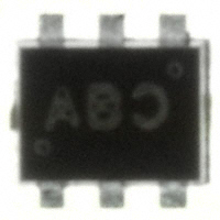
Marking: KAS
Revision: 1
www.mccsemi.com
2005/01/25
�
很抱歉,暂时无法提供与“2N7002V”相匹配的价格&库存,您可以联系我们找货
免费人工找货