MCC
Features
• •
���������� ���
���omponents 21201 Itasca Street Chatsworth �������� ���� ������ �!��"#��� $
%�� � � ���� �!��"#���
MMBT3906
Surface Mount SOT-23 Package Capable of 350mWatts of Power Dissipation
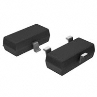
C Pin Configuration Top View
PNP General Purpose Amplifier
SOT-23
A D
2A
B E Min 40 40 5.0 50 50 Max Units Vdc Vdc Vdc nAdc nAdc
G H J F E C B
Electrical Characteristics @ 25°C Unless Otherwise Specified
Symbol Parameter Collector-Emitter Breakdown Voltage* (I C=1.0mAdc, IB=0) Collector-Base Breakdown Voltage (I C=10µ Adc, IE=0) Emitter-Base Breakdown Voltage (I E=10µ Adc, IC=0) Base Cutoff Current (VCE=30Vdc, VBE=3.0Vdc) Collector Cutoff Current (VCE=30Vdc, VBE=3.0Vdc) DC Current Gain* (I C=0.1mAdc, VCE=1.0Vdc) (I C=1.0mAdc, VCE=1.0Vdc) (I C=10mAdc, VCE=1.0Vdc) (I C=50mAdc, VCE=1.0Vdc) (I C=100mAdc, VCE=1.0Vdc) Collector-Emitter Saturation Voltage (I C=10mAdc, IB=1.0mAdc) (I C=50mAdc, IB=5.0mAdc) Base-Emitter Saturation Voltage (I C=10mAdc, IB=1.0mAdc) (I C=50mAdc, IB=5.0mAdc) Current Gain-Bandwidth Product (I C=10mAdc, VCE=20Vdc, f=100MHz) Output Capacitance (VCB=5.0Vdec, IE=0, f=1.0MHz) Input Capacitance (VBE=0.5Vdc, IC=0, f=1.0MHz) Noise Figure (IC=100µ Adc, VCE=5.0Vdc, RS=1.0kΩ f=10Hz to 15.7kHz) Delay Time (VCC=3.0Vdc, VBE=0.5Vdc Rise Time IC=10mAdc, IB1=1.0mAdc) Storage Time (VCC=3.0Vdc, IC=10mAdc Fall Time IB1=IB2=1.0mAdc) ≤ 300µ s, Duty Cycle ≤ 2.0%
OFF CHARACTERISTICS
V(BR)CEO V(BR)CBO V(BR)EBO IBL ICEX
ON CHARACTERISTICS
hFE
K
60 80 100 60 30
DIMENSIONS
300
VCE(sat)
0.25 0.4 0.65 0.85 0.95
Vdc
VBE(sat)
Vdc
SMALL-SIGNAL CHARACTERISTICS
fT Cobo Cibo NF 250 4.5 10.0 4.0 MHz pF pF dB
DIM A B C D E F G H J K
INCHES MIN .110 .083 .047 .035 .070 .018 .0005 .035 .003 .015
MAX .120 .098 .055 .041 .081 .024 .0039 .044 .007 .020
MM MIN 2.80 2.10 1.20 .89 1.78 .45 .013 .89 .085 .37
MAX 3.04 2.64 1.40 1.03 2.05 .60 .100 1.12 .180 .51
NOTE
Suggested Solder Pad Layout
.031 .800 .035 .900 .079 2.000 inches mm
SWITCHING CHARACTERISTICS
td tr ts tf *Pulse Width 35 35 225 75 ns ns ns ns
.037 .950 .037 .950
www.mccsemi.com
�MMBT3906
DC Current Gain vs Collector Current 220 VCE = 1.0V 200 160 hFE 120 80 40 VBE(ON) - (V) 0.6 0.4 0.2 0 0.1 TA = 100°C 1.2 1.0 0.8 TA = 25°C
MCC
Base-Emitter ON Voltage vs Collector Current VCE = 5.0V
0.1
1 IC (mA)
10
100
1.0 IC - (mA)
10
100
Collector-Emitter Saturation Volatge vs Collector Current 0.6 0.5 0.4 VCE(SAT) - (V) 0.3 0.2 0.1 0 1.0 VBE(SAT) - (V) IC/IB = 10 TA = 25°C 1.4 1.2 1.0 0.8 0.6 0.4
Base-Emitter Saturation Voltage vs Collector Current IC/IB = 10 TA = 25°C
10 IC - (mA)
100
1000
0.2 1.0
10 IC - (mA)
100
1000
Collector-Base Diode Reverse Current vs Temperature 100
Common Base Open Circuit Input and Output Capacitance vs Reverse Bias Voltage 1.0 COBO TA = 25°C TO-92 8
VCB = 20V 10 ICBO - (mA) 1.0 2 0.1 0 25 50 75 TJ - (°C) 100 125 150 0 0.1 pF 6 CIBO 4
1.0 Volts - (V)
10
www.mccsemi.com
�MMBT3906
Maximum Power Dissipation vs Ambient Temperature 800 12 10 600 TO-92 PD(MAX) - (mW) 400 NF - (dB) 6 4 200 SOT-23 0 0 50 100 TA - (°C) Contours of Constant Gain Bandwidth Product (fT) 24 20 16 VCE - (V) 12 8 4 0 0.1 10 0.1 hfe 100 1000 150 200 2 0 0.1 8 IC = 1.0mA Noise Figure vs Source Resistance
MCC
VCE = 5.0V f = 1.0kHz
IC = 100µ A
1.0
10 RS - (kΩ)
100
Current Gain VCE = 10V f = 1.0kHz
10 100 IC - (mA) *100MHz increments from 100 to 700, 750 and 800MHz
1.0
1.0 IC - (mA)
10
Noise Figure vs Frequency 6 VCE = 5.0V 5 1000
Switching Times vs Collector Current IB1 = IB2 = IC/10 ts
4 NF - (dB) 3 2 1 0 IC = 100µ A RS = 200Ω T - (ns)
100 tf
IC = 1.0mA RS = 200Ω IC = 100µ A RS = 2.0kΩ
10
tr td
0.1
1.0 f - (kHz)
10
100
1.0 1.0
10 IC - (mA)
100
www.mccsemi.com
�MMBT3906
Input Impedance 10 VCE = 10V f = 1.0kHz 1000 Output Admittance
MCC
VCE = 10V f = 1.0kHz hoe - (µΩ) 100
hie - (kΩ) 1.0
0.1 0.1
10 1.0 IC - (mA) 10 0.1 1.0 IC - (mA) 10
Voltage Feedback Ratio 100 1000
Turn On and Turn Off Times vs Collector Current
hfe - (X10 ) 10 T - (ns)
-4
100
toff
ton 10 ton IB1 = IC/10 VBE(OFF) = 0.5V toff IB1 = IB2 = IC/10 10 IC - (mA) 100
1.0 0.1 1.0 IC - (mA) 10
1.0 1.0
www.mccsemi.com
�
很抱歉,暂时无法提供与“MMBT3906”相匹配的价格&库存,您可以联系我们找货
免费人工找货