MCC
Features
• •
���������� ���
���omponents 21201 Itasca Street Chatsworth �������� ���� ������ �!��"#��� $
%�� � � ���� �!��"#���
MMBTA42
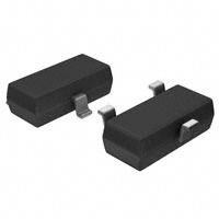
Surface Mount SOT-23 Package Capable of 300mWatts of Power Dissipation
C Pin Configuration Top View
NPN Silicon High Voltage Transistor
SOT-23
A D
1D
B E Min 300 300 6.0 0.1 0.1 Max Units Vdc Vdc Vdc uAdc uAdc
G H J F E C B
Electrical Characteristics @ 25°C Unless Otherwise Specified
Symbol Parameter Collector-Emitter Breakdown Voltage* (I C=1.0mAdc, IB=0) Collector-Base Breakdown Voltage (I C=100µ Adc, IE=0) Emitter-Base Breakdown Voltage (I E=100µ Adc, IC=0) Collector Cutoff Current (VCB=200Vdc, IE=0) Emitter Cutoff Current (VEB=6.0Vdc, IC=0) DC Current Gain* (I C=1.0mAdc, VCE=10Vdc) (I C=10mAdc, VCE=10Vdc) (I C=30mAdc, VCE=10Vdc) VCE(sat) Collector-Emitter Saturation Voltage (I C=20mAdc, IB=2.0mAdc) Base-Emitter Saturation Voltage (I C=20mAdc, IB=2.0mAdc) 25 40 40
OFF CHARACTERISTICS
V(BR)CEO V(BR)CBO V(BR)EBO ICBO IEBO
ON CHARACTERISTICS
hFE
K DIMENSIONS
----
0.5
Vdc
VBE(sat)
0.9
Vdc
SMALL-SIGNAL CHARACTERISTICS
fT Ccb Current Gain-Bandwidth Product (I C=10mAdc, VCE=20Vdc, f=100MHz) Collector-Emitter Capacitance (VCB=20Vdec, IE=0, f=1.0MHz) 50 3.0 MHz pF
DIM A B C D E F G H J K
INCHES MIN .110 .083 .047 .035 .070 .018 .0005 .035 .003 .015
MAX .120 .098 .055 .041 .081 .024 .0039 .044 .007 .020
MM MIN 2.80 2.10 1.20 .89 1.78 .45 .013 .89 .085 .37
MAX 3.04 2.64 1.40 1.03 2.05 .60 .100 1.12 .180 .51
NOTE
Suggested Solder Pad Layout
.031 .800 .035 .900 .079 2.000 inches mm
THERMAL CHARACTERISTICS
Characteristic Total Device Dissipation FR–5 Board,(1) TA = 25°C Derate above 25°C Thermal Resistance, Junction to Ambient Total Device Dissipation Alumina Substrate,(2) TA = 25°C Derate above 25°C Thermal Resistance, Junction to Ambient Junction and Storage Temperature
*Pulse Width ≤ 300µ s, Duty Cycle ≤ 2.0%
Symbol PD
Max 225 1.8
Unit mW mW/°C °C/W mW mW/°C °C/W °C
RqJA PD
556 300 2.4
.037 .950 .037 .950
RqJA TJ, Tstg
417 –55 to +150
www.mccsemi.com
�MMBTA42
120 100 hFE , DC CURRENT GAIN 80 60 40 20 0 25°C TJ = +125°C
MCC
VCE = 10 Vdc
-55°C
0.1
1.0 IC, COLLECTOR CURRENT (mA)
10
100
Figure 1. DC Current Gain
Ceb @ 1MHz C, CAPACITANCE (pF) 10
BANDWIDTH (MHz) f T, CURRENT-GAIN
100
80 70 60 50 40 30 20 10 1.0 2.0 3.0 5.0 7.0 10 20 30 IC, COLLECTOR CURRENT (mA) TJ = 25°C VCE = 20 V f = 20 MHz 50 70 100
1.0
Ccb @ 1MHz
0.1 0.1
1.0 10 100 VR, REVERSE VOLTAGE (VOLTS)
1000
Figure 2. Capacitance
Figure 3. Current–Gain – Bandwidth
1.4 1.2 V, VOLTAGE (VOLTS) 1.0 0.8 0.6 0.4 0.2 0.0 0.1 1.0 10 IC, COLLECTOR CURRENT (mA) 100 VCE(sat) @ 25°C, IC/IB = 10 VCE(sat) @ 125°C, IC/IB = 10 VCE(sat) @ -55°C, IC/IB = 10 VBE(sat) @ 25°C, IC/IB = 10 VBE(sat) @ 125°C, IC/IB = 10 VBE(sat) @ -55°C, IC/IB = 10 VBE(on) @ 25°C, VCE = 10 V VBE(on) @ 125°C, VCE = 10 V VBE(on) @ -55°C, VCE = 10 V
Figure 4. ”ON” Voltages
www.mccsemi.com
�
很抱歉,暂时无法提供与“MMBTA42”相匹配的价格&库存,您可以联系我们找货
免费人工找货- 国内价格
- 10+0.32522
- 100+0.21681
- 600+0.18582