MCC
TM
Micro Commercial Components
���������� ���
���omponents 20736 Marilla Street Chatsworth �������� ���� ������ �!��"#��� $
%�� � � ���� �!��"#���
SI2302
Features
• • • • • • •
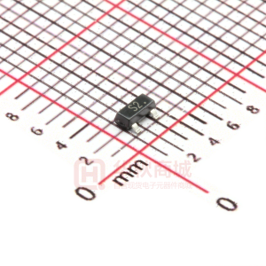
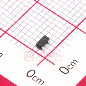
20V,3.0A, RDS(ON)=55m¡@VGS=4.5V RDS(ON)=82m¡@VGS=2.5V High dense cell design for extremely low RDS(ON) Rugged and reliable Lead free product is acquired SOT-23 Package Marking Code: S2 Case Material: Molded Plastic. UL Flammability Classification Rating 94V-0
Parameter Drain-source Voltage Drain Current-Continuous Drain Current-Pulsed a Gate-source Voltage Total Power Dissipation Thermal Resistance Junction to Ambientb Operating Junction Temperature Storage Temperature Rating 20 3 10 f8 1.25 100 -55 to +150 -55 to +150 Unit V A A V W /W
N-Channel Enhancement Mode Field Effect Transistor
SOT-23
A D
Maximum Ratings @ 25OC Unless Otherwise Specified
Symbol VDS ID IDM VGS PD R©JA TJ TSTG
3
1.GATE
C B
2. SOURCE 3. DRAIN
1
F E
2
G K
H
J
DIMENSIONS INCHES MIN .110 .083 .047 .035 .070 .018 .0005 .035 .003 .015 MM MIN 2.80 2.10 1.20 .89 1.78 .45 .013 .89 .085 .37
Internal Block Diagram
D
DIM A B C D E F G H J K
MAX .120 .098 .055 .041 .081 .024 .0039 .044 .007 .020
MAX 3.04 2.64 1.40 1.03 2.05 .60 .100 1.12 .180 .51
NOTE
Suggested Solder Pad Layout
G
.035 .900 .031 .800
S
.079 2.000
inches mm
.037 .950 .037 .950
www.mccsemi.com
Revision: 1
1 of 5
2008/01/01
�MCC
TM
Micro Commercial Components
SI2302
TA = 25 C unless otherwise noted Symbol BVDSS IDSS IGSSF IGSSR VGS(th) RDS(on) gFS Ciss Coss Crss td(on) tr td(off) tf Qg Qgs Qgd IS VSD VGS = 0V, IS = 0.94A VDS = 10V, ID = 3.6A, VGS = 4.5V VDD = 10V, ID = 3.6A, VGS = 4.5V, RGEN = 6Ω Test Condition VGS = 0V, ID = 10µA VDS = 20V, VGS = 0V VGS = 8V, VDS = 0V VGS = -8V, VDS = 0V VGS = VDS, ID = 50µA VGS = 4.5V, ID = 3.6A VGS = 2.5V, ID = 3.1A VDS = 5V, ID = 3.6A 0.65 55 82 8.5 237 120 45 23 11 34 36 6 1.4 1.8 0.94 1.2 45 30 70 70 10 Min 20 1 100 -100 1.2 72 110 Typ Max Units V
µA
Electrical Characteristics
Parameter Off Characteristics Drain-Source Breakdown Voltage Zero Gate Voltage Drain Current Gate Body Leakage Current, Forward Gate Body Leakage Current, Reverse On Characteristics Static Drain-Source On-Resistance Forwand Transconductance Dynamic Characteristics d Input Capacitance Output Capacitance Reverse Transfer Capacitance Switching Characteristics d Turn-On Delay Time Turn-On Rise Time Turn-Off Delay Time Turn-On Fall Time Total Gate Charge Gate-Source Charge Gate-Drain Charge Drain-Source Diode Forward Current b Drain-Source Diode Forward Voltage c
c
nA nA V mΩ mΩ S pF pF pF ns ns ns ns nC nC nC A V
Gate Threshold Voltage
VDS = 10V, VGS = 0V, f = 1.0 MHz
Drain-Source Diode Characteristics and Maximun Ratings
Notes : a.Repetitive Rating : Pulse width limited by maximum junction temperature. b.Surface Mounted on FR4 Board, t < 10 sec. c.Pulse Test : Pulse Width < 300µs, Duty Cycle < 2%. d.Guaranteed by design, not subject to production testing.
www.mccsemi.com
Revision: 1
2 of 5
2008/01/01
�MCC
TM
Micro Commercial Components
SI2302
10 25 C
10 VGS=4.5,3.5,2.5V
ID, Drain Current (A)
6
ID, Drain Current (A)
8
8
6
VGS=2.0V
4
4
2 0 0 1 2 3
VGS=1.5V
2 TJ=125 C 0 -55 C 2 3
4
5
0
1
VDS, Drain-to-Source Voltage (V) Figure 1. Output Characteristics
600 500 400 300 Ciss 200 Coss 100 0 0 5 10 15 20 25 Crss 2.2 1.9 1.6 1.3 1.0 0.7 0.4 -100
VGS, Gate-to-Source Voltage (V) Figure 2. Transfer Characteristics
RDS(ON), Normalized RDS(ON), On-Resistance(Ohms)
ID=3.6A VGS=4.5V
C, Capacitance (pF)
-50
0
50
100
150
200
VDS, Drain-to-Source Voltage (V) Figure 3. Capacitance
1.3 1.2 1.1 1.0 0.9 0.8 0.7 0.6 -50
TJ, Junction Temperature( C) Figure 4. On-Resistance Variation with Temperature
VGS=0V
1
VTH, Normalized Gate-Source Threshold Voltage
VDS=VGS ID=250µA
IS, Source-drain current (A)
25 50 75 100 125 150
10
10
0
10 -25 0
-1
0.2
0.4
0.6
0.8
1.0
1.2
TJ, Junction Temperature( C) Figure 5. Gate Threshold Variation with Temperature
VSD, Body Diode Forward Voltage (V) Figure 6. Body Diode Forward Voltage Variation with Source Current
www.mccsemi.com
Revision: 1
3 of 5
2008/01/01
�MCC
TM
Micro Commercial Components
SI2302
ID, Drain Current (A)
10
1
VGS, Gate to Source Voltage (V)
5 V =10V DS ID=3.6A 4
RDS(ON)Limit 1ms 10ms 100ms 1s DC
3
10
0
2
10
-1
1
0 0 2 4 6
10
-2
TA=25 C TJ=150 C Single Pulse 10
-1
10
0
10
1
10
2
Qg, Total Gate Charge (nC) Figure 7. Gate Charge
VDS, Drain-Source Voltage (V) Figure 8. Maximum Safe Operating Area
VDD t on V IN D VGS RGEN G
90%
toff tr
90%
RL VOUT
td(on) VOUT
td(off)
90% 10%
tf
10%
INVERTED
S
VIN
50% 10%
50%
PULSE WIDTH
Figure 9. Switching Test Circuit
Figure 10. Switching Waveforms
r(t),Normalized Effective Transient Thermal Impedance
10
0
D=0.5
0.2
10
-1
0.1 0.05 0.02 Single Pulse
-4
PDM t1 t2 1. R JA (t)=r (t) * R JA 2. R JA=See Datasheet 3. TJM-TA = P* R JA (t) 4. Duty Cycle, D=t1/t2
10
-2
10
10
-3
10
-2
10
-1
10
0
10
1
10
2
Square Wave Pulse Duration (sec) Figure 11. Normalized Thermal Transient Impedance Curve
www.mccsemi.com
Revision: 1
4 of 5
2008/01/01
�MCC
Micro Commercial Components
TM
Ordering Information
Device (Part Number)-TP Packing Tape&Reel;3Kpcs/Reel
***IMPORTANT NOTICE*** Micro Commercial Components Corp . reserves the right to make changes without further notice to any product herein to make corrections, modifications , enhancements , improvements , or other changes . Micro Commercial Components Corp . does not assume any liability arising out of the application or use of any product described herein; neither does it convey any license under its patent rights ,nor the rights of others . The user of products in such applications shall assume all risks of such use and will agree to hold Micro Commercial Components Corp . and all the companies whose products are represented on our website, harmless against all damages. ***APPLICATIONS DISCLAIMER*** Products offer by Micro Commercial Components Corp . are not intended for use in Medical, Aerospace or Military Applications.
www.mccsemi.com
Revision: 1
5 of 5
2008/01/01
�