MX25V1006F
MX25V1006F
1M-BIT [x 1/x 2] CMOS SERIAL NOR FLASH
Key Features
• Voltlage Range VCC: 2.3V - 3.6V
• Dual I/O Supported
• Auto Erase and Auto Program Algorithm
• Low Power Consumption
P/N: PM2424
1
Rev. 1.0, April 20, 2017
�MX25V1006F
Contents
1. FEATURES............................................................................................................................................................... 4
GENERAL.............................................................................................................................................................. 4
PERFORMANCE................................................................................................................................................... 4
SOFTWARE FEATURES....................................................................................................................................... 4
HARDWARE FEATURES....................................................................................................................................... 4
2. GENERAL DESCRIPTION...................................................................................................................................... 5
3. PIN CONFIGURATIONS........................................................................................................................................... 6
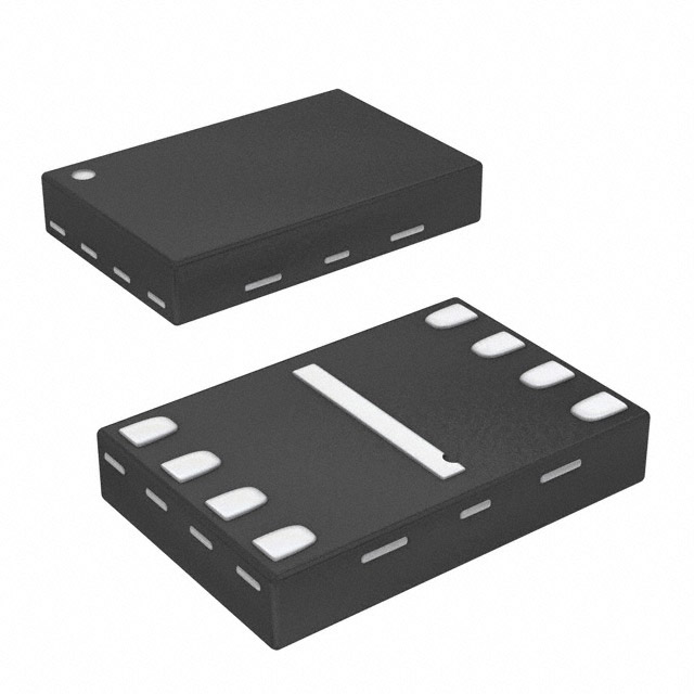
8-LAND USON (2x3mm) ....................................................................................................................................... 6
8-PIN TSSOP (173mil) .......................................................................................................................................... 6
8-PIN SOP (150mil) ............................................................................................................................................... 6
4. PIN DESCRIPTION................................................................................................................................................... 6
5. BLOCK DIAGRAM.................................................................................................................................................... 7
6. DATA PROTECTION................................................................................................................................................. 8
Table 1. Protected Area Sizes................................................................................................................................ 8
7. MEMORY ORGANIZATION...................................................................................................................................... 9
Table 2. Memory Organization .............................................................................................................................. 9
8. DEVICE OPERATION............................................................................................................................................. 10
9. Timing Analysis..................................................................................................................................................... 11
Table 3. COMMAND DESCRIPTION................................................................................................................... 12
9-1. Write Enable (WREN)............................................................................................................................... 13
9-2. Write Disable (WRDI)................................................................................................................................ 14
9-3. Read Identification (RDID)........................................................................................................................ 15
9-4. Read Electronic Signature (RES)............................................................................................................. 16
9-5. Read Electronic Manufacturer ID & Device ID (REMS)............................................................................ 17
9-6. ID Read..................................................................................................................................................... 18
Table 4. ID Definitions ......................................................................................................................................... 18
9-7. Read Status Register (RDSR).................................................................................................................. 19
Status Register..................................................................................................................................................... 21
Table 5. Status Register....................................................................................................................................... 21
9-8. Write Status Register (WRSR).................................................................................................................. 22
Table 6. Protection Modes.................................................................................................................................... 23
9-9. Read Data Bytes (READ)......................................................................................................................... 26
9-10. Read Data Bytes at Higher Speed (FAST_READ)................................................................................... 27
9-11. Dual Read Mode (DREAD)....................................................................................................................... 28
9-12. 2 x I/O Read Mode (2READ).................................................................................................................... 29
9-13. Sector Erase (SE)..................................................................................................................................... 30
9-14. Block Erase (BE32K)................................................................................................................................ 31
9-15. Block Erase (BE)...................................................................................................................................... 32
9-16. Chip Erase (CE)........................................................................................................................................ 33
9-17. Page Program (PP).................................................................................................................................. 34
9-18. Deep Power-down (DP)............................................................................................................................ 35
9-19. Release from Deep Power-down (RDP), Read Electronic Signature (RES)............................................ 36
9-20. Software Reset - Reset-Enable (RSTEN) and Reset (RST)..................................................................... 38
P/N: PM2424
2
Rev. 1.0, April 20, 2017
�MX25V1006F
10. POWER-ON STATE.............................................................................................................................................. 39
11. ELECTRICAL SPECIFICATIONS......................................................................................................................... 40
ABSOLUTE MAXIMUM RATINGS....................................................................................................................... 40
CAPACITANCE TA = 25°C, f = 1.0 MHz............................................................................................................... 40
Table 7. DC CHARACTERISTICS ....................................................................................................................... 42
Table 8. AC CHARACTERISTICS ....................................................................................................................... 43
12. RECOMMENDED OPERATING CONDITIONS.................................................................................................... 45
Table 9. Power-Up/Down Voltage and Timing...................................................................................................... 47
12-1. Initial Delivery State.................................................................................................................................. 47
13. ERASE AND PROGRAMMING PERFORMANCE (2.3V - 3.6V)......................................................................... 48
14. DATA RETENTION............................................................................................................................................... 48
15. LATCH-UP CHARACTERISTICS......................................................................................................................... 48
16. ORDERING INFORMATION................................................................................................................................. 49
17. PART NAME DESCRIPTION................................................................................................................................ 50
18. PACKAGE INFORMATION................................................................................................................................... 51
18-1. 8-USON (2x3mm)..................................................................................................................................... 51
18-2. 8-pin TSSOP (173mil)............................................................................................................................... 52
18-3. 8-pin SOP (150mil)................................................................................................................................... 53
19. REVISION HISTORY ............................................................................................................................................ 54
P/N: PM2424
3
Rev. 1.0, April 20, 2017
�MX25V1006F
1M-BIT [x 1/x 2] CMOS SERIAL FLASH
1. FEATURES
SOFTWARE FEATURES
GENERAL
• Supports Serial Peripheral Interface - Mode 0 and Mode 3
• Input Data Format: 1-byte Command code
• 1,048,576 x 1 bit structure or 524,288 x 2 bits (Dual Output
• Block Lock protection: The BP0-BP3 status bit defines
the size of the area to be software protected against
Program and Erase instructions.
mode) Structure
• Equal Sectors with 4K byte each, or Equal Blocks with
• Auto Erase and Auto Program Algorithm
- Automatically erases and verifies data at selected
sector
32K/64K byte each
- Any Block can be erased individually
- Automatically programs and verifies data at selected
page by an internal algorithm that automatically times
the program pulse widths (Any page to be programed
should have page in the erased state first)
• Single Power Supply Operation
- 2.3 to 3.6 volt for read, erase, and program operations
• Latch-up protected to 100mA from -1V to Vcc +1V
• Status Register Feature
• Electronic Identification
PERFORMANCE
• High Performance
- Fast Read:
- 1 I/O:
80MHz with 8 dummy cycles (2.7V-3.6V)
50MHz with 8 dummy cycles (2.3V-2.7V)
- 2 I/O:
80MHz with 4 dummy cycles (2.7V-3.6V)
50MHz with 4 dummy cycles (2.3V-2.7V)
- Fast program time: 1.6ms /page (256-byte)
- Byte program time: 20us
- Fast erase time:
50ms(typ.)/sector (4K-byte per sector);
0.3s(typ.)/block (32K-byte per block);
0.6s(typ.)/block (64K-byte per block);
1.8s(typ.)/chip.
- JEDEC 2-byte Device ID
- RES command, 1-byte Device ID
HARDWARE FEATURES
• SCLK Input
- Serial clock input
• SI/SIO0
- Serial Data Input or Serial Data Output for Dual
output mode
• SO/SIO1
- Serial Data Output or Serial Data Output for Dual
output mode
• WP# pin
- Hardware write protection
• PACKAGE
- 8-USON (2x3mm)
- 8-pin TSSOP (173mil)
• Low Power Consumption
- Low active read current: 6mA(max.) at 50MHz
- Low active programming current: 5mA (typ.)/page
- Low active sector erase current: 5mA (typ.)
- Low standby current: 5uA (typ.)
- Deep power-down mode: 1uA (typ.)
- 8-pin SOP (150mil)
All devices are RoHS compliant and Halogen-free
• Minimum 100,000 erase/program cycles
• 20 years data retention
P/N: PM2424
4
Rev. 1.0, April 20, 2017
�MX25V1006F
2. GENERAL DESCRIPTION
MX25V1006F is a CMOS 1,048,576 bit Serial NOR Flash memory, which is configured as 131,072 x 8 internally.
MX25V1006F features a serial peripheral interface and software protocol allowing operation on a simple 3-wire bus.
The three bus signals are a clock input (SCLK), a serial data input (SI), and a serial data output (SO). Serial access
to the device is enabled by CS# input.
MX25V1006F provides sequential read operation on the whole chip.
After program/erase command is issued, auto program/erase algorithms which program/erase and verify the
specified page or sector/block locations will be executed. Program command is executed on page (256 bytes)
basis. Erase command is executed on chip or on 4K-byte sector, or 32KB block (32K-byte), or 64K-byte block, or
whole chip basis.
To provide user with ease of interface, a status register is included to indicate the status of the chip. The status read
command can be issued to detect completion status of a program or erase operation via WIP bit.
When the device is not in operation and CS# is high, it is put in standby mode.
The MX25V1006F utilizes Macronix's proprietary memory cell, which reliably stores memory contents even after
100,000 program and erase cycles.
P/N: PM2424
5
Rev. 1.0, April 20, 2017
�MX25V1006F
4. PIN DESCRIPTION
3. PIN CONFIGURATIONS
SYMBOL DESCRIPTION
CS#
Chip Select
Serial Data Input (for 1 x I/O)/ Serial Data
SI/SIO0
Input & Output (for Dual output mode)
Serial Data Output (for 1 x I/O)/ Serial Data
SO/SIO1
Input & Output (for Dual output mode)
SCLK Clock Input
WP# Write Protection
VCC
+ 3.3V Power Supply
GND Ground
8-LAND USON (2x3mm)
1
2
3
4
CS#
SO/SIO1
WP#
GND
VCC
NC
SCLK
SI/SIO0
8
7
6
5
8-PIN TSSOP (173mil)
CS#
SO/SIO1
WP#
GND
1
2
3
4
8
7
6
5
VCC
NC
SCLK
SI/SIO0
8
7
6
5
VCC
NC
SCLK
SI/SIO0
Note: The pin of WP# will remain internal pull up
function while this pin is not physically connected in
system configuration. However, the internal pull up
function will be disabled if the system has physical
connection to WP# pin.
8-PIN SOP (150mil)
CS#
SO/SIO1
WP#
GND
P/N: PM2424
1
2
3
4
6
Rev. 1.0, April 20, 2017
�MX25V1006F
5. BLOCK DIAGRAM
X-Decoder
Address
Generator
Memory Array
Y-Decoder
SI/SIO0
SO/SIO1
CS#
WP#
Data
Register
Mode
Logic
SCLK
Sense
Amplifier
SRAM
Buffer
State
Machine
HV
Generator
Clock Generator
Output
Buffer
P/N: PM2424
7
Rev. 1.0, April 20, 2017
�MX25V1006F
6. DATA PROTECTION
During power transition, there may be some false system level signals which result in inadvertent erasure or
programming. The device is designed to protect itself from these accidental write cycles.
The state machine will be reset as standby mode automatically during power up. In addition, the control register
architecture of the device constrains that the memory contents can only be changed after specific command
sequences have completed successfully.
In the following, there are several features to protect the system from the accidental write cycles during VCC powerup and power-down or from system noise.
• Valid command length checking: The command length will be checked whether it is at byte base and
completed on byte boundary.
• Write Enable (WREN) command: WREN command is required to set the Write Enable Latch bit (WEL) before
other command to change data.
• Deep Power Down Mode: By entering deep power down mode, the flash device also is under protected
from writing all commands except Release from Deep Power-down mode command (RDP), Read Electronic
Signature command (RES), power-cycle, or reset. For more details, please refer to "9-18. Deep Power-down (DP)"
section.
• Protection Features: There are some protection features that could protect content change from unintentional
write and hostile access:
A. The software Protection Mode (SPM) - Use BP0, BP1, BP3 bits to set the part of memory to be protected as read only
The definition of protect area is shown as "Table 1. Protected Area Sizes".
B. Hardware Protection Mode (HPM) - use WP# by setting WP# going low to protect the BP0, BP1, BP3 bits and status
register write protection (SRWD).
Table 1. Protected Area Sizes
BP3
BP2
0
X
0
X
0
X
0
X
1
X
1
X
1
X
1
X
Note: X means “Don’t Care”
P/N: PM2424
Status bit
BP1
0
0
1
1
0
0
1
1
BP0
0
1
0
1
0
1
0
1
8
Protect level
1Mb
0 (none)
1 (1 block)
2 (2 blocks)
3 (2 blocks)
0 (none)
1 (1 block)
2 (2 blocks)
3 (2 blocks)
None
Block 1st
All
All
None
Block 0th
All
All
Rev. 1.0, April 20, 2017
�MX25V1006F
7. MEMORY ORGANIZATION
Table 2. Memory Organization
Block
1
0
P/N: PM2424
Sector
31
:
16
15
:
3
2
1
0
Address Range
01F000h
01FFFFh
:
:
010000h
010FFFh
00F000h
00FFFFh
:
:
003000h
003FFFh
002000h
002FFFh
001000h
001FFFh
000000h
000FFFh
9
Rev. 1.0, April 20, 2017
�MX25V1006F
8. DEVICE OPERATION
1. Before a command is issued, status register should be checked to ensure the device is ready for the intended
operation.
2. When incorrect command is inputted to this device, it enters standby mode and remains in standby mode until
next CS# falling edge. In standby mode, SO pin of the device is High-Z.
3. When correct command is inputted to this device, it enters active mode and stay in active mode until next CS#
rising edge.
4. Input data is latched on the rising edge of Serial Clock(SCLK) and data shifts out on the falling edge of SCLK.
The difference of Serial mode 0 and mode 3 is shown as "Figure 1. Serial Modes Supported".
5. For the following instructions: RDID, RDSR, READ, FAST_READ, DREAD, RES and REMS the shifted-in
instruction sequence is followed by a data-out sequence. After any bit of data being shifted out, the CS# can be
high. For the following instructions: WREN, WRDI, WRSR, SE, BE, CE, PP, RDP, DP, RSTEN and RST, the CS#
must go high exactly at the byte boundary; otherwise, the instruction will be rejected and not executed.
6. While a write Status Register, Program or Erase operation is in progress, access to the memory array is
neglected and will not affect the current operation of Write Status Register, Program, and Erase.
Figure 1. Serial Modes Supported
CPOL
CPHA
shift in
(Serial mode 0)
0
0
SCLK
(Serial mode 3)
1
1
SCLK
SI
shift out
MSB
SO
MSB
Note: CPOL indicates clock polarity of Serial master:
-CPOL=1 for SCLK high while idle,
-CPOL=0 for SCLK low while not transmitting.
CPHA indicates clock phase.
The combination of CPOL bit and CPHA bit decides which Serial mode is supported.
P/N: PM2424
10
Rev. 1.0, April 20, 2017
�MX25V1006F
9. Timing Analysis
Figure 2. Serial Input Timing
tSHSL
CS#
tCHSL
tSLCH
tCHSH
tSHCH
SCLK
tDVCH
tCHCL
tCHDX
tCLCH
LSB
MSB
SI
High-Z
SO
Figure 3. Output Timing
CS#
tCH
SCLK
tCLQV
tCL
tCLQV
tSHQZ
tCLQX
LSB
SO
SI
P/N: PM2424
ADDR.LSB IN
11
Rev. 1.0, April 20, 2017
�MX25V1006F
Table 3. COMMAND DESCRIPTION
COMMAND (byte)
Register/
Setting
ID/Reset
I/O
1st byte 2nd byte 3rd byte 4th byte 5th byte
1
03 (hex)
ADD1
ADD2
ADD3
Fast Read
(Fast Read Data)
1
0B (hex)
ADD1
ADD2
ADD3
DREAD
(1 x I / 2O Read
Command)
2
3B (hex)
ADD1
ADD2
ADD3
2READ
(2 x I/O Read
Command)
SE
(Sector Erase)
2
BB (hex)
ADD1
ADD2
ADD3
1
20 (hex)
ADD1
ADD2
ADD3
BE 32K
(Block Erase 32KB)
1
52 (hex)
ADD1
ADD2
ADD3
BE
(Block Erase 64KB)
1
D8 (hex)
ADD1
ADD2
ADD3
CE
(Chip Erase)
1
PP
(Page Program)
1
60 or C7
(hex)
02 (hex)
ADD1
ADD2
ADD3
WREN
(Write Enable)
1
06 (hex)
WRDI
(Write Disable)
1
04 (hex)
RDSR
(Read Status Register)
1
05 (hex)
WRSR
(Write Status Register)
1
01 (hex)
DP
(Deep Power- down)
1
B9 (hex)
RDP (Release from
deep power down)
1
AB (hex)
RDID
(Read Identification)
1
9F (hex)
RES
(Read Electronic ID)
1
AB (hex)
x
x
x
REMS
(Read Electronic
Manufacturer & Device
ID)
RSTEN
(Reset Enable)
RST
(Reset Memory)
1
90 (hex)
x
x
ADD
(Note 1)
1
66 (hex)
1
99 (hex)
Read/Write READ
Array
(Normal Read)
Action
n bytes read out until
CS# goes high
Dummy n bytes read out until
CS# goes high
Dummy n bytes read out by
Dual Output until CS#
goes high
Dummy n bytes read out by 2 x
I/O until CS# goes high
Erase the selected
sector
Erase the selected
32KB block
Erase the selected
64KB block
Erase the whole chip
Program the selected
page
Set the (WEL) write
enable latch bit
Reset the (WEL) write
enable latch bit
Read out the status
register
Write new values to the
status register
Enter deep power
down mode
release from deep
power down mode
Output manufacturer
ID and 2-byte device
ID
Read out 1-byte Device
ID
Output the
manufacturer ID and
device ID
(Note 3)
Notes:
1) ADD=00H will output the manufacturer's ID first and ADD=01H will output device ID first.
2) It is not recommended to adopt any other code which is not in the command definition table above.
3: The RSTEN command must be executed before executing the RST command. If any other command is issued
in-between RSTEN and RST, the RST command will be ignored.
P/N: PM2424
12
Rev. 1.0, April 20, 2017
�MX25V1006F
9-1. Write Enable (WREN)
The Write Enable (WREN) instruction is for setting Write Enable Latch (WEL) bit. For those instructions like PP, SE,
BE32K, BE, CE, and WRSR, which are intended to change the device content WEL bit should be set every time
after the WREN instruction setting the WEL bit.
The sequence of issuing WREN instruction is: CS# goes low→send WREN instruction code→ CS# goes high.
The SIO[1:0] are "don't care" .
Figure 4. Write Enable (WREN) Sequence
CS#
Mode 3
0
1
2
3
4
5
6
7
SCLK
Mode 0
Command
SI
SO
P/N: PM2424
06h
High-Z
13
Rev. 1.0, April 20, 2017
�MX25V1006F
9-2. Write Disable (WRDI)
The Write Disable (WRDI) instruction is to reset Write Enable Latch (WEL) bit.
The sequence of issuing WRDI instruction is: CS# goes low→send WRDI instruction code→CS# goes high.
The SIO[1:0] are "don't care".
The WEL bit is reset by following situations:
- Power-up
- Completion of Write Disable (WRDI) instruction
- Completion of Write Status Register (WRSR) instruction
- Completion of Page Program (PP) instruction
- Completion of Sector Erase (SE) instruction
- Completion of Block Erase 32KB (BE32K) instruction
- Completion of Block Erase (BE) instruction
- Completion of Chip Erase (CE) instruction
- Completion of Softreset (RSTEN & RST) instruction
Figure 5. Write Disable (WRDI) Sequence
CS#
Mode 3
0
1
2
3
4
5
6
7
SCLK
Mode 0
SI
SO
P/N: PM2424
Command
04h
High-Z
14
Rev. 1.0, April 20, 2017
�MX25V1006F
9-3. Read Identification (RDID)
The RDID instruction is for reading the manufacturer ID of 1-byte and followed by Device ID of 2-byte. The Macronix
Manufacturer ID and Device ID are listed as "Table 4. ID Definitions".
The sequence of issuing RDID instruction is: CS# goes low→ send RDID instruction code→24-bits ID data out on
SO→ to end RDID operation can drive CS# to high at any time during data out.
While Program/Erase operation is in progress, it will not decode the RDID instruction, therefore there's no effect on
the cycle of program/erase operation which is currently in progress. When CS# goes high, the device is at standby
stage.
Figure 6. Read Identification (RDID) Sequence
CS#
Mode 3
0
1
2
3
4
5
6
7
8
9 10 11 12 13 14 15 16 17 18
28 29 30 31
SCLK
Mode 0
Command
SI
9Fh
Manufacturer Identification
SO
High-Z
7
6
5
3
MSB
P/N: PM2424
2
1
Device Identification
0 15 14 13
3
2
1
0
MSB
15
Rev. 1.0, April 20, 2017
�MX25V1006F
9-4. Read Electronic Signature (RES)
RES instruction is for reading out the old style of 8-bit Electronic Signature, whose values are shown as "Table 4. ID
Definitions". This is not the same as RDID instruction. It is not recommended to use for new design. For new design,
please use RDID instruction.
The SIO[1:0] are "don't care".
The RES instruction is ended by CS# goes high after the ID been read out at least once. The ID outputs repeatedly
if continuously send the additional clock cycles on SCLK while CS# is at low.
Figure 7. Read Electronic Signature (RES) Sequence
CS#
Mode 3
0
1
2
3
4
5
6
7
8
9 10
28 29 30 31 32 33 34 35 36 37 38
SCLK
Mode 0
Command
SI
ABh
3 Dummy Bytes
23 22 21
3
2
1
0
MSB
SO
Electronic Signature Out
High-Z
7
6
5
4
3
2
1
0
MSB
P/N: PM2424
16
Rev. 1.0, April 20, 2017
�MX25V1006F
9-5. Read Electronic Manufacturer ID & Device ID (REMS)
The REMS instruction returns both the JEDEC assigned manufacturer ID and the device ID. The Device ID values
are listed in "Table 4. ID Definitions".
The REMS instruction is initiated by driving the CS# pin low and sending the instruction code "90h" followed by two
dummy bytes and one address byte (A7~A0). After which the manufacturer ID for Macronix (C2h) and the device
ID are shifted out on the falling edge of SCLK with the most significant bit (MSB) first. If the address byte is 00h,
the manufacturer ID will be output first, followed by the device ID. If the address byte is 01h, then the device ID will
be output first, followed by the manufacturer ID. While CS# is low, the manufacturer and device IDs can be read
continuously, alternating from one to the other. The instruction is completed by driving CS# high.
Figure 8. Read Electronic Manufacturer & Device ID (REMS) Sequence
CS#
SCLK
Mode 3
0
1
2
Mode 0
3
4
5
6
7
8
Command
SI
9 10
2 Dummy Bytes
15 14 13
90h
3
2
1
0
High-Z
SO
CS#
28 29 30 31 32 33 34 35 36 37 38 39 40 41 42 43 44 45 46 47
SCLK
ADD (1)
SI
7
6
5
4
3
2
1
0
Manufacturer ID
SO
7
6
5
4
3
2
1
Device ID
0
7
MSB
MSB
6
5
4
3
2
1
7
0
MSB
Note: (1) ADD=00H will output the manufacturer's ID first and ADD=01H will output device ID first.
P/N: PM2424
17
Rev. 1.0, April 20, 2017
�MX25V1006F
9-6. ID Read
User can execute this ID Read instruction to identify the Device ID and Manufacturer ID. The sequence of issuing
RDID instruction is: CS# goes low→ send RDID instruction code→24-bits ID data out on SO→ to end RDID
operation, drive CS# to high at any time during data out.
After the command cycle, the device will immediately output data on the falling edge of SCLK. The manufacturer ID,
memory type, and device ID data byte will be output continuously, until the CS# goes high.
While Program/Erase operation is in progress, it will not decode the RDID instruction, therefore there's no effect on
the cycle of program/erase operation which is currently in progress. When CS# goes high, the device is at standby
stage.
Table 4. ID Definitions
Command
Type
Command
Code
RDID
9Fh
RES
ABh
REMS
90h
P/N: PM2424
MX25V1006F
Manufacturer ID
C2
Manufacturer ID
C2
Memory Type
20
Electronic ID
10
Device ID
10
18
Memory Density
11
Rev. 1.0, April 20, 2017
�MX25V1006F
9-7. Read Status Register (RDSR)
The RDSR instruction is for reading Status Register Bits. The Read Status Register can be read at any time (even
in program/erase/write status register condition). It is recommended to check the Write in Progress (WIP) bit before
sending a new instruction when a program, erase, or write status register operation is in progress.
The sequence of issuing RDSR instruction is: CS# goes low→ Send RDSR instruction code→ Status Register data
out on SO.
The SIO[1:0] are "don't care".
Figure 9. Read Status Register (RDSR) Sequence
CS#
Mode 3
0
1
2
3
4
5
6
7
8
9 10 11 12 13 14 15
SCLK
Mode 0
command
05h
SI
SO
High-Z
Status Register Out
7
6
5
4
2
1
0
7
6
5
4
3
2
1
0
7
MSB
MSB
P/N: PM2424
3
Status Register Out
19
Rev. 1.0, April 20, 2017
�MX25V1006F
For user to check if Program/Erase operation is finished or not, RDSR instruction flow are shown as follows:
Figure 10. Program/Erase flow with read array data
start
WREN command
RDSR command*
WEL=1?
No
Yes
Program/erase command
Write program data/address
(Write erase address)
RDSR command
WIP=0?
No
Yes
RDSR command
Read WEL=0, BP[3:0],
and SRWD data
Read array data
(same address of PGM/ERS)
Verify OK?
No
Yes
Program/erase successfully
Program/erase
another block?
Program/erase fail
Yes
* Issue RDSR to check BP[3:0].
No
Program/erase completed
P/N: PM2424
20
Rev. 1.0, April 20, 2017
�MX25V1006F
Status Register
The definitions of the status register bits is as below:
WIP bit. The Write in Progress (WIP) bit, a volatile bit, indicates whether the device is busy in program/erase/write
status register progress. When WIP bit sets to 1, which means the device is busy in program/erase/write status
register progress. When WIP bit sets to 0, which means the device is not in progress of program/erase/write status
register cycle.
WEL bit. The Write Enable Latch (WEL) bit is a volatile bit that is set to “1” by the WREN instruction. WEL needs to be
set to “1” before the device can accept program and erase instructions, otherwise the program and erase instructions
are ignored. WEL automatically clears to “0” when a program or erase operation completes. To ensure that both WIP
and WEL are “0” and the device is ready for the next program or erase operation, it is recommended that WIP be
confirmed to be “0” before checking that WEL is also “0”. If a program or erase instruction is applied to a protected
memory area, the instruction will be ignored and WEL will clear to “0”.
BP3, BP1, BP0 bits. The Block Protect (BP3, BP1, BP0) bits, non-volatile bits, indicate the protected area (as defined
in "Table 1. Protected Area Sizes") of the device to against the program/erase instruction without hardware protection
mode being set. To write the Block Protect (BP3, BP1, BP0) bits requires the Write Status Register (WRSR) instruction
to be executed. Those bits define the protected area of the memory to against Page Program (PP), Sector Erase (SE),
Block Erase (BE) and Chip Erase(CE) instructions (only if all Block Protect bits set to 0, the CE instruction can be
executed).
SRWD bit. The Status Register Write Disable (SRWD) bit, non-volatile bit, is operated together with Write Protection
(WP#) pin for providing hardware protection mode. The hardware protection mode requires SRWD sets to 1 and
WP# pin signal is low stage. In the hardware protection mode, the Write Status Register (WRSR) instruction is no
longer accepted for execution and the SRWD bit and Block Protect bits (BP3, BP1, BP0) are read only.
Table 5. Status Register
bit7
SRWD (status
register write
protect)
1=status
register write
disabled
0=status
register write
enabled
bit6
Reserved
bit5
BP3
(level of
protected
block)
bit4
bit3
bit2
Reserved
BP1
(level of
protected
block)
BP0
(level of
protected
block)
WEL
WIP
(write enable
(write in
latch)
progress bit)
(Note 1)
(Note 1)
1=write
1=write
enable
operation
0=not write 0=not in write
enable
operation
Non-volatile
bit
Non-volatile
bit
(Note 1)
Non-volatile Non-volatile Non-volatile Non-volatile
bit
bit
bit
bit
Note: 1. Please refer to "Table 1. Protected Area Sizes".
P/N: PM2424
21
bit1
volatile bit
bit0
volatile bit
Rev. 1.0, April 20, 2017
�MX25V1006F
9-8. Write Status Register (WRSR)
The WRSR instruction is for changing the values of Status Register Bits and Configuration Register Bits. Before
sending WRSR instruction, the Write Enable (WREN) instruction must be decoded and executed to set the Write
Enable Latch (WEL) bit in advance. The WRSR instruction can change the value of Block Protect (BP1, BP0) bits
to define the protected area of memory (as shown in "Table 8. AC CHARACTERISTICS".) The WRSR can also set
or reset the Status Register Write Disable (SRWD) bit in accordance with Write Protection (WP#) pin signal, but has
no effect on bit1(WEL) and bit0 (WIP) of the status register. The WRSR instruction cannot be executed once the
Hardware Protected Mode (HPM) is entered.
The sequence of issuing WRSR instruction is: CS# goes low→ send WRSR instruction code→ Status Register data
on SI→CS# goes high.
The CS# must go high exactly at the 16 bits data boundary; otherwise, the instruction will be rejected and not
executed. The self-timed Write Status Register cycle time (tW) is initiated as soon as Chip Select (CS#) goes high.
The Write in Progress (WIP) bit still can be checked during the Write Status Register cycle is in progress. The WIP
sets 1 during the tW timing, and sets 0 when Write Status Register Cycle is completed, and the Write Enable Latch (WEL)
bit is reset.
Figure 11. Write Status Register (WRSR) Sequence
CS#
0
1
2
3
4
5
6
7
8
9 10 11 12 13 14 15
SCLK
command
SI
SO
P/N: PM2424
Status
Register In
01
High-Z
7
6
5
4
3
2
1
0
MSB
22
Rev. 1.0, April 20, 2017
�MX25V1006F
Software Protected Mode (SPM):
- When SRWD bit=0, no matter WP# is low or high, the WREN instruction may set the WEL bit and can change
the values of SRWD, BP3, BP1, BP0. The protected area, which is defined by BP3, BP1, BP0, is at software
protected mode (SPM).
- When SRWD bit=1 and WP# is high, the WREN instruction may set the WEL bit can change the values of
SRWD, BP3, BP1, BP0. The protected area, which is defined by BP3, BP1, BP0, is at software protected mode (SPM)
Note:
If SRWD bit=1 but WP# is low, it is impossible to write the Status Register even if the WEL bit has previously been
set. It is rejected to write the Status Register and not be executed.
Hardware Protected Mode (HPM):
- When SRWD bit=1, and then WP# is low (or WP# is low before SRWD bit=1), it enters the hardware protected
mode (HPM). The data of the protected area is protected by software protected mode by BP3, BP1, BP0 and
hardware protected mode by the WP# to against data modification.
Note:
To exit the hardware protected mode requires WP# driving high once the hardware protected mode is entered. If
the WP# pin is permanently connected to high, the hardware protected mode can never be entered; only can use
software protected mode via BP3, BP1, BP0.
Table 6. Protection Modes
Mode
Software protection
mode (SPM)
Hardware protection
mode (HPM)
Status register condition
WP# and SRWD bit status
Memory
Status register can be written
in (WEL bit is set to "1") and
the SRWD, BP0-BP3
bits can be changed
WP#=1 and SRWD bit=0, or
WP#=0 and SRWD bit=0, or
WP#=1 and SRWD=1
The protected area
cannot
be program or erase.
The SRWD, BP0-BP3 of
status register bits cannot be
changed
WP#=0, SRWD bit=1
The protected area
cannot
be program or erase.
Note:
1. As defined by the values in the Block Protect (BP3, BP1, BP0) bits of the Status Register, as shown in the table
above.
P/N: PM2424
23
Rev. 1.0, April 20, 2017
�MX25V1006F
Figure 12. WRSR Flow
start
WREN command
RDSR command
WEL=1?
No
Yes
WRSR command
Write status register
data
RDSR command
WIP=0?
No
Yes
RDSR command
Read WEL=0, BP[3:0],
and SRWD data
Verify OK?
No
Yes
WRSR successfully
P/N: PM2424
WRSR fail
24
Rev. 1.0, April 20, 2017
�MX25V1006F
Figure 13. WP# Setup Timing and Hold Timing during WRSR when SRWD=1
WP#
tSHWL
tWHSL
CS#
0
1
2
3
4
5
6
7
8
9
10
11
12
13
14
15
SCLK
01h
SI
SO
High-Z
Note: WP# must be kept high until the embedded operation finish.
P/N: PM2424
25
Rev. 1.0, April 20, 2017
�MX25V1006F
9-9. Read Data Bytes (READ)
The read instruction is for reading data out. The address is latched on rising edge of SCLK, and data shifts out on
the falling edge of SCLK at a maximum frequency fR. The first address byte can be at any location. The address
is automatically increased to the next higher address after each byte data is shifted out, so the whole memory can
be read out at a single READ instruction. The address counter rolls over to 0 when the highest address has been
reached.
The sequence of issuing READ instruction is: CS# goes low→send READ instruction code→ 3-byte address on
SI→ data out on SO→to end READ operation can use CS# to high at any time during data out.
Figure 14. Read Data Bytes (READ) Sequence
CS#
Mode 3
0
1
2
3
4
5
6
7
8
9 10
28 29 30 31 32 33 34 35 36 37 38 39
SCLK
Mode 0
SI
command
03h
24-Bit Address
23 22 21
3
2
1
0
MSB
SO
Data Out 1
High-Z
7
6
5
4
3
2
Data Out 2
1
0
7
MSB
P/N: PM2424
26
Rev. 1.0, April 20, 2017
�MX25V1006F
9-10. Read Data Bytes at Higher Speed (FAST_READ)
The FAST_READ instruction is for quickly reading data out. The address is latched on rising edge of SCLK, and
data of each bit shifts out on the falling edge of SCLK at a maximum frequency fC. The first address byte can be at
any location. The address is automatically increased to the next higher address after each byte data is shifted out,
so the whole memory can be read out at a single FAST_READ instruction. The address counter rolls over to 0 when
the highest address has been reached.
The sequence of issuing FAST_READ instruction is: CS# goes low→ send FAST_READ instruction code→ 3-byte
address on SI→1-dummy byte (default) address on SI→ data out on SO→ to end FAST_READ operation can use
CS# to high at any time during data out.
While Program/Erase/Write Status Register cycle is in progress, FAST_READ instruction is rejected without any
impact on the Program/Erase/Write Status Register current cycle.
Figure 15. Read at Higher Speed (FAST_READ) Sequence
CS#
SCLK
Mode 3
0
1
2
Mode 0
3
5
6
7
8
9 10
Command
SI
SO
4
28 29 30 31
24-Bit Address
23 22 21
0Bh
3
2
1
0
High-Z
CS#
32 33 34 35 36 37 38 39 40 41 42 43 44 45 46 47
SCLK
Dummy Cycle
SI
7
6
5
4
3
2
1
0
DATA OUT 2
DATA OUT 1
SO
7
6
MSB
P/N: PM2424
27
5
4
3
2
1
0
7
MSB
6
5
4
3
2
1
0
7
MSB
Rev. 1.0, April 20, 2017
�MX25V1006F
9-11. Dual Read Mode (DREAD)
The DREAD instruction enable double throughput of Serial NOR Flash in read mode. The address is latched on
rising edge of SCLK, and data of every two bits (interleave on 2 I/O pins) shift out on the falling edge of SCLK at
a maximum frequency fT. The first address byte can be at any location. The address is automatically increased
to the next higher address after each byte data is shifted out, so the whole memory can be read out at a single
DREAD instruction. The address counter rolls over to 0 when the highest address has been reached. Once
writing DREAD instruction, the following data out will perform as 2-bit instead of previous 1-bit.
The sequence of issuing DREAD instruction is: CS# goes low → send DREAD instruction → 3-byte address on
SI → 8-bit dummy cycle → data out interleave on SIO1 & SIO0 → to end DREAD operation can use CS# to
high at any time during data out.
While Program/Erase/Write Status Register cycle is in progress, DREAD instruction is rejected without any
impact on the Program/Erase/Write Status Register current cycle.
Figure 16. Dual Read Mode Sequence (Command 3Bh)
CS#
0
1
2
3
4
5
6
7
8
…
Command
SI/SIO0
SO/SIO1
P/N: PM2424
30 31 32
9
SCLK
3B
…
24 ADD Cycle
A23 A22
…
39 40 41 42 43 44 45
A1 A0
High Impedance
8 dummy
cycle
Data Out
1
Data Out
2
D6 D4 D2 D0 D6 D4
D7 D5 D3 D1 D7 D5
28
Rev. 1.0, April 20, 2017
�MX25V1006F
9-12. 2 x I/O Read Mode (2READ)
The 2READ instruction enables Double Transfer Rate of Serial NOR Flash in read mode. The address is latched on
rising edge of SCLK, and data of every two bits (interleave on 2 I/O pins) shift out on the falling edge of SCLK at a
maximum frequency fT. The first address byte can be at any location. The address is automatically increased to the
next higher address after each byte data is shifted out, so the whole memory can be read out at a single 2READ
instruction. The address counter rolls over to 0 when the highest address has been reached. Once writing 2READ
instruction, the following address/dummy/data out will perform as 2-bit instead of previous 1-bit.
The sequence of issuing 2READ instruction is: CS# goes low→ send 2READ instruction→ 24-bit address interleave
on SIO1 & SIO0→ 4-bit dummy cycle on SIO1 & SIO0→ data out interleave on SIO1 & SIO0→ to end 2READ
operation can use CS# to high at any time during data out.
While Program/Erase/Write Status Register cycle is in progress, 2READ instruction is rejected without any impact
on the Program/Erase/Write Status Register current cycle.
Figure 17. 2 x I/O Read Mode Sequence (Command BBh)
CS#
0
1
2
3
4
5
6
7
8
SCLK
…
Command
SI/SIO0
SO/SIO1
18 19 20 21 22 23 24 25 26 27 28 29
9
BB(hex)
High Impedance
12 ADD Cycle
4 dummy
cycle
Data Out
1
Data Out
2
A22 A20
…
A2 A0 P2 P0
D6 D4 D2 D0 D6 D4
A23 A21
…
A3 A1 P3 P1
D7 D5 D3 D1 D7 D5
Note: SI/SIO0 or SO/SIO1 should be kept "0h" or "Fh" in the first two dummy cycles. In other words, P2=P0 or
P3=P1 is necessary.
P/N: PM2424
29
Rev. 1.0, April 20, 2017
�MX25V1006F
9-13. Sector Erase (SE)
The Sector Erase (SE) instruction is for erasing the data of the chosen sector to be "1". The instruction is used
for any 4K-byte sector. A Write Enable (WREN) instruction must execute to set the Write Enable Latch (WEL) bit
before sending the Sector Erase (SE). Any address of the sector (Please refer to "Table 2. Memory Organization")
is a valid address for Sector Erase (SE) instruction. The CS# must go high exactly at the byte boundary (the latest
eighth of address byte been latched-in); otherwise, the instruction will be rejected and not executed.
Address bits [Am-A12] (Am is the most significant address) select the sector address.
The sequence of issuing SE instruction is: CS# goes low→ send SE instruction code→ 3-byte address on SI→ CS#
goes high.
The SIO[1:0] are "don't care".
The self-timed Sector Erase Cycle time (tSE) is initiated as soon as Chip Select (CS#) goes high. The Write in
Progress (WIP) bit still can be checked during the Sector Erase cycle is in progress. The WIP sets 1 during the
tSE timing, and sets 0 when Sector Erase Cycle is completed, and the Write Enable Latch (WEL) bit is reset. If the
sector is protected by BP0-BP3 bits, the Sector Erase (SE) instruction will not be executed on the sector.
Figure 18. Sector Erase (SE) Sequence
CS#
Mode 3
0
1
2
3
4
5
6
7
8
9
29 30 31
SCLK
Mode 0
SI
24-Bit Address
Command
23 22
20h
2
1
0
MSB
P/N: PM2424
30
Rev. 1.0, April 20, 2017
�MX25V1006F
9-14. Block Erase (BE32K)
The Block Erase (BE32K) instruction is for erasing the data of the chosen block to be "1". The instruction is used
for 32K-byte block erase operation. A Write Enable (WREN) instruction must be executed to set the Write Enable
Latch (WEL) bit before sending the Block Erase (BE32K). Any address of the block (Please refer to "Table 2.
Memory Organization") is a valid address for Block Erase (BE32K) instruction. The CS# must go high exactly at
the byte boundary (the least significant bit of address byte has been latched-in); otherwise, the instruction will be
rejected and not executed.
The sequence of issuing BE32K instruction is: CS# goes low → send BE32K instruction code → 3-byte address on
SI → CS# goes high.
The SIO[1:0] are don't care.
The self-timed Block Erase Cycle time (tBE32K) is initiated as soon as Chip Select (CS#) goes high. The Write in
Progress (WIP) bit still can be checked while the Block Erase cycle is in progress. The WIP sets during the tBE32K
timing, and clears when Block Erase Cycle is completed, and the Write Enable Latch (WEL) bit is cleared. If the
block is protected by BP0-BP3 bits, the array data will be protected (no change) and the WEL bit still be reset.
Figure 19. Block Erase 32KB (BE32K) Sequence (Command 52h)
CS#
0
1
2
3
4
5
6
7
8
9
29 30 31
SCLK
Command
SI
24 Bit Address
23 22
52h
2
1
0
MSB
P/N: PM2424
31
Rev. 1.0, April 20, 2017
�MX25V1006F
9-15. Block Erase (BE)
The Block Erase (BE) instruction is for erasing the data of the chosen block to be "1". The instruction is used for
64K-byte block erase operation. A Write Enable (WREN) instruction must execute to set the Write Enable Latch (WEL)
bit before sending the Block Erase (BE). Any address of the block (Please refer to "Table 2. Memory Organization")
is a valid address for Block Erase (BE) instruction. The CS# must go high exactly at the byte boundary (the latest
eighth of address byte been latched-in); otherwise, the instruction will be rejected and not executed.
The sequence of issuing BE instruction is: CS# goes low→ send BE instruction code→ 3-byte address on SI→ CS#
goes high.
The SIO[1:0] are "don't care".
The self-timed Block Erase Cycle time (tBE) is initiated as soon as Chip Select (CS#) goes high. The Write in
Progress (WIP) bit still can be checked during the Block Erase cycle is in progress. The WIP sets 1 during the tBE
timing, and sets 0 when Block Erase Cycle is completed, and the Write Enable Latch (WEL) bit is reset. If the block
is protected by BP0-BP3 bits, the Block Erase (BE) instruction will not be executed on the block.
Figure 20. Block Erase (BE) Sequence
CS#
Mode 3
0
1
2
3
4
5
6
7
8
9
29 30 31
SCLK
Mode 0
SI
Command
24-Bit Address
23 22
D8h
2
1
0
MSB
P/N: PM2424
32
Rev. 1.0, April 20, 2017
�MX25V1006F
9-16. Chip Erase (CE)
The Chip Erase (CE) instruction is for erasing the data of the whole chip to be "1". A Write Enable (WREN)
instruction must execute to set the Write Enable Latch (WEL) bit before sending the Chip Erase (CE). The CS#
must go high exactly at the byte boundary, otherwise the instruction will be rejected and not executed.
The sequence of issuing CE instruction is: CS# goes low→send CE instruction code→CS# goes high.
The SIO[1:0] are "don't care".
The self-timed Chip Erase Cycle time (tCE) is initiated as soon as Chip Select (CS#) goes high. The Write in
Progress (WIP) bit still can be checked during the Chip Erase cycle is in progress. The WIP sets 1 during the tCE
timing, and sets 0 when Chip Erase Cycle is completed, and the Write Enable Latch (WEL) bit is reset. If the chip is
protected by BP0-BP3 bits, the Chip Erase (CE) instruction will not be executed. It will be only executed when BP0BP3 bits are all set to "0".
Figure 21. Chip Erase (CE) Sequence
CS#
Mode 3
0
1
2
3
4
5
6
7
SCLK
Mode 0
SI
P/N: PM2424
Command
60h or C7h
33
Rev. 1.0, April 20, 2017
�MX25V1006F
9-17. Page Program (PP)
The Page Program (PP) instruction is for programming memory bits to "0". One to 256 bytes can be sent to the
device to be programmed. A Write Enable (WREN) instruction must be executed to set the Write Enable Latch (WEL)
bit before sending the Page Program (PP). If more than 256 data bytes are sent to the device, only the last 256
data bytes will be accepted and the previous data bytes will be disregarded. The Page Program instruction requires
that all the data bytes fall within the same 256-byte page. The low order address byte A[7:0] specifies the starting
address within the selected page. Bytes that will cross a page boundary will wrap to the beginning of the selected
page. The device can accept (256 minus A[7:0]) data bytes without wrapping. If 256 data bytes are going to be
programmed, A[7:0] should be set to 0.
The sequence of issuing PP instruction is: CS# goes low→ send PP instruction code→ 3-byte address on SI→ at
least 1-byte on data on SI→ CS# goes high.
The CS# must be kept low during the whole Page Program cycle; The CS# must go high exactly at the byte boundary (the
latest eighth bit of data being latched in), otherwise the instruction will be rejected and will not be executed.
The self-timed Page Program Cycle time (tPP) is initiated as soon as Chip Select (CS#) goes high. The Write in
Progress (WIP) bit still can be checked during the Page Program cycle is in progress. The WIP sets 1 during the
tPP timing, and sets 0 when Page Program Cycle is completed, and the Write Enable Latch (WEL) bit is reset. If the
page is protected by BP0-BP3 bits, the Page Program (PP) instruction will not be executed.
The SIO[1:0] are "don't care".
Figure 22. Page Program (PP) Sequence
CS#
Mode 3
0
1
2
3
4
5
6
7
8
9 10
28 29 30 31 32 33 34 35 36 37 38 39
SCLK
1
0
7
6
5
3
2
1
0
2079
2
2078
3
2077
23 22 21
02h
SI
Data Byte 1
24-Bit Address
2076
Command
2075
Mode 0
4
1
0
MSB
MSB
2074
2073
40 41 42 43 44 45 46 47 48 49 50 51 52 53 54 55
2072
CS#
SCLK
Data Byte 2
SI
7
6
MSB
P/N: PM2424
5
4
3
2
Data Byte 3
1
0
7
6
5
4
MSB
3
2
Data Byte 256
1
0
7
6
5
4
3
2
MSB
34
Rev. 1.0, April 20, 2017
�MX25V1006F
9-18. Deep Power-down (DP)
The Deep Power-down (DP) instruction places the device into a minimum power consumption state, Deep Powerdown mode, in which the quiescent current is reduced from ISB1 to ISB2.
The sequence of issuing DP instruction: CS# goes low→ send DP instruction code→ CS# goes high. The CS# must
go high at the byte boundary (after exactly eighth bits of the instruction code have been latched-in); otherwise the
instruction will not be executed. SIO[3:1] are "don't care".
After CS# goes high there is a delay of tDP before the device transitions from Stand-by mode to Deep Powerdown
mode and before the current reduces from ISB1 to ISB2. Once in Deep Power-down mode, all instructions will be
ignored except Release from Deep Power-down (RDP).
The device exits Deep Power-down mode and returns to Stand-by mode if it receives a Release from Deep Powerdown (RDP) instruction, power-cycle, or reset. Please refer to "Figure 25. Release from Deep Power-down (RDP)
Sequence".
Figure 23. Deep Power-down (DP) Sequence (Command B9h)
CS#
0
1
2
3
4
5
6
tDP
7
SCLK
Command
SI
B9h
Stand-by Mode
P/N: PM2424
35
Deep Power-down Mode
Rev. 1.0, April 20, 2017
�MX25V1006F
9-19. Release from Deep Power-down (RDP), Read Electronic Signature (RES)
The Release from Deep Power-down (RDP) instruction is completed by driving Chip Select (CS#) High. When Chip
Select (CS#) is driven High, the device is put in the standby Power mode. If the device was not previously in the
Deep Power-down mode, the transition to the standby Power mode is immediate. If the device was previously in the
Deep Power-down mode, though, the transition to the standby Power mode is delayed by tRES2, and Chip Select (CS#)
must remain High for at least tRES2(max). Once in the standby mode, the device waits to be selected, so that it can
receive, decode and execute instructions.
RES instruction is for reading out the old style of 8-bit Electronic Signature, whose values are shown as "Table 4. ID
Definitions". This is not the same as RDID instruction. It is not recommended to use for new design. For new design,
please use RDID instruction. Even in Deep power-down mode, the RDP and RES are also allowed to be executed,
only except the device is in progress of program/erase/write cycles; there's no effect on the current program/erase/
write cycles in progress.
The SIO[1:0] are don't care when during this mode.
The RES instruction is ended by CS# goes high after the ID been read out at least once. The ID outputs repeatedly
if continuously send the additional clock cycles on SCLK while CS# is at low. If the device was not previously in
Deep Power-down mode, the device transition to standby mode is immediate. If the device was previously in Deep
Power-down mode, there's a delay of tRES2 to transit to standby mode, and CS# must remain to high at least
tRES2(max). Once in the standby mode, the device waits to be selected, so it can receive, decode, and execute
instruction.
The RDP instruction is for releasing from Deep Power-down Mode.
Figure 24. Read Electronic Signature (RES) Sequence (Command ABh)
CS#
0
1
2
3
4
5
6
7
8
9 10
28 29 30 31 32 33 34 35 36 37 38
SCLK
Command
SI
ABh
tRES2
3 Dummy Bytes
23 22 21
3
2
1
0
MSB
SO
Electronic Signature Out
High-Z
7
6
5
4
3
2
1
0
MSB
Deep Power-down Mode
P/N: PM2424
36
Stand-by Mode
Rev. 1.0, April 20, 2017
�MX25V1006F
Figure 25. Release from Deep Power-down (RDP) Sequence
CS#
Mode 3
0
1
2
3
4
5
6
tRES1
7
SCLK
Mode 0
Command
SI
SO
ABh
High-Z
Deep Power-down Mode
P/N: PM2424
37
Stand-by Mode
Rev. 1.0, April 20, 2017
�MX25V1006F
9-20. Software Reset - Reset-Enable (RSTEN) and Reset (RST)
The Software Reset operation combines two instructions: Reset-Enable (RSTEN) command and Reset (RST)
command. It returns the device to standby mode. All the volatile bits and settings will be cleared then, which makes
the device return to the default status as power on.
To execute Reset command (RST), the Reset-Enable (RSTEN) command must be executed first to perform the
Reset operation. If there is any other command to interrupt after the Reset-Enable command, the Reset-Enable will
be invalid.
If the Reset command is executed during program or erase operation, the operation will be disabled, the data under
processing could be damaged or lost.
The reset time is different depending on the last operation. Longer latency time is required to recover from a
program operation than from other operations.
Figure 26. Software Reset Recovery
Stand-by Mode
CS#
66
99
tReady2
Mode
P/N: PM2424
38
Rev. 1.0, April 20, 2017
�MX25V1006F
10. POWER-ON STATE
The device is at the following states when power-up:
- Standby mode (please note it is not deep power-down mode)
- Write Enable Latch (WEL) bit is reset
The device must not be selected during power-up and power-down stage until the VCC reaches the following levels:
- VCC minimum at power-up stage and then after a delay of tVSL
- GND at power-down
Please note that a pull-up resistor on CS# may ensure a safe and proper power-up/down level.
An internal power-on reset (POR) circuit may protect the device from data corruption and inadvertent data change
during power up state. When VCC is lower than VWI (POR threshold voltage value), the internal logic is reset and
the flash device has no response to any command.
For further protection on the device, if the VCC does not reach the VCC minimum level, the correct operation is not
guaranteed. The write, erase, and program command should be sent after the below time delay:
- tVSL after VCC reached VCC minimum level
The device can accept read command after VCC reached VCC minimum and a time delay of tVSL.
Please refer to the "Figure 34. Power-up Timing".
Notes:
- To stabilize the VCC level, the VCC rail decoupled by a suitable capacitor close to package pins is
recommended. (generally around 0.1uF)
- At power-down stage, the VCC drops below VWI level, all operations are disable and device has no response to
any command. The data corruption might occur during this stage if a write, program, erase cycle is in progress.
P/N: PM2424
39
Rev. 1.0, April 20, 2017
�MX25V1006F
11. ELECTRICAL SPECIFICATIONS
ABSOLUTE MAXIMUM RATINGS
RATING
VALUE
Ambient Operating Temperature
-40°C to 85°C
Storage Temperature
-65°C to 150°C
Applied Input Voltage
-0.5V to VCC+0.5V
Applied Output Voltage
-0.5V to VCC+0.5V
VCC to Ground Potential
-0.5V to 4.0V
NOTICE:
1. Stresses greater than those listed under ABSOLUTE MAXIMUM RATINGS may cause permanent damage
to the device. This is stress rating only and functional operational sections of this specification is not implied.
Exposure to absolute maximum rating conditions for extended period may affect reliability.
2. Specifications contained within the following tables are subject to change.
3. During voltage transitions, all pins may overshoot to VCC+1.0V to VCC or -0.5V to GND for period up to 20ns.
Figure 28. Maximum Positive Overshoot Waveform
Figure 27. Maximum Negative Overshoot Waveform
20ns
0V
VCC+1.0V
-1.0V
VCC
20ns
CAPACITANCE TA = 25°C, f = 1.0 MHz
SYMBOL PARAMETER
CIN
COUT
P/N: PM2424
MIN.
TYP.
MAX.
UNIT
Input Capacitance
6
pF
VIN = 0V
Output Capacitance
8
pF
VOUT = 0V
40
CONDITIONS
Rev. 1.0, April 20, 2017
�MX25V1006F
Figure 29. INPUT TEST WAVEFORMS AND MEASUREMENT LEVEL
Input timing reference level
0.8VCC
0.2VCC
0.7VCC
0.3VCC
Output timing reference level
AC
Measurement
Level
0.5VCC
Note: Input pulse rise and fall time are