EVB7122
27 to 930MHz Transceiver
Evaluation Board Description
Features
Single chip solution with only a few external
components
Stand-alone fixed-frequency user mode
Programmable multi-channel user mode
Low current consumption in active mode and
very low standby current
PLL-stabilized RF VCO (LO) with internal
varactor diode
Lock detect output in programmable
user mode
On-chip AFC for extended input frequency
acceptance range
FSK for digital data or FM for analog signal
reception
FSK/ASK mode selection
RSSI output for signal strength indication and
ASK reception
ASK detection normal or with peak detector
Switchable LNA gain for improved dynamic
range
Automatic PA turn-on after PLL lock
ASK modulation achieved by PA on/off keying
3wire bus serial control interface
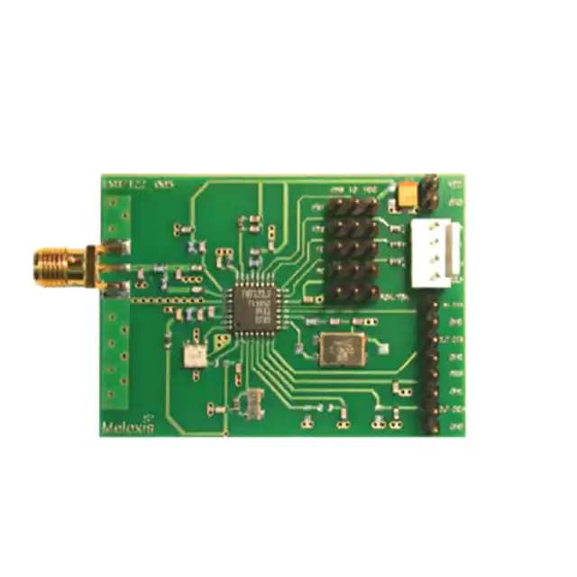
EVB comes with a cable to connect to a PC’s
LPT port
EVB programming software is available on
Melexis web site
Ordering Information
Part No.
EVB7122-315-FSK-C
EVB7122-433-FSK-C
EVB7122-868-FSK-C
EVB7122-915-FSK-C
* EVB7122-XXX-YYY-C with XXX = Reception frequency (315, 433.92, 868.3 or 915MHz) and YYY = Modulation (FSK or ASK).
** EVB default population is FSK, ASK modifications according to paragraph 4.2 and 4.3.
*** The evaluation board is supplied with a SMA connector.
Application Examples
Evaluation Board Example
General bi-directional half duplex digital data
RF signaling or analog signal communication
Tire Pressure Monitoring Systems (TPMS)
Remote Keyless Entry (RKE)
Low-power telemetry systems
Alarm and security systems
Wireless access control
Garage door openers
Networking solutions
Active RFID tags
Remote controls
Home and building automation
General Description
The TH7122 is a single chip FSK/FM/ASK transceiver IC. It is designed to operate in low-power multichannel programmable or single-channel stand-alone, half-duplex data transmission systems. It can be used
for applications in automotive, industrial-scientific-medical (ISM), short range devices (SRD) or similar
applications operating in the frequency range of 300 MHz to 930 MHz. In programmable user mode, the
transceiver can operate down to 27 MHz by employing an external VCO varactor diode.
39012 07122 02
Rev. 006
Page 1 of 24
EVB Description
June/08
�EVB7122
27 to 930MHz Transceiver
Evaluation Board Description
Document Content
1
2
Theory of Operation ...................................................................................................3
1.1
General ............................................................................................................................. 3
1.2
Technical Data Overview.................................................................................................. 3
1.3
Note on ASK Operation .................................................................................................... 3
1.4
Block Diagram .................................................................................................................. 4
1.5
User Mode Features ......................................................................................................... 4
Description of User Modes........................................................................................5
2.1
2.1.1
2.1.2
2.1.3
2.1.4
2.2
2.2.1
3
Frequency Selection .................................................................................................................... 5
Operation Mode ........................................................................................................................... 5
Modulation Type .......................................................................................................................... 6
LNA Gain Mode ........................................................................................................................... 6
Programmable User Mode Operation............................................................................... 6
Serial Control Interface Description ............................................................................................. 6
Register Description ..................................................................................................7
3.1
3.1.1
3.1.2
3.1.3
3.1.4
3.1.5
4
Stand-alone User Mode Operation ................................................................................... 5
Register Overview ............................................................................................................ 8
Default Register Settings for FS0, FS1........................................................................................ 8
A – word ....................................................................................................................................... 9
B – word ..................................................................................................................................... 10
C – word..................................................................................................................................... 11
D – word..................................................................................................................................... 12
Application Circuits .................................................................................................13
4.1
4.1.1
4.1.2
4.2
4.2.1
4.2.2
4.3
4.3.1
4.3.2
FSK Application Circuit Programmable User Mode (internal AFC option)...................... 13
Board Component Values for FSK Reception ........................................................................... 14
Component Arrangement Top Side for FSK Reception ............................................................ 15
ASK Application Circuit Programmable User Mode (normal data slicer option) ............. 16
Board Component Values for ASK (normal data slicer option) ................................................. 17
Component Arrangement Top Side for ASK Reception (normal data slicer option) ................. 18
ASK Application Circuit with Peak Detector Option ........................................................ 19
Board Component Values for ASK (peak detector option)........................................................ 20
Component Arrangement Top Side for ASK Reception (peak detector option)........................ 21
5
Evaluation Board Layouts .......................................................................................22
6
Package Description ................................................................................................23
6.1
7
Soldering Information ..................................................................................................... 23
Disclaimer .................................................................................................................24
39012 07122 02
Rev. 006
Page 2 of 24
EVB Description
June/08
�EVB7122
27 to 930MHz Transceiver
Evaluation Board Description
1
Theory of Operation
1.1
General
The main building block of the transceiver is a programmable PLL frequency synthesizer that is based on an
integer-N topology. The PLL is used for generating the carrier frequency during transmission and for
generating the LO signal during reception. The carrier frequency can be FSK-modulated by pulling the
crystal and ASK-modulated by on/off keying of the power amplifier. The receiver is based on the principle of
a single conversion superhet. Therefore the VCO frequency has to be changed between transmit and
receive mode. In receive mode, the preferred LO injection type is low-side injection.
The TH7122 transceiver IC consists of the following building blocks:
1.2
Low-noise amplifier (LNA) for high-sensitivity
RF signal reception with switchable gain
Mixer (MIX) for RF-to-IF down-conversion
IF amplifier (IFA) to amplify and limit the IF
signal and for RSSI generation
Phase-coincidence demodulator with external
ceramic discriminator (FSK Demodulator)
Operational amplifier (OA1), connected to
demodulator output
Operational amplifier (OA2), for geral use
Peak detector (PKDET) for ASK detection
Control logic with 3wire bus serial control
interface (SCI)
Reference oscillator (RO) with external crystal
Reference divider (R counter)
Programmable divider (N/A counter)
Phase-frequency detector (PFD)
Charge pump (CP)
Voltage controlled oscillator (VCO) with internal
varactor
Power amplifier (PA) with adjustable output
power
Technical Data Overview
Frequency range: 300 MHz to 930 MHz in
programmable user mode
Extended frequency range with external VCO
varactor diode: 27 MHz to 930 MHz
315 MHz, 433 MHz, 868 MHz or 915 MHz fixedfrequency settings in stand-alone mode
Power supply range: 2.2 V to 5.5 V
Temperature range: -40 °C to +85 °C
Standby current: 50 nA
Operating current in receive: 6.5 mA (low gain)
Operating current in transmit: 12 mA (at -2 dBm)
Adjustable RF power range: -20 dBm to
+10dBm
Sensitivity: -105 dBm at FSK with 180 kHz
IF filter BW
1.3
Sensitivity: -107 dBm at ASK with 180 kHz
IF filter BW
Max. data rate with crystal pulling: 20 kbps NRZ
Max. data rate with direct VCO modulation:
115 kbps NRZ
Max. input level: -10 dBm at FSK
and -20 dBm at ASK
Input frequency acceptance: ± 10 to ± 150 kHz
(depending on FSK deviation)
FM/FSK deviation range: ±2.5 to ±80 kHz
Analog modulation frequency: max. 10 kHz
Crystal reference frequency: 3 MHz to 12 MHz
External reference frequency: 1 MHz to 16 MHz
Note on ASK Operation
Optimum ASK performance can be achieved by using an 8-MHz crystal for operation at 315 MHz, 434 MHz
and 915 MHz. For details please refer to the software settings shown in sections 4.2 and 4.3. FSK operation
is the preferred choice for applications in the European 868MHz band.
For more detailed information, please refer to the latest TH7122 data sheet revision
39012 07122 02
Rev. 006
Page 3 of 24
EVB Description
June/08
�EVB7122
27 to 930MHz Transceiver
Evaluation Board Description
2
7
3 IN_DEM
RSSI
1
VCC_IF
31
IN_IFA
32
VEE_IF
6 OUT_DEM
PKDET
SW1
1.5pF
26
FSK Demodulator
MIX
LNA
5
INT1
IFA
SW2
OA1
Control Logic
15
16
TE/SDTA
13
RE/SCLK
12
ASK/FSK
9
IN_DTA
19
VEE_RO
11
FS1/LD
22 VEE_PLL 10 RO
17
FS0/SDEN
FSK
FSK_SW
23 LF
SCLK
21 TNK_LO 20 VCC_PLL
Fig. 1:
1.5
RO
SDTA
RO
PA
24 PS_PA
SCI
R
counter
SDEN
N
counter
VCO
25
8
OUT_DTA
200k
LO
OUT_PA
4
INT2/PDO
MIX
IF
ASK
OA2
18
14
VCC_DIG
IN_LNA
bias
VEE_DIG
30
OUT_MIX
28
IN_MIX
29
OUT_LNA
27
GAIN_LNA
Block Diagram
VEE_LNA
1.4
TH7122 block diagram
User Mode Features
The transceiver can operate in two different user modes. It can be used either as a 3wire-bus-controlled
programmable or as a stand-alone fixed-frequency device. After power up, the transceiver is set to Standalone User Mode (SUM). In this mode, pins FS0/SDEN and FS1/LD must be connected to VEE or VCC in
order to set the desired frequency of operation. There are 4 pre-defined frequency settings: 315MHz,
433.92MHz, 868.3MHz and 915MHz. The logic level at pin FS0/SDEN must not be changed after power up
in order to remain in fixed-frequency mode.
After the first logic level change at pin FS0/SDEN, the transceiver enters into Programmable User Mode
(PUM). In this mode, the user can set any PLL frequency or mode of operation by the SCI. In SUM pins
FS0/SDEN and FS1/LD are used to set the desired frequency, while in PUM pin FS0/SDEN is part of the
3-wire serial control interface (SCI) and pin FS1/LD is the look detector output signal of the PLL synthesizer.
A mode control logic allows several operating modes. In addition to standby, transmit and receive mode, two
idle modes can be selected to run either the reference oscillator only or the whole PLL synthesizer. The PLL
settings for the PLL idle mode are taken over from the last operating mode which can be either receive or
transmit mode.
The different operating modes can be set in SUM and PUM as well. In SUM the user can program the
transceiver via control pins RE/SCLK and TE/SDTA. In PUM the register bits OPMODE are used to select
the modes of operation while pins RE/SCLK and TE/SDTA are part of the SCI.
39012 07122 02
Rev. 006
Page 4 of 24
EVB Description
June/08
�EVB7122
27 to 930MHz Transceiver
Evaluation Board Description
2
Description of User Modes
2.1
Stand-alone User Mode Operation
After power up the transceiver is set to stand-alone user mode. In this mode, pins FS0/SDEN and FS1/LD
must be connected to VEE or VCC to set the desired frequency of operation. The logic level at pin FS0/SDEN
must not be changed after power up in order to remain in stand-alone user mode. The default settings of the
control word bits in stand-alone user mode are described in the frequency selection table. Detailed
information about the default settings can be found in the tables of section 5.
2.1.1
Frequency Selection
Channel frequency
433.92 MHz
868.3 MHz
315 MHz
915 MHz
FS0/SDEN
1
0
1
0
FS1/LD
0
0
1
1
Reference oscillator frequency
R counter ratio in RX mode (RR)
7.1505 MHz
32
16
18
32
223.45 kHz
446.91 kHz
397.25 kHz
223.45 kHz
1894
1919
766
4047
VCO frequency in RX mode
423.22 MHz
857.60 MHz
304.30 MHz
904.30 MHz
RX frequency
433.92 MHz
868.30 MHz
315.00 MHz
915.00 MHz
32
16
18
32
223.45 kHz
446.91 kHz
397.25 kHz
223.45 kHz
1942
1943
793
4095
VCO frequency in TX mode
433.92 MHz
868.30 MHz
315.00 MHz
915.00 MHz
TX frequency
433.92 MHz
868.30 MHz
315.00 MHz
915.00 MHz
IF in RX mode
10.7 MHz
10.7 MHz
10.7 MHz
10.7 MHz
PFD frequency in RX mode
N counter ratio in RX mode (NR)
R counter ratio in TX mode (RT)
PFD frequency in TX mode
N counter ratio in TX mode (NT)
In stand-alone user mode, the transceiver can be set to Standby, Receive, Transmit or Idle mode (only PLL
synthesizer active) via control pins RE/SCLK and TE/SDTA. The modulation scheme and the LNA gain are
set by pins ASK/FSK and GAIN_LNA, respectively.
2.1.2
Operation Mode
Operation mode
Standby
Receive
Transmit
Idle
RE/SCLK
0
1
0
1
TE/SDTA
0
0
1
1
Note: Pins with internal pull-down
39012 07122 02
Rev. 006
Page 5 of 24
EVB Description
June/08
�EVB7122
27 to 930MHz Transceiver
Evaluation Board Description
2.1.3
2.1.4
2.2
Modulation Type
Modulation type
ASK
FSK
ASK / FSK
0
1
LNA gain
high
low
GAIN_LNA
0
1
LNA Gain Mode
Programmable User Mode Operation
The transceiver can also be used in programmable user mode. After power-up the first logic change at pin
FS0/SDEN enters into this mode. Now full programmability can be achieved via the Serial Control Interface
(SCI).
2.2.1
Serial Control Interface Description
A 3-wire (SCLK, SDTA, SDEN) Serial Control Interface (SCI) is used to program the transceiver in programmable user mode. At each rising edge of the SCLK signal, the logic value on the SDTA pin is written into a
24-bit shift register. The data stored in the shift register are loaded into one of the 4 appropriate latches on
the rising edge of SDEN. The control words are 24 bits lengths: 2 address bits and 22 data bits. The first two
bits (bit 23 and 22) are latch address bits. As additional leading bits are ignored, only the least significant 24
bits are serial-clocked into the shift register. The first incoming bit is the most significant bit (MSB). To
program the transceiver in multi-channel application, four 24-bit words may be sent: A-word, B-word, C-word
and D-word. If individual bits within a word have to be changed, then it is sufficient to program only the
appropriate 24-bit word. The serial data input timing and the structure of the control words are illustrated in
Fig. 2 and 3.
SDTA
SCLK
24-BIT
SHIFT REGISTER
22
22
22
2
22
‘00’
SDEN
ADDR DECODER
Fig. 2:
39012 07122 02
Rev. 006
‘01’
‘10’
‘11’
22
A - LATCH
22
A-word
B - LATCH
22
B-word
C - LATCH
22
C-word
D - LATCH
22
D-word
SCI Block Diagram
Page 6 of 24
EVB Description
June/08
�EVB7122
27 to 930MHz Transceiver
Evaluation Board Description
Due to the static CMOS design, the SCI consumes virtually no current and it can be programmed in active
as well as in standby mode.
If the transceiver is set from standby mode to any of the active modes (idle, receive, transmit), the SCI
settings remain the same as previously set in one of the active modes, unless new settings are done on the
SCI while entering into an active mode.
Invalid
data
SDTA
MSB
bit 23
LSB
bit 22
bit 1
t CH
t CWL tCWH
Invalid
data
bit 0
SCLK
SDEN
t CS
tES
Fig. 3:
3
tEW
tEH
Serial Data Input Timing
Register Description
As shown in the previous section there are four control words which stipulate the operation of the whole chip.
In Stand-alone User Mode SUM the intrinsic default values with respect to the applied levels at pins FS0 and
FS1 lay down the configuration of the transceiver. In Programmable User Mode (PUM) the register settings
can be changed via 3-wire interface SCI. The default settings which vary with the desired operating
frequency depend on the voltage levels at the frequency selection pins FS0 and FS1 before entering the
PUM. Table 5.1.1 shows the default register settings of different frequency selections. It should be noted that
the channel frequency listed below will be achieved with a crystal frequency of 7.1505 MHz. The following
table depicts an overview of the register configuration of the TH7122.
39012 07122 02
Rev. 006
Page 7 of 24
EVB Description
June/08
�EVB7122
27 to 930MHz Transceiver
Evaluation Board Description
3.1
Register Overview
DATA
WORD
MSB
LSB
PACTRL
1
1
1
0
0
1
0
0
LNAHYST
AFC
OA2
1
1
1
0
1
0
3.1.1
4
3
2
1
Bit No.
Depends on FS0/FS1 voltage level after power up
default
9
8
7
6
5
4
3
2
1
0
Bit No.
Depends on FS0/FS1 voltage level after power up
default
9
8
7
6
5
4
3
2
1
0
0
Bit No.
NR
[ 16 : 0 ]
default
9
8
7
6
5
4
3
2
1
Depends on FS0/FS1 voltage level after power up
0
0
Bit No.
default
NT
[ 16 : 0 ]
1
ERTM
[ 1 :0 ]
0
LDTM
[ 1 :0 ]
D
0
MODCTRL
1
5
Depends on FS0/FS1 voltage level after power up
23 22 21 20 19 18 17 16 15 14 13 12 11 10
1
0
BAND
0
VCOCUR
[ 1 :0 ]
C
0
PFDPOL
0
LNACTRL
23 22 21 20 19 18 17 16 15 14 13 12 11 10
1
6
ROMIN
[2:0]
1
ROMAX
[2:0]
1
DELPLL
B
0
Set to 1
1
PKDET
23 22 21 20 19 18 17 16 15 14 13 12 11 10
0
7
RR
[9:0]
LOCKMODE
1
8
RT
[9:0]
1
9
OPMODE
[1:0]
0
LNAGAIN
0
Set to 1
0
TXPOWER
[ 1 :0 ]
0
CPCUR
A
0
MODSEL
0
DATAPOL
0
IDLE
23 22 21 20 19 18 17 16 15 14 13 12 11 10
Default Register Settings for FS0, FS1
FS1
FS0
Channel
frequency
BAND
VCOCUR
[1:0]
RR
[9:0]
NR
[ 16 :0 ]
RT
[ 9 :0 ]
NT
[ 16 : 0 ]
0
0
868.30 MHz
1
11
16d
1919d
16d
1943d
0
1
433.92 MHz
0
01
32d
1894d
32d
1942d
1
0
915.00 MHz
1
11
32d
4047d
32d
4095d
1
1
315.00 MHz
0
00
18d
766d
18d
793d
Note:
d – decimal code
A detailed description of the registers function and their configuration can be found in the following sections.
39012 07122 02
Rev. 006
Page 8 of 24
EVB Description
June/08
�EVB7122
27 to 930MHz Transceiver
Evaluation Board Description
3.1.2
A – word
Name
Bits
RR
[9:0]
Description
Reference divider ratio in RX operation mode
4d .. 1023d
Operation mode
OPMODE
[11:10]
00
01
10
11
Standby mode
Receive mode
Transmit mode
Idle mode
0
1
low LNA gain
high LNA gain
#default
LNA gain
LNAGAIN
[12]
#default
This selection is valid if bit LNACTR (bit 21 in C-word) is set to internal LNA gain control.
not used
[13]
set to ‘1’ for correct function
Output power steps
TXPOWER
[15:14]
00
01
10
11
P1
P2
P3
P4
#default
Set the PA-on condition
PACTRL
LOCKMODE
[16]
0
1
PA is switched on if the PLL locks
PA is always on in TX mode
Set the PLL locked state observation mode
#default
0
before lock only
#default
Locked state condition will be ascertained only one time afterwards the LD signal remains in
high state.
[17]
1
before and after lock
locked state will be observed permanently
Charge Pump output current
CPCUR
[18]
0
1
#default
260 µA
1300 µA
Modulation mode
MODSEL
[19]
0
1
#default
ASK
FSK
This selection is valid if bit MODCTRL (bit 21 in D-word) is set to internal modulation
control.
Input data polarity
0
DTAPOL
[20]
#default
normal
‘0’ for space at ASK or fmin at FSK, ‘1’ for mark at ASK or fmax at FSK
1
inverse
‘1’ for space at ASK or fmin at FSK, ‘0’ for mark at ASK or fmax at FSK
Active blocks in IDLE mode
IDLESEL
39012 07122 02
Rev. 006
[21]
0
1
only RO active
whole PLL active
Page 9 of 24
#default
EVB Description
June/08
�EVB7122
27 to 930MHz Transceiver
Evaluation Board Description
3.1.3
B – word
Name
Bits
RT
[9:0]
Description
Reference divider ratio in TX operation mode
4d .. 1023d
Set the desired steady state current of the reference oscillator
ROMIN
[12:10]
000
001
010
011
100
101
110
111
0 μA
75 μA
150 μA #default
225 μA
300 μA
375 μA
450 μA
525 μA
The control circuitry regulates the current of the oscillator core
between the values ROMAX and ROMIN. As the regulation input
signal the amplitude on pin RO is used. If the ROMIN value is
sufficient to achieve an amplitude of about 400mV on pin RO the
current of the reference oscillator core will be set to ROMIN.
Otherwise the current will be permanently regulated between
ROMAX and ROMIN. If ROMIN and ROMAX are equal no
regulation of the oscillator current occurs. Please also note the
block description of the reference oscillator in para. 3.1.1
Set the start-up current of the reference oscillator
ROMAX
[15:13]
000
001
010
011
100
101
110
111
0 μA
75 μA
150 μA
225 μA
300 μA
375 μA
450 μA
525 μA #default
Set the start-up current of the reference oscillator core. Please
also note the description of the ROMIN register and the block
description of the reference oscillator which can be seen above.
OA2 operation
OA2
[16]
0
1
#default
disabled
enabled
OA2 can be enabled in FSK receive mode. OA2 is disabled in ASK mode receive.
Internal AFC feature
AFC
[17]
0
1
#default
disabled
enabled
Hysteresis on pin GAIN_LNA
LNAHYST
[18]
0
1
disabled
enabled - typical 340 mV (V0→1 = 1.56V, V1→0 = 1.22V)
#default
Delayed start of the PLL
DELPLL
[19]
PLL starts at the reference oscillator start-up
0
undelayed start
1
starts after 8 valid RO-cycles
#default
PLL starts after 8 valid RO-cycles before entering an active mode to ensure reliable oscillation
of the reference oscillator.
not used
[20]
set to ‘1’ for correct function
RSSI Peak Detector
0
PKDET
[21]
#default
disabled
The RSSI output signal directly feeds the data slicer setup by means of OA1.
1
enabled
In ASK receive mode the RSSI Peak Detector output is multiplexed to pin INT2/PDO.
39012 07122 02
Rev. 006
Page 10 of 24
EVB Description
June/08
�EVB7122
27 to 930MHz Transceiver
Evaluation Board Description
3.1.4
C – word
Name
Bits
NR
[16:0]
BAND
[17]
Description
Feedback divider ratio in RX operation mode
64d .. 131071d
0
1
Set the desired frequency range
recommended at fRF < 500 MHz
recommended at fRF > 500MHz
Some tail current sources are linked to this bit in order to save current for low frequency
operations.
VCO active current
VCOCUR
[19:18]
00
01
10
11
low current (300 µA)
standard current (500 µA)
high1 current (700 µA)
high2 current (900 µA)
Phase Detector polarity
0
PFDPOL
[20]
1
negative
#default
VCO
OUTPUT
FREQUENCY
positive
pos
neg
VCO INPUT VOLTAGE
LNA gain control mode
0
LNACTRL
external LNA gain control
#default
LNA gain will be set via pin GAIN_LNA.
[21]
1
internal LNA gain control
LNA gain will be set via bit LNAGAIN (bit 12 in A-word). Nevertheless pin GAIN_LNA must
be connected to either VCC or VEE.
39012 07122 02
Rev. 006
Page 11 of 24
EVB Description
June/08
�EVB7122
27 to 930MHz Transceiver
Evaluation Board Description
3.1.5
D – word
Name
Bits
NT
[16:0]
Description
Feedback divider ratio in TX operation mode
64d .. 131071d
Set the unlock condition of the PLL
ERTM
[18:17]
00
01
10
11
2 clocks #default
4 clocks
8 clocks
16 clocks
Set the maximum allowed number of reference clocks
(1/fRO) during the phase detector output signals (UP & DOWN)
can be in-consecutive.
Set the lock condition of the PLL
LDTM
[20:19]
00
01
10
11
4 clocks
16 clocks #default
64 clocks
256 clocks
0
external modulation control
Set the minimum number of consecutive edges of phase
detector output cycles, without appearance of any unlock
condition.
Set mode of modulation control:
MODCTRL
#default
Modulation will be set via pin ASK/FSK.
[21]
1
internal modulation control
Modulation will be set via bit MODSEL (bit 19 in A-word). Nevertheless pin ASK/FSK must be
connected to either VCC or VEE.
39012 07122 02
Rev. 006
Page 12 of 24
EVB Description
June/08
�EVB7122
27 to 930MHz Transceiver
Evaluation Board Description
RSSI
GND
OUT_DEM
GND
FSK Application Circuit Programmable User Mode (internal AFC option)
IN_DTA
GND
OUT_DTA
GND
4.1
GND
SDTA
SDEN
SCLK
Application Circuits
VCC
GND
4
2 1
4 3 2 1
4 3 2 1
4 3 2 1
RS2
RS3
12 3
XTAL
9
VEE_RO
IN_DTA 12
FSK_SW 11
ASK/FSK 13
VCC_DIG 14
RO 10
INT2/PDO 4
CTX0
LRX2
CRX0
CTX1
CTX2
LTX1
31 VEE_IF
RP
CB5
IN_IFA 1
32 OUT_MIX
30 IN_MIX
29 GAIN_LNA
28 OUT_LNA
27 VEE_LNA
26 IN_LNA
VCC_IF 2
25 OUT_PA
23 LF
LTX0
C4
C3
C2
CERDIS
RL0
CERFIL
CB4
C1
L1
CB1
RB1
VCC
VCC
TH7122
IN_DEM 3
CTX4
50
INT1 5
22 VEE_PLL
24
CPS
OUT_DEM 6
21 TNK_LO
RPS
C5
RSSI 7
20 VCC_PLL
RF
CF1
39012 07122 02
Rev. 006
OUT_DTA 8
19 FS1/LD
L0
CB2
LX
18 VEE_DIG
CB6
C0
CF2
RE/SCLK 15
16
CB7
FS0/SDEN
17
CX1
CX2
ASK/FSK
12 3
RE/SCLK
12 3
TE/SDTA
RS1
12 3
FS0/SDEN
12 3
FS1/LD
CB0
TX_OUT
RX_IN
Page 13 of 24
EVB Description
June/08
�EVB7122
27 to 930MHz Transceiver
Evaluation Board Description
4.1.1
Board Component Values for FSK Reception
Part
Size
Value @
315 MHz
Value @
433.92
MHz
Value @
868.3 MHz
Value @
915 MHz
Tol.
C0
0603
1.2 pF
1.5 pF
1.8 pF
0.82 pF
±5%
VCO tank capacitor
C1
0603
3.9 pF
5.6 pF
2.2 pF
1.8 pF
±5%
LNA output tank capacitor
C2
0603
1.5 pF
1.5 pF
1.5 pF
1.5 pF
±5%
MIX input matching capacitor
C3
0603
10 nF
10 nF
10 nF
10 nF
±10%
data slicer capacitor
C4
0603
330 pF
330 pF
330 pF
330 pF
±5%
demodulator output low-pass
capacitor, depending on data rate
Description
C5
0603
1.5 nF
1.5 nF
1.5 nF
1.5 nF
±10%
RSSI output low pass capacitor
CB0
1210
10 μF
10 μF
10 μF
10 μF
±20%
de-coupling capacitor
CB1
0603
10 nF
10 nF
10 nF
10 nF
±10%
de-coupling capacitor
CB2
0603
330 pF
330 pF
330 pF
330 pF
±10%
de-coupling capacitor
CB4
0603
10 nF
10 nF
10 nF
10 nF
±10%
de-coupling capacitor
CB5
0603
100 nF
100 nF
100 nF
100 nF
±10%
de-coupling capacitor
CB6
0603
100 pF
100 pF
100 pF
100 pF
±10%
de-coupling capacitor
CB7
0603
100 nF
100 nF
100 nF
100 nF
±10%
de-coupling capacitor
CF1
0603
1 nF
1 nF
1 nF
1 nF
±10%
loop filter capacitor
CF2
0603
68 pF
120 pF
150 pF
82 pF
±5%
loop filter capacitor
CPS
0603
10 nF
10 nF
10 nF
10 nF
±10%
power-select capacitor
CX1
0603
8.2 pF
10 pF
12 pF
12 pF
±5%
RO capacitor for FSK (Δf = ±20 kHz)
CX2
0603
150 pF
56 pF
18 pF
15 pF
±5%
RO capacitor for FSK (Δf = ±20 kHz)
CRX0
0603
100 pF
100 pF
100 pF
100 pF
±5%
RX coupling capacitor
CTX0
0603
10 pF
10 pF
10 pF
10 pF
±5%
TX coupling capacitor
CTX1
0603
10 pF
6.8 pF
5.6 pF
4.7 pF
±5%
TX impedance matching capacitor
CTX2
0603
10 pF
6.8 pF
3.9 pF
3.9 pF
±5%
TX impedance matching capacitor
CTX4
0603
12 pF
4.7 pF
2.2 pF
1.8 pF
±5%
TX impedance matching capacitor
RB1
0603
100 Ω
100 Ω
100 Ω
100 Ω
±5%
protection resistor
RF
0603
47 kΩ
47 kΩ
33 kΩ
33 kΩ
±5%
loop filter resistor
RP
0603
3.3 kΩ
3.3 kΩ
3.3 kΩ
3.3 kΩ
±5%
CERDIS loading resistor
RL0
0603
390 Ω
390 Ω
390 Ω
390 Ω
±5%
CERFIL loading, optionally
RPS
0603
22 kΩ
33 kΩ
47 kΩ
47 kΩ
±5%
power-select resistor
RS1...RS3
0603
10 kΩ
10 kΩ
10 kΩ
10 kΩ
±5%
protection resistor
L0
0603
47 nH
22 nH
3.9 nH
3.9 nH
±5%
VCO tank inductor
from Würth-Elektronik (WE-KI series)
or equivalent part
L1
0603
33 nH
15 nH
4.7 nH
4.7 nH
±5%
LNA output tank inductor
from Würth-Elektronik (WE-KI series)
or equivalent part
LRX2
0603
82 nH
56 nH
15 nH
15 nH
±5%
LTX0
0603
15 nH
15 nH
3.9 nH
3.9 nH
±5%
LTX1
0603
33 nH
33 nH
10 nH
10 nH
±5%
LX
0603
0Ω
0Ω
10 nH
10 nH
±5%
XTAL
HC49
SMD
7x5
7.1505 MHz
±20ppm cal., ±20ppm temp.
CERFIL
SMD
3.45x3.1
SFECF10M7HA00
B3dB = 180 kHz
CERDIS
SMD
4.5x2
CDSCB10M7GA136
39012 07122 02
Rev. 006
Page 14 of 24
impedance matching inductor
from Würth-Elektronik (WE-KI series)
or equivalent part
RO inductor
fundamental-mode crystal from:
Telcona/Hong Kong X’tals
C5L7150500D10F3EHK02
ceramic filter from Murata,
or equivalent part
ceramic Discriminator from Murata,
or equivalent part
EVB Description
June/08
�EVB7122
27 to 930MHz Transceiver
Evaluation Board Description
GND
OUT DEM
GND
RSSI
XTAL
CX2
C3
CB7
LX
1
RE
TE
FS0
C4
3
C5
CX1
GND LD VCC
CB0
FS1
GND
OUT DTA
GND
IN DTA
SDEN
RS3
ASK/FSK
SDTA
RS2
SCLK
GND
RS1
GND
Component Arrangement Top Side for FSK Reception
VCC
4.1.2
L0
C0
CF2
CF1
CB6
CERDIS
RF
CB5
RP
CB4
RPS
CPS
CTX0
CB2
LTX0
CRX0
C2
CTX4
RB1
LRX2
Melexis
LTX1
EVB7122_005
L1
CB1
CTX1
RX_input
CTX2
TX_output
39012 07122 02
Rev. 006
C1
Board size is 39.5mm x 56.5mm
Page 15 of 24
EVB Description
June/08
�EVB7122
27 to 930MHz Transceiver
Evaluation Board Description
GND
SDTA
SDEN
SCLK
IN_DTA
GND
OUT_DTA
GND
RSSI
GND
OUT_DEM
GND
ASK Application Circuit Programmable User Mode (normal data slicer option)
VCC
GND
2 1
4 3 2 1
4 3 2 1
4 3 2 1
12 3
12 3
RE/SCLK
TE/SDTA
ASK/FSK
RS2
RS3
RS1
12 3
FS0/SDEN
12 3
FS1/LD
CB0
12 3
4.2
CX1
XTAL
LRX2
CTX1
CTX2
9
VEE_RO
RO 10
FSK_SW 11
IN_DTA 12
RL0
C2
CERFIL
C1
CB1
L1
LTX1
IN_IFA 1
32 OUT_MIX
31 VEE_IF
30 IN_MIX
29 GAIN_LNA
28 OUT_LNA
26 IN_LNA
CRX0
CB5
RB1
VCC
CTX0
LTX0
27 VEE_LNA
VCC_IF 2
25 OUT_PA
IN_DEM 3
23 LF
CTX4
C3
INT2/PDO 4
22 VEE_PLL
24
CPS
INT1 5
TH7122
21 TNK_LO
RPS
VCC
ASK/FSK 13
OUT_DEM 6
20 VCC_PLL
RF
CF1
C5
RSSI 7
19 FS1/LD
L0
CB2
OUT_DTA 8
18 VEE_DIG
CB6
C0
CF2
VCC_DIG 14
16
FS0/SDEN
17
RE/SCLK 15
CB7
TX_OUT
RX_IN
50
Software Settings for ASK
fRO = 8.0000MHz
CPCUR
VCOCUR
Channel
frequency
RR
NR
RT
NT
RX
TX
RX
TX
315.00 MHz
80
3043
8
315
260µA
1300µA
300µA
900µA
434.00 MHz
80
4233
8
434
260µA
1300µA
300µA
900µA
915.00 MHz
80
9043
8
915
260µA
1300µA
300µA
900µA
39012 07122 02
Rev. 006
Page 16 of 24
EVB Description
June/08
�EVB7122
27 to 930MHz Transceiver
Evaluation Board Description
4.2.1
Board Component Values for ASK (normal data slicer option)
Part
Size
Value @
315 MHz
Value @
434 MHz
Value @
915 MHz
Tol.
C0
0603
1.5 pF
C1
0603
3.9 pF
1.8 pF
1 pF
±5%
VCO tank capacitor
5.6 pF
1.8 pF
±5%
C2
0603
LNA output tank capacitor
1.5 pF
1.0 pF
1.5 pF
±5%
C3
MIX input matching capacitor
0603
10 nF
10 nF
10 nF
±10%
C5
data slicer capacitor
0603
1.5 nF
1.5 nF
1.5 nF
±10%
RSSI output low pass capacitor
CB0
1210
10 μF
10 μF
10 μF
±20%
de-coupling capacitor
CB1
0603
10 nF
10 nF
10 nF
±10%
de-coupling capacitor
CB2
0603
330 pF
330 pF
330 pF
±10%
de-coupling capacitor
CB5
0603
100 nF
100 nF
100 nF
±10%
de-coupling capacitor
CB6
0603
100 pF
100 pF
100 pF
±10%
de-coupling capacitor
CB7
0603
100 nF
100 nF
100 nF
±10%
de-coupling capacitor
CF1
0603
100 pF
100 pF
100 pF
±10%
loop filter capacitor
CF2
0603
39 pF
39 pF
39 pF
±5%
loop filter capacitor
CPS
0603
1 nF
1 nF
1 nF
±10%
power-select capacitor,
depending ondata rate
RO capacitor
Description
CX1
0603
18 pF
18 pF
18 pF
±5%
CRX0
0603
100 pF
100 pF
10 pF
±5%
RX coupling capacitor
CTX0
0603
10 pF
10 pF
10 pF
±5%
TX coupling capacitor
CTX1
0603
10 pF
6.8 pF
4.7 pF
±5%
TX impedance matching capacitor
CTX2
0603
10 pF
6.8 pF
3.9 pF
±5%
TX impedance matching capacitor
CTX4
0603
12 pF
4.7 pF
1.8 pF
±5%
TX impedance matching capacitor
RB1
0603
100 Ω
100 Ω
100 Ω
±5%
protection resistor
RF
0603
33 kΩ
33 kΩ
33 kΩ
±5%
loop filter resistor
RP
0603
3.3 KΩ
3.3 KΩ
3.3 KΩ
±5%
CERDIS loading resistor
RL0
0603
390 Ω
390 Ω
390 Ω
±5%
CERFIL loading, optionally
RPS
0603
18 kΩ
33 kΩ
43 kΩ
±5%
power-select resistor
RS1...RS3
0603
10 kΩ
10 kΩ
10 kΩ
±5%
protection resistor
L0
0603
47 nH
27 nH
3.9 nH
±5%
VCO tank inductor
from Würth-Elektronik (WE-KI series)
or equivalent part
L1
0603
33 nH
15 nH
4.7 nH
±5%
LNA output tank inductor
from Würth-Elektronik (WE-KI series)
or equivalent part
LRX2
0603
82 nH
56 nH
15 nH
±5%
LTX0
0603
15 nH
15 nH
3.9 nH
±5%
LTX1
0603
33 nH
33 nH
10 nH
±5%
XTAL
HC49
SMD
7x5
8.0000 MHz
±20ppm cal., ±20ppm temp.
CERFIL
SMD
3.45x3.1
SFECF10M7HA00
B3dB = 180 kHz
39012 07122 02
Rev. 006
Page 17 of 24
impedance matching inductor
from Würth-Elektronik (WE-KI series)
or equivalent part
fundamental-mode crystal from:
Telcona/Hong Kong X’tals
C5L8000000D10F3EHK01
ceramic filter from Murata,
or equivalent part
EVB Description
June/08
�EVB7122
27 to 930MHz Transceiver
Evaluation Board Description
GND
OUT DEM
C3
CB7
1
RE
TE
FS0
FS1
XTAL
3
C5
CX1
GND LD VCC
CB0
GND
RSSI
GND
OUT DTA
GND
IN DTA
SDEN
RS3
ASK/FSK
SDTA
RS2
SCLK
GND
RS1
GND
Component Arrangement Top Side for ASK Reception (normal data slicer option)
VCC
4.2.2
L0
C0
CF2
CF1
CB6
RF
CB5
RPS
CPS
CTX0
CB2
LTX0
CRX0
C2
CTX4
RB1
LRX2
Melexis
LTX1
EVB7122_005
L1
CB1
CTX1
RX_input
CTX2
TX_output
39012 07122 02
Rev. 006
C1
Board size is 39.5mm x 56.5mm
Page 18 of 24
EVB Description
June/08
�EVB7122
27 to 930MHz Transceiver
Evaluation Board Description
GND
SDTA
SDEN
SCLK
IN_DTA
GND
OUT_DTA
GND
RSSI
GND
OUT_DEM
GND
ASK Application Circuit with Peak Detector Option
VCC
GND
2 1
4 3 2 1
4 3 2 1
4 3 2 1
12 3
12 3
RE/SCLK
TE/SDTA
ASK/FSK
RS2
RS3
RS1
12 3
FS0/SDEN
12 3
FS1/LD
CB0
12 3
4.3
CX1
XTAL
LRX2
CRX0
CTX2
9
VEE_RO
RO 10
FSK_SW 11
ASK/FSK 13
IN_DTA 12
32 OUT_MIX
31 VEE_IF
30 IN_MIX
29 GAIN_LNA
C6
CB5
IN_IFA 1
RL0
C2
CERFIL
C1
CB1
L1
LTX1
R1
RB1
VCC
CTX0
LTX0
26 IN_LNA
CTX4
28 OUT_LNA
VCC_IF 2
27 VEE_LNA
23 LF
25 OUT_PA
IN_DEM 3
CTX1
VCC
INT2/PDO 4
22 VEE_PLL
24
R2
INT1 5
TH7122
21 TNK_LO
RPS
CPS
OUT_DEM 6
20 VCC_PLL
RF
CF1
C5
RSSI 7
19 FS1/LD
L0
CB2
OUT_DTA 8
18 VEE_DIG
CB6
C0
CF2
VCC_DIG 14
16
FS0/SDEN
17
RE/SCLK 15
CB7
TX_OUT
RX_IN
50
Software Settings for ASK
fRO = 8.0000MHz
CPCUR
VCOCUR
Channel
frequency
RR
NR
RT
NT
RX
TX
RX
TX
315.00 MHz
80
3043
8
315
260µA
1300µA
300 µA
900µA
434.00 MHz
80
4233
8
434
260µA
1300µA
300 µA
900µA
915.00 MHz
80
9043
8
915
260µA
1300µA
300 µA
900µA
39012 07122 02
Rev. 006
Page 19 of 24
EVB Description
June/08
�EVB7122
27 to 930MHz Transceiver
Evaluation Board Description
4.3.1
Board Component Values for ASK (peak detector option)
Part
Size
Value @
315 MHz
Value @
434 MHz
Value @
915 MHz
Tol.
C0
0603
1.8 pF
C1
0603
3.9 pF
2.2 pF
1 pF
±5%
VCO tank capacitor
5.6 pF
1.8 pF
±5%
C2
0603
LNA output tank capacitor
1.5 pF
1.0 pF
1.5 pF
±5%
C5
MIX input matching capacitor
0603
1.5 nF
1.5 nF
1.5 nF
±10%
C6
RSSI output low pass capacitor
0603
100 nF
100 nF
100 nF
±10%
PKDET capacitor
CB0
1210
10 μF
10 μF
10 μF
±20%
de-coupling capacitor
CB1
0603
10 nF
10 nF
10 nF
±10%
de-coupling capacitor
CB2
0603
330 pF
330 pF
330 pF
±10%
de-coupling capacitor
CB5
0603
100 nF
100 nF
100 nF
±10%
de-coupling capacitor
CB6
0603
100 pF
100 pF
100 pF
±10%
de-coupling capacitor
CB7
0603
100 nF
100 nF
100 nF
±10%
de-coupling capacitor
CF1
0603
100 pF
100 pF
100 pF
±10%
loop filter capacitor
CF2
0603
39 pF
39 pF
39 pF
±5%
loop filter capacitor
CPS
0603
1 nF
1 nF
1 nF
±10%
power-select capacitor,
depending on data rate
RO capacitor
Description
CX1
0805
18 pF
18 pF
18 pF
±5%
CRX0
0603
100 pF
100 pF
10 pF
±5%
RX coupling capacitor
CTX0
0603
10 pF
10 pF
10 pF
±5%
TX coupling capacitor
CTX1
0603
10 pF
6.8 pF
4.7 pF
±5%
TX impedance matching capacitor
CTX2
0603
10 pF
6.8 pF
3.9 pF
±5%
TX impedance matching capacitor
CTX4
0603
12 pF
4.7 pF
1.8 pF
±5%
TX impedance matching capacitor
R1
0603
100 kΩ
100 kΩ
100 kΩ
±5%
PKDET resistor
R2
0603
680 kΩ
680 kΩ
680 kΩ
±5%
PKDET resistor
RB1
0603
100 Ω
100 Ω
100 Ω
±5%
protection resistor
RF
0603
33 kΩ
33 kΩ
33 kΩ
±5%
loop filter resistor
RP
0603
3.3 KΩ
3.3 KΩ
3.3 KΩ
±5%
CERDIS loading resistor
RL0
0603
390 Ω
390 Ω
390 Ω
±5%
CERFIL loading, optionally
RPS
0603
18 kΩ
33 kΩ
43 kΩ
±5%
power-select resistor
RS1...RS3
0603
10 kΩ
10 kΩ
10 kΩ
±5%
protection resistor
L0
0603
47 nH
27 nH
3.9 nH
±5%
VCO tank inductor
from Würth-Elektronik (WE-KI series)
or equivalent part
L1
0603
33 nH
15 nH
4.7 nH
±5%
LNA output tank inductor
from Würth-Elektronik (WE-KI series)
or equivalent part
LRX2
0603
82 nH
56 nH
15 nH
±5%
LTX0
0603
15 nH
15 nH
3.9 nH
±5%
LTX1
0603
33 nH
33 nH
10 nH
±5%
XTAL
HC49
SMD
7x5
8.0000 MHz
±20ppm cal., ±20ppm temp.
CERFIL
SMD
3.45x3.1
SFECF10M7HA00
B3dB = 180 kHz
39012 07122 02
Rev. 006
Page 20 of 24
impedance matching inductor
from Würth-Elektronik (WE-KI series)
or equivalent part
fundamental-mode crystal from:
Telcona/Hong Kong X’tals
C5L8000000D10F3EHK01
ceramic filter from Murata,
or equivalent part
EVB Description
June/08
�EVB7122
27 to 930MHz Transceiver
Evaluation Board Description
GND
OUT DEM
R1
R2
CB7
1
RE
TE
FS0
FS1
XTAL
3
C5
CX1
GND LD VCC
CB0
GND
RSSI
GND
OUT DTA
GND
IN DTA
SDEN
RS3
ASK/FSK
SDTA
RS2
SCLK
GND
RS1
GND
Component Arrangement Top Side for ASK Reception (peak detector option)
VCC
4.3.2
C6
L0
C0
CF2
CF1
CB6
RF
CB5
RPS
CPS
CTX0
CB2
LTX0
CRX0
C2
CTX4
RB1
LRX2
Melexis
LTX1
EVB7122_005
L1
CB1
CTX1
RX_input
CTX2
TX_output
39012 07122 02
Rev. 006
C1
Board size is 39.5mm x 56.5mm
Page 21 of 24
EVB Description
June/08
�EVB7122
27 to 930MHz Transceiver
Evaluation Board Description
Evaluation Board Layouts
GND
OUT DEM
GND
GND
RSSI
OUT DTA
GND
ASK/FSK
IN DTA
SCLK
SDTA
GND
Board layout data in Gerber format is available, board size is 39.5mm x 56.5mm.
Melexis
RE
TE
FS0
EVB7122_005
FS1
GND LD VCC
VCC
GND
•
SDEN
5
PCB bottom view
PCB top view
39012 07122 02
Rev. 006
Page 22 of 24
EVB Description
June/08
�EVB7122
27 to 930MHz Transceiver
Evaluation Board Description
6
Package Description
The device TH7122 is RoHS compliant.
D
D1
A
24
17
16
25
E
b
e
E1
32
9
1
8
A2
A1
12° +1°
0.25
(0.0098)
c
L
12° +1°
Fig. 4:
.10 (.004)
LQFP32 (Low profile Quad Flat Package)
All Dimension in mm, coplanaríty < 0.1mm
E1, D1
E, D
A
A1
A2
e
b
c
L
α
7.00
9.00
1.40
1.60
0.05
0.15
1.35
1.45
0.8
0.30
0.45
0.09
0.20
0.45
0.75
0°
7°
0.053
0.057
0.031
0.012
0.018
0.0035
0.0079
0.018
0.030
0°
7°
min
max
All Dimension in inch, coplanaríty < 0.004”
min
max
6.1
0.276
0.354
0.055
0.063
0.002
0.006
Soldering Information
•
39012 07122 02
Rev. 006
The device TH7122 is qualified for MSL3 with soldering peak temperature 260 deg C
according to JEDEC J-STD-20
Page 23 of 24
EVB Description
June/08
�EVB7122
27 to 930MHz Transceiver
Evaluation Board Description
7
Disclaimer
1) The information included in this documentation is subject to Melexis intellectual and other property
rights. Reproduction of information is permissible only if the information will not be altered and is accompanied by all associated conditions, limitations and notices.
2) Any use of the documentation without the prior written consent of Melexis other than the one set forth in
clause 1 is an unfair and deceptive business practice. Melexis is not responsible or liable for such altered documentation.
3) The information furnished by Melexis in this documentation is provided ’as is’. Except as expressly warranted in any other applicable license agreement, Melexis disclaims all warranties either express, implied, statutory or otherwise including but not limited to the merchantability, fitness for a particular purpose, title and non-infringement with regard to the content of this documentation.
4) Notwithstanding the fact that Melexis endeavors to take care of the concept and content of this documentation, it may include technical or factual inaccuracies or typographical errors. Melexis disclaims any
responsibility in connection herewith.
5) Melexis reserves the right to change the documentation, the specifications and prices at any time and
without notice. Therefore, prior to designing this product into a system, it is necessary to check with
Melexis for current information.
6) Melexis shall not be liable to recipient or any third party for any damages, including but not limited to
personal injury, property damage, loss of profits, loss of use, interrupt of business or indirect, special incidental or consequential damages, of any kind, in connection with or arising out of the furnishing, performance or use of the information in this documentation.
7) The product described in this documentation is intended for use in normal commercial applications. Applications requiring operation beyond ranges specified in this documentation, unusual environmental requirements, or high reliability applications, such as military, medical life-support or life-sustaining equipment are specifically not recommended without additional processing by Melexis for each application.
8) Any supply of products by Melexis will be governed by the Melexis Terms of Sale, published on
www.melexis.com.
© Melexis NV. All rights reserved.
For the latest version of this document, go to our website at:
www.melexis.com
Or for additional information contact Melexis Direct:
Europe, Africa:
Americas:
Asia:
Phone: +32 1367 0495
E-mail: sales_europe@melexis.com
Phone: +1 603 223 2362
E-mail: sales_usa@melexis.com
Phone: +32 1367 0495
E-mail: sales_asia@melexis.com
ISO/TS 16949 and ISO14001 Certified
39012 07122 02
Rev. 006
Page 24 of 24
EVB Description
June/08
�