MLX92212LSE-AAA-000-RE 数据手册
MLX92212LSE
3-Wire Hall Effect Latch / Switch
Features and Benefits
Application Examples
Low voltage supply : from 2.5V to 5.5V
Chopper-stabilized amplifier stage
Low power switch: 2.1mA
Wide temperature range: -40C to 150C
Automotive qualified: AEC-Q100
Optimized ESD performance: 8kV
Designed for standalone PCB applications
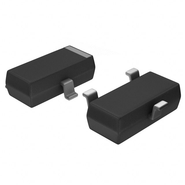
Thin SOT23 3L Green Compliant package
Automotive, Consumer and Industrial
BLDC motor commutation
Solid-state Latch
Low power applications
Index counting
Electrical power steering
Ordering Information
Product Code
Temperature Code
Package Code
Option code
Packing form code
MLX92212
L
SE
AAA-000
RE
MLX92212
L
SE
ABA-000
RE
MLX92212
L
SE
ACA-000
RE
Legend:
Temperature code:
Package Code:
Packing Form:
Ordering code
L (-40 to 150°C)
SE = TSOT-23L
RE = Reel
AAA = Very sensitive latch: Bop/Brp = 2mT/-2mT
ABA = Unipolar switch: Bop/Brp = 12.2mT/10.5mT
ACA = Unipolar switch: Bop/Brp = 10.1mT/8.3mT
Ordering Example: MLX92212LSE-AAA-000
1. Functional Diagram
VDD
Voltage
Regulator
VHALL
Regulator
Switched
Hall
Plate
Oscillator
2. General Description
Bandgap
Reference
BOP/BRP
Reference
OUT
Output Driver
Amplifier
Phase
generator
GND
POR
The Melexis MLX92212 is a low voltage Hall-effect switch
designed in mixed signal CMOS technology.
The device integrates a voltage regulator, Hall sensor with
advanced offset cancellation system and an open-drain
output driver, all in a single package.
The device features a low voltage regulator with
optimized
performances
targeting
low
power
consumption at low voltage levels.
It is suitable for use in automotive applications thanks to
its wide temperature range and extensive qualification
according to automotive standards.
The MLX92212 is delivered in a Green compliant 3-pin
Thin Small Outline Transistor (TSOT) for surface-mount
process.
REVISION 4 – November 2020
390109221203
Page 1 of 12
�MLX92212LSE
3-Wire Hall Effect Latch / Switch
Table of Contents
1. Functional Diagram .................................................................................................................................... 1
2. General Description .................................................................................................................................... 1
3. Glossary of Terms ........................................................................................................................................ 3
4. Absolute Maximum Ratings ..................................................................................................................... 3
5. General Electrical Specifications ............................................................................................................ 4
6. Magnetic Specification ............................................................................................................................... 5
6.1. MLX92212LSE-AAA-000-RE .......................................................................................................................... 5
6.2. MLX92212LSE-ABA-000-RE .......................................................................................................................... 5
6.3. MLX92212LSE-ACA-000-RE .......................................................................................................................... 5
7. Output behaviour versus Magnetic Field ............................................................................................ 6
7.1. Latch sensor: MLX92212LSE-AAA-000 .................................................................................................... 6
7.2. Switch sensor: MLX92212LSE-ABA-000, MLX92212LSE-ACA-000 ............................................... 6
8. Detailed General Description .................................................................................................................. 7
9. Latch/Switch characteristics ................................................................................................................... 7
10. Performance graphs................................................................................................................................. 8
10.1. MLX92212LSE -AAA-000 .............................................................................................................................. 8
10.2. MLX92212LSE -ABA-000 .............................................................................................................................. 8
11. Application Information ......................................................................................................................... 9
11.1. Typical Three-Wire Application Circuit .................................................................................................. 9
11.2. Automotive and Harsh, Noisy Environments Three-Wire Circuit ................................................ 9
12. Standard information regarding manufacturability of Melexis products with different
soldering processes ................................................................................................................................. 10
13. ESD Precautions...................................................................................................................................... 10
14. Package Information............................................................................................................................. 11
14.1. SE (TSOT-3L) Package Information ....................................................................................................... 11
15. Contact ....................................................................................................................................................... 12
16. Disclaimer ................................................................................................................................................. 12
REVISION 4 – November 2020
390109221203
Page 2 of 12
�MLX92212LSE
3-Wire Hall Effect Latch / Switch
3. Glossary of Terms
MilliTesla (mT), Gauss
RoHS
TSOT
ESD
BLDC
Units of magnetic flux density:
1mT = 10 Gauss
Restriction of Hazardous Substances
Thin Small Outline Transistor (TSOT package) – also referred with the Melexis
package code “SE”
Electro-Static Discharge
Brush-Less Direct-Current
4. Absolute Maximum Ratings
Parameter
Symbol
Value
Units
VDD
-0.5 to 6
V
IDD
± 20
mA
VOUT
-0.5 to 6
V
IOUT
± 20
mA
Operating Temperature Range
TA
-40 to 150
C
Storage Temperature Range
TS
-50 to 165
C
Maximum Junction Temperature
TJ
165
C
ESD Sensitivity – HBM
-
8000(2)
V
ESD Sensitivity – CDM
-
750
V
Supply Voltage
Supply Current
(1)
Output Voltage
Output Current
(1)
Table 1: Absolute maximum ratings
Note 1: Including current through the protection structure. Max Power dissipation should be also considered.
Note 2: Human Body Model according AEC-Q100-002 standard
Exceeding the absolute maximum ratings may cause permanent damage. Exposure to absolute-maximum-rated conditions for
extended periods may affect device reliability.
REVISION 4 – November 2020
390109221203
Page 3 of 12
�MLX92212LSE
3-Wire Hall Effect Latch / Switch
5. General Electrical Specifications
DC Operating Parameters TA = -40 to 150oC, VDD = 2.5V to 5.5V (unless otherwise specified)
Parameter
Symbol
Test Conditions
Min
Supply Voltage
VDD
Operating
2.5
Supply Current
IDD
Output Saturation Voltage
VDSON
IOUT = 5mA, B > BOP
Output Leakage Current
IOFF
B < BRP, VOUT = 5.5V
0.01
Output Rise Time (1)
tr
RL = 1k, CL = 50pF
0.25
s
Output Fall Time (1)
tf
RL = 1k, CL = 50pF
0.25
s
Power-On Time (2)
tPON
dVDD/dt > 2V/µs
Power-On Reset Voltage (3)
Power-On State
1.3
Typ
2.1
Max
Units
5.5
V
3.2
mA
0.5
V
10
A
38
70
s
VPOR
1.95
2.1
V
-
High
Maximum Switching
Frequency (1)
FSW
B≥±40mT and square
wave magnetic field
SE Package Thermal
Resistance
RTH
Single layer (1S) Jedec
board
10
KHz
300
°C/W
Table 2: Electrical specifications
1
Guaranteed by design and verified by characterization, not production tested
The Power-On time represents the time from reaching VDD = 2.5V to the first refresh of the output.
3
If VDD drops below VPOR the output is reset to High state.
2
REVISION 4 – November 2020
390109221203
Page 4 of 12
�MLX92212LSE
3-Wire Hall Effect Latch / Switch
6. Magnetic Specification
6.1. MLX92212LSE-AAA-000-RE
DC Operating Parameters TA = -40 upto 150 oC, VDD = 2.5V to 5.5V (unless otherwise specified)
Parameter
Operating Point
Release Point
Hysteresis
Symbol Test Conditions Min
BOP
BRP
BHYST
Typ
Max Units
TA = -40°C
0.6
2.1
3.8
mT
TA = 25°C
0.6
2.0
3.8
mT
TA = 150°C
0.6
1.9
3.8
mT
TA = -40°C
-3.8
-2.1
-0.6
mT
TA = 25°C
-3.8
-2.0
-0.6
mT
TA = 150°C
-3.8
-1.9
-0.6
mT
TA = -40°C
1.7
4.2
6.8
mT
TA = 25°C
1.7
4
6.8
mT
TA = 150°C
1.7
3.8
6.8
mT
6.2. MLX92212LSE-ABA-000-RE
DC Operating Parameters, TA = -40 upto 150 oC, VDD = 2.5V to 5.5V (unless otherwise specified)
Parameter
Symbol Test Conditions Min Typ
TA = -40°C
9.2 12.7
TA = 25°C
9.4 12.2
Operating Point
BOP
TA = 85°C
9.2 12.3
TA = 125°C
8.8 12.4
TA = 150°C
8.2 12.5
TA = -40°C
7.6
11
TA = 25°C
7.8 10.5
Release Point
BRP
TA = 85°C
7.8 10.6
TA = 125°C
7.4 10.7
TA = 150°C
6.8 10.8
Max Units
16.6 mT
15.4 mT
15.4 mT
16.0 mT
16.8 mT
14.4 mT
13.4 mT
13.4 mT
13.9 mT
14.8 mT
6.3. MLX92212LSE-ACA-000-RE
DC Operating Parameters, TA = -40 upto 150 oC, VDD = 2.5V to 5.5V (unless otherwise specified)
Parameter
Operating Point
Release Point
Symbol Test Conditions Min Typ Max Units
TA = -40°C
7.8 11.5 15.1 mT
BOP
BRP
REVISION 4 – November 2020
390109221203
TA = 25°C
6.9
10.1 13.3
mT
TA = 150°C
TA = -40°C
5.3
5.9
7.6
9.3
9.9
12.7
mT
mT
TA = 25°C
5.3
8.3
11.3
mT
TA = 150°C
4.2
6.6
9.0
mT
Page 5 of 12
�MLX92212LSE
3-Wire Hall Effect Latch / Switch
7. Output behaviour versus Magnetic Field
7.1. Latch sensor: MLX92212LSE-AAA-000
Parameter (1) Test Conditions OUT
South pole
B > BOP
Low
North pole
B < BRP
High
7.2. Switch sensor: MLX92212LSE-ABA-000, MLX92212LSE-ACA-000
Parameter (1)
Test Conditions OUT
South pole
B > BOP
Low
North pole (2)
B < BRP
High
OUT = High
OUT = Low
SE Package
1
2
Magnetic pole facing the branded / top side of the package
North pole or absence of field or South field lower then Brp (ABA/ACA version)
REVISION 4 – November 2020
390109221203
Page 6 of 12
�MLX92212LSE
3-Wire Hall Effect Latch / Switch
8. Detailed General Description
Based on mixed signal CMOS technology, Melexis MLX92212LSE-AAA-000 is a Hall-effect device with very high magnetic
sensitivity. Melexis MLX92212LSE-ABA-000 is a Hall-effect device with a low hysteresis covering higher magnetic fields. Both
versions are allowing the use of generic magnets, weak magnets or larger air gap.
The chopper-stabilized amplifier uses switched capacitor techniques to suppress the offset generally observed with Hall sensors
and amplifiers. The CMOS technology makes this advanced technique possible and contributes to smaller chip size and lower
current consumption than bipolar technology. The small chip size is also an important factor to minimize the effect of physical
stress.
This combination results in more stable magnetic characteristics and enables faster and more precise design.
The operating voltage from 2.5V to 5.5V, low current consumption and large choice of operating temperature range according
to “L” specification make this device suitable for automotive, industrial and consumer low voltage applications.
The output signal is open-drain type. Such output allows simple connectivity with TTL or CMOS logic by using a pull-up resistor
tied between a pull-up voltage and the device output
9. Latch/Switch characteristics
The MLX92212-AAA exhibits magnetic latching characteristics.
Typically, the device behaves as a latch with symmetric
operating and release switching points (BOP=|BRP|). This means
magnetic fields with equivalent strength and opposite direction
drive the output high and low.
Removing the magnetic field (B0) keeps the output in its
previous state. This latching property defines the device as a
magnetic memory.
The MLX92212LSE-ABA and MLX92212LSE-ACA-000 exhibits magnetic switching characteristics.
The device is south pole active:
Applying a south magnetic pole greater than BOP facing the
branded side of the package switches the output low.
Removing the magnetic field (B0) switches the output high.
The use of the opposite magnetic pole facing the branded side
does not affect the output state.
REVISION 4 – November 2020
390109221203
Page 7 of 12
�MLX92212LSE
3-Wire Hall Effect Latch / Switch
10. Performance graphs
10.1. MLX92212LSE -AAA-000
Typical Magnetic switch points vs Temperature
3
Bop, Vdd = 2.5V
Brp, Vdd = 2.5V
Typical Magnetic switch points vs Vdd
Bop, Vdd = 5.5V
Brp, Vdd = 5.5V
Magnetic Field (mT)
Magnetic Field (mT)
2
1
0
-1
-2
Brp, Tj = -40 °C
Bop, Tj = 150 °C
5.00
Bop, Tj = -40 °C
Brp, Tj = 150 °C
3.00
1.00
-1.00
-3.00
-5.00
-3
-40
-20
0
20
40
60
80 100
Temperature (°C)
120
140
2
160
3
4
5
6
Supply (V)
Typical Supply current vs Temperature
Idd, Vdd = 2.5V
Idd, Vdd = 5.5V
2.5
2
1.5
1
-40
-20
0
20
Typical Supply current vs Vdd
2.3
On Supply Current (mA)
On Supply Current (mA)
3
Idd, Temp = -40degC
Idd, Temp = 150 degC
2.2
2.1
2
1.9
1.8
1.7
40 60 80 100 120 140 160
Temperature (°C)
2
3
4
Supply (V)
5
6
10.2. MLX92212LSE -ABA-000
Typical Magnetic switch points vs Temperature
Bop, Vdd = 2.5V
Brp, Vdd = 2.5V
18
Typical Magnetic switch points vs Vdd
Bop, Vdd = 5.5V
Brp, Vdd = 5.5V
15
Magnetic Field (mT)
Magnetic Field (mT)
16
14
12
10
8
Bop, Tj = -40 °C
Bop, Tj = 150 °C
Brp, Tj = -40 °C
Brp, Tj = 150 °C
14
13
12
11
10
6
-40
-20
0
20
40
60
80
Temperature (°C)
REVISION 4 – November 2020
390109221203
100
120
140
160
9
2
3
4
5
6
Supply (V)
Page 8 of 12
�MLX92212LSE
3-Wire Hall Effect Latch / Switch
11. Application Information
11.1. Typical Three-Wire Application Circuit
MLX92212
VDD
C1
10nF
VCC
Notes:
1. For proper operation, a 10nF to 100nF bypass capacitor should
be placed as close as possible to the VDD and ground pin.
RPU
10k
VOUT 2. A capacitor connected to the output is not obligatory, because
OUT
the output slope is generated internally.
GND
11.2. Automotive and Harsh, Noisy Environments Three-Wire Circuit
D1
VCC
R1
100 Ohms
MLX92212
10k
VDD
Z1
C1
RPU
VOUT
OUT
10nF
GND
C2
4.7nF
Notes:
1. For proper operation, a 10nF to 100nF bypass capacitor should be placed as close as possible to the VDD and ground pin.
2. The device could tolerate negative voltage down to -0.5 V, so if negative transients over supply line VPEAK< -32V are expected, usage of
the diode D1 is recommended. Otherwise only R1 is sufficient.
When selecting the resistor R1, three points are important:
- the resistor has to limit IDD/IDDREV to 40mA maximum
- the resistor has to withstand the power dissipated in both over voltage conditions (VR12/R1)
- the resulting device supply voltage VDD has to be higher than VDD min (VDD = VCC – R1.IDD)
3. The device could tolerate positive supply voltage up to +6V (until the maximum power dissipation is not exceeded), so if positive
transients over supply line with VPEAK> 6V are expected, usage a zener diode Z1 is recommended. The R1-Z1 network should be sized to
limit the voltage over the device below the maximum allowed.
REVISION 4 – November 2020
390109221203
Page 9 of 12
�MLX92212LSE
3-Wire Hall Effect Latch / Switch
12. Standard information regarding manufacturability of Melexis products
with different soldering processes
Our products are classified and qualified regarding soldering technology, solderability and moisture sensitivity level according to
following test methods:
Reflow Soldering SMD’s (Surface Mount Devices)
IPC/JEDEC J-STD-020
Moisture/Reflow Sensitivity Classification for Nonhermetic Solid State Surface Mount Devices
(classification reflow profiles according to table 5-2)
EIA/JEDEC JESD22-A113
Preconditioning of Nonhermetic Surface Mount Devices Prior to Reliability Testing
(reflow profiles according to table 2)
Wave Soldering SMD’s (Surface Mount Devices) and THD’s (Through Hole Devices)
EN60749-20
Resistance of plastic- encapsulated SMD’s to combined effect of moisture and soldering heat
EIA/JEDEC JESD22-B106 and EN60749-15
Resistance to soldering temperature for through-hole mounted devices
Iron Soldering THD’s (Through Hole Devices)
EN60749-15
Resistance to soldering temperature for through-hole mounted devices
Solderability SMD’s (Surface Mount Devices) and THD’s (Through Hole Devices)
EIA/JEDEC JESD22-B102 and EN60749-21
Solderability
For all soldering technologies deviating from above mentioned standard conditions (regarding peak temperature, temperature
gradient, temperature profile etc) additional classification and qualification tests have to be agreed upon with Melexis.
The application of Wave Soldering for SMD’s is allowed only after consulting Melexis regarding assurance of adhesive strength
between device and board.
Melexis is contributing to global environmental conservation by promoting lead free solutions. For more information on
qualifications of RoHS compliant products (RoHS = European directive on the Restriction Of the use of certain Hazardous
Substances) please visit the quality page on our website: http://www.melexis.com/quality.aspx
13. ESD Precautions
Electronic semiconductor products are sensitive to Electro Static Discharge (ESD).
Always observe Electro Static Discharge control procedures whenever handling semiconductor products.
REVISION 4 – November 2020
390109221203
Page 10 of 12
�MLX92212LSE
3-Wire Hall Effect Latch / Switch
14. Package Information
14.1. SE (TSOT-3L) Package Information
b
C
Notes:
L
E1
1. All dimensions are in millimeters
2. Outermost plastic extreme width does not include mold flash or protrusions. Mold
flash and protrusions shall not exceed 0.15mm per side.
E
3. Outermost plastic extreme length does not include mold flash or protrusions. Mold
flash and protrusions shall not exceed 0.25mm per side.
4. The lead width dimension does not include dambar protrusion. Allowable dambar
protrusion shall be 0.07mm total in excess of the lead width dimension at maximum
material condition.
e
5. Dimension is the length of terminal for soldering to a substrate.
α
6. Formed lead shall be planar with respect to one another with 0.076mm at seating
plane.
Marking:
A2 A
Top side :
AAA: 12YY (YY: Year code)
A1
D
ABA: 12BY (Y: Year code)
ACA: 12CY (Y: Year code)
Bottom side:
Hall plate location
0.80 ± 0.20
1.45 ± 0.20
LLLL (Last 4 digits from Lot#)
0.275 ± 0.03
Package
line
TOP VIEW
SIDE VIEW
A
A1
A2
D
E
E1
L
b
c
e
e1
min
–
0.025
0.85
2.80
2.60
1.50
0.30
0.30
0.10
0.95
1.90
0°
max
1.00
0.10
0.90
3.00
3.00
1.70
0.50
0.45
0.20
BSC
BSC
8°
3
Pin №
Name
Type
Function
1
2
3
VDD
OUT
GND
Supply
Output
Ground
Supply Voltage
pin
Open
Drain
output pin
Ground
pin
1
REVISION 4 – November 2020
390109221203
2
Page 11 of 12
�MLX92212LSE
3-Wire Hall Effect Latch / Switch
15. Contact
For the latest version of this document, go to our website at www.melexis.com.
For additional information, please contact our Direct Sales team and get help for your specific needs:
Europe, Africa
Telephone: +32 13 67 04 95
Email : sales_europe@melexis.com
Americas
Telephone: +1 603 223 2362
Email : sales_usa@melexis.com
Asia
Email : sales_asia@melexis.com
16. Disclaimer
The content of this document is believed to be correct and accurate. However, the content of this document is furnished "as is" for informational use only and no representation, nor
warranty is provided by Melexis about its accuracy, nor about the results of its implementation. Melexis assumes no responsibility or liability for any errors or inaccuracies that may
appear in this document. Customer will follow the practices contained in this document under its sole responsibility. This do cumentation is in fact provided without warranty, term, or
condition of any kind, either implied or expressed, including but not limited to warranties of merchantability, satisfactory quality, non-infringement, and fitness for purpose. Melexis, its
employees and agents and its affiliates' and their employees and agents will not be responsible for any loss, however arising, from the use of, or reliance on this document.
Notwithstanding the foregoing, contractual obligations expressly undertaken in writing by Melexis prevail over this disclaimer.
This document is subject to change without notice, and should not be construed as a commitment by Melexis. Therefore, before placing orders or prior to designing the product into a
system, users or any third party should obtain the latest version of the relevant information.
Users or any third party must determine the suitability of the product described in this document for its application, including the level of reliability required and determine whether it is
fit for a particular purpose.
This document as well as the product here described may be subject to export control regulations. Be aware that export might require a prior authorization from competent authorities.
The product is not designed, authorized or warranted to be suitable in applications requiring extended temperature range and/or unusual environmental requirements. High reliability
applications, such as medical life-support or life-sustaining equipment or avionics application are specifically excluded by Melexis. The product may not be used for the following
applications subject to export control regulations: the development, production, processing, operation, maintenance, storage, recognition or proliferation of:
1. chemical, biological or nuclear weapons, or for the development, production, maintenance or storage of missiles for such weapons;
2. civil firearms, including spare parts or ammunition for such arms;
3. defense related products, or other material for military use or for law enforcement;
4. any applications that, alone or in combination with other goods, substances or organisms could cause serious harm to persons or goods and that can be used as a means of violence
in an armed conflict or any similar violent situation.
No license nor any other right or interest is granted to any of Melexis' or third party's intellectual property rights.
If this document is marked “restricted” or with similar words, or if in any case the content of this document is to be reasonably understood as being confidential, the recipient of this
document shall not communicate, nor disclose to any third party, any part of the document without Melexis’ express written consent. The recipient shall take all necessary measures to
apply and preserve the confidential character of the document. In particular, the recipient shall (i) hold document in confidence with at least the same degree of care by which it
maintains the confidentiality of its own proprietary and confidential information, but no less than reasonable care; (ii) res trict the disclosure of the document solely to its employees for
the purpose for which this document was received, on a strictly need to know basis and providing that such persons to whom the document is disclosed are bound by confidentiality
terms substantially similar to those in this disclaimer; (iii) use the document only in connection with the purpose for which this document was received, and reproduce document only to
the extent necessary for such purposes; (iv) not use the document for commercial purposes or to the detriment of Melexis or its customers. The confidentiality obligations set forth in this
disclaimer will have indefinite duration and in any case they will be effective for no less than 10 years from the receipt of this document.
This disclaimer will be governed by and construed in accordance with Belgian law and any disputes relating to this disclaimer will be subject to the exclusive jurisdiction of the courts of
Brussels, Belgium.
The invalidity or ineffectiveness of any of
The previous versions of this document are repealed.
the
provisions
of
this
disclaimer
does
not
affect
the
validity
or
effectiveness
of
the
other
provisions.
Melexis © - No part of this document may be reproduced without the prior written consent of Melexis. (2020)
IATF 16949 and ISO 14001 Certified
REVISION 4 – November 2020
390109221203
Page 12 of 12
�


 工商网监
湘ICP备2023018690号
工商网监
湘ICP备2023018690号
