KS8695X
Integrated Multi-Port High-Performance Gateway Solution
Rev. 1.03
General Description
The CENTAUR KS8695X, Multi-Port Gateway-on-a-Chip, delivers a new level of networking integration and performance for accelerating broadband gateway development. Key components integrated in the KS8695X include: • Integrated Layer 2 managed switch with five Fast Ethernet transceivers and patented mixed-signal lowpower technology, five media access control (MAC) units, a high-speed non-blocking switch fabric, a dedicated address look-up engine, an on-chip frame buffer memory, and LED controls. One port is partitioned for WAN interface with the other four ports for LAN access. • A 166MHz ARM™ (ARM992T) processor with memory management unit (MMU) and 8KB I-cache and 8KB Dcache.
• XceleRouter™ technology for the WAN and LAN interfaces. • Shared programmable 8/16/32-bit data bus and 22-bit address bus with up to 64MB total memory space for SDRAM, ROM, Flash, SRAM, and all peripheral devices. • Other peripheral support logic including GPIO, a watchdog timer, an interrupt controller, and a JTAG debugging interface. Complete hardware and software reference designs are available. The KS8695X represents a new level of total solution optimized for broadband gateway system development and renders speedy routing performance and connectivity interfaces for value-added networking expansions.
Functional Diagram
XceleRouter is a trademark of Micrel, Inc. AMD is a registered trademark of Advanced Micro Devices, Inc. ARM is a trademark of Advanced RISC Machines Ltd. Intel is a registered trademark of Intel Corporation. WinCE is a registered trademark of Microsoft Corporation.
Micrel Inc. • 2180 Fortune Drive • San Jose, CA 95131 • USA • tel +1 (408) 944-0800 • fax + 1 (408) 474-1000 • http://www.micrel.com
June 2006
M9999-060106
�Micrel, Inc.
KS8695X
Features
• The CENTAUR KS8695X featuring XceleRouter technology is a single-chip multi-port gateway-on-a-chip with all the key components integrated for a high-performance and low-cost broadband gateway. • ARM922T High-Performance CPU Core – ARM922T core at 166MHz – 8KB I-cache and 8KB D-cache – Memory management unit (MMU) for Linux and WinCE® – 32-bit ARM and 16-bit thumb instruction sets for smaller memory footprints • XceleRouter Technology – TCP/UDP/IP packet header checksum generation to offload CPU tasks – IPv4 packet filtering on checksum errors – Automatic error packet discard • Integrated Ethernet Transceivers and Switch Engine – Five 10/100 transceivers and five MACs (1P for WAN interface, 4P for LAN switching) – 10BASE-T, 100BASE-TX, and 100BASE-FX modes (FX on the WAN port) – On-chip SRAM as frame buffer memory – Wire-speed switching – VLAN ID and 802.1p tag/untag options – Extensive MIB counter management support – IGMP snooping for multicast packet filtering – Port-based VLAN – QoS/CoS packet prioritization support: per port, 802.1p and DiffServ-based – 802.1D Spanning Tree Protocol support – Dedicated 1K entry look-up engine – Automatic MDI/MDI-X crossover on all ports – Port mirroring/monitoring/sniffing – Broadcast storm protection with % control – Full- and half-duplex flow control • Memory and External I/O Interfaces – 8/16/32-bit wide shared data path for SDRAM, ROM/SRAM/Flash and external I/O – Total memory space up to 64MB – Intel®/AMD®-type Flash support • WAN and LAN DMA Engines and FIFO – DMA engine with burst mode support for efficient WAN and LAN data transfers – FIFOs for back-to-back packet transfers • Peripheral Support – 8/16/32-bit external I/O interface supporting PCMCIA or generic CPU/DSP host I/F – Eight general-purpose input/output (GPIO) – Two 32-bit timer counters (one watchdog) – Interrupt controller – ARM922T JTAG debug interface • Power Management – Reduced CPU and system clock speeds • System Design – Up to 166MHz CPU and 125MHz bus speed • Reference HW/SW Evaluation Kit – Hardware evaluation board (passes class B EMI) – Board support package including firmware source codes, linux kernel, and software stacks – Documentation for design and programming • Commercial Temperature Range: 0°C to +70°C • Available in 208-Pin PQFP
Applications
• • • • • Multi-port broadband gateway Multi-port firewall and VPN appliances Combination wireless and wireline gateway Multi-port VoIP gateway Fiber-to-the-home managed CPE
Ordering Information
Part Number Standard Pb (lead)-Free KS8695X KSZ8695X Temperature Range 0° to +70°C Package 208-Pin PQFP
June 2006
2
M9999-060106
�Micrel, Inc.
KS8695X
Revision History
Revision 1.00 1.01 1.02 1.03 Date 05/24/04 06/17/04 10/26/04 06/01/06 Summary of Changes Created. Updated System Clock. Updated Timing Diagrams: SRAM Read and Write, SDRAM Read and Write, and External I/O Read/Write Cycles. Added pb-free option.
June 2006
3
M9999-060106
�Micrel, Inc.
KS8695X
Contents
System Level Applications................................................................................................................................................... 5 Pin Description ...................................................................................................................................................................... 6 Pin Configuration ................................................................................................................................................................ 13 Functional Description ....................................................................................................................................................... 14 Introduction ....................................................................................................................................................................... 14 CPU Features ................................................................................................................................................................... 14 Advanced Memory Controller Features ............................................................................................................................ 14 Direct Memory Access (DMA) Engines ............................................................................................................................ 14 XceleRouter Technology .................................................................................................................................................. 15 Switch Engine ................................................................................................................................................................... 15 Network Interface.............................................................................................................................................................. 15 Peripherals........................................................................................................................................................................ 15 Other Features.................................................................................................................................................................. 15 Signal Description............................................................................................................................................................... 16 System Level Hardware Interfaces................................................................................................................................... 16 Configuration Pins............................................................................................................................................................. 16 Reset................................................................................................................................................................................. 17 System Clock .................................................................................................................................................................... 17 Signal Descriptions by Group ........................................................................................................................................... 18 Address Map and Register Description............................................................................................................................ 26 Memory Map ..................................................................................................................................................................... 26 Memory Map Example...................................................................................................................................................... 26 Register Description.......................................................................................................................................................... 26 System Registers.............................................................................................................................................................. 26 Memory Controller Interface Registers ............................................................................................................................. 26 WAN DMA Registers ........................................................................................................................................................ 27 LAN DMA Registers.......................................................................................................................................................... 28 UART Registers ................................................................................................................................................................ 29 Interrupt Controller Registers............................................................................................................................................ 29 Timer Registers................................................................................................................................................................. 29 General Purpose I/O Registers......................................................................................................................................... 29 Switch Engine Configuration Registers ............................................................................................................................ 30 Miscellaneous Registers................................................................................................................................................... 30 Absolute Maximum Ratings ............................................................................................................................................... 31 Operating Ratings ............................................................................................................................................................... 31 Electrical Characteristics ................................................................................................................................................... 31 LDO Options ........................................................................................................................................................................ 33 Timing Diagrams ................................................................................................................................................................. 34 Package Information........................................................................................................................................................... 39
June 2006
4
M9999-060106
�Micrel, Inc.
KS8695X
System Level Applications
TM
TM
Figure 1. KS8695X Applications
June 2006
5
M9999-060106
�Micrel, Inc.
KS8695X
Pin Description
Pin Number 1 2 3 4 5 6 7 8 9 10 11 12 13 14 15 16 17 18 19 20 21 22 23 24 25 26 27 28 29 30 31 32
Note: 1. Gnd = Ground. P = Power supply. I = Input. O = Output. I/O = Bidirectional.
Pin Name VDD-IO VSS-IO ADDR10 ADDR9 ADDR8 ADDR7 ADDR6 ADDR5 ADDR4 ADDR3 VDD-IO VSS-IO ADDR2 ADDR1 ADDR0 SDCSN1 SDCSN0 SDRASN SDCASN SDWEN VDD-IO VSS-IO SDOCLK SDICLK VDD-CORE VSS-CORE SDQM3 SDQM2 SDQM1 SDQM0 DATA31 DATA30
Type(1) P Gnd O O O O O O O O P Gnd O O O O O O O O P Gnd O I P Gnd O O O O I/O I/O
Pin Function 3.3V Digital I/O Circuitry VDD. Digital I/O VSS. Address Bit. Address Bit. Address Bit. Address Bit. Address Bit. Address Bit. Address Bit. Address Bit. 3.3V Digital I/O Circuitry VDD. Digital I/O VSS. Address Bit. Address Bit. Address Bit. SDRAM Chip Select. Active Low Chip Select Pins for SDRAM. SDRAM Chip Select. Active Low Chip Select Pins for SDRAM. SDRAM Row Address Strobe. Active Low. SDRAM Column Address Strobe. Active Low. SDRAM Write Enable. Active Low. 3.3V Digital I/O Circuitry VDD. Digital I/O VSS. System/SDRAM Clock Out. SDRAM Clock In. 1.8V Digital Core VDD. Digital Core VSS. SDRAM Data Input/Output Mask. SDRAM Data Input/Output Mask. SDRAM Data Input/Output Mask. SDRAM Data Input/Output Mask. External Data Bit. External Data Bit.
June 2006
6
M9999-060106
�Micrel, Inc.
KS8695X
Pin Number 33 34 35 36 37 38 39 40 41 42 43 44 45 46 47 48 49 50 51 52 53 54 55 56 57 58 59 60 61 62 63 64 65
Note: 1. Gnd = Ground. P = Power supply. I/O = Bidirectional.
Pin Name DATA29 VDD-IO VSS-IO DATA28 DATA27 DATA26 DATA25 DATA24 DATA23 DATA22 VDD-CORE VSS-CORE DATA21 DATA20 VDD-IO VSS-IO DATA19 DATA18 DATA17 DATA16 VDD-IO VSS-IO DATA15 DATA14 DATA13 DATA12 DATA11 DATA10 DATA9 DATA8 VDD-IO VSS-IO DATA7
Type(1) I/O P Gnd I/O I/O I/O I/O I/O I/O I/O P Gnd I/O I/O P Gnd I/O I/O I/O I/O P Gnd I/O I/O I/O I/O I/O I/O I/O I/O P Gnd I/O
Pin Function External Data Bit. 3.3V Digital I/O Circuitry VDD. Digital I/O VSS. External Data Bit. External Data Bit. External Data Bit. External Data Bit. External Data Bit. External Data Bit. External Data Bit. 1.8V Digital Core VDD. Digital Core VSS. External Data Bit. External Data Bit. 3.3V Digital I/O Circuitry VDD. Digital I/O VSS. External Data Bit. External Data Bit. External Data Bit. External Data Bit. 3.3V Digital I/O Circuitry VDD. Digital I/O VSS. External Data Bit. External Data Bit. External Data Bit. External Data Bit. External Data Bit. External Data Bit. External Data Bit. External Data Bit. 3.3V Digital I/O Circuitry VDD. Digital I/O VSS. External Data Bit.
June 2006
7
M9999-060106
�Micrel, Inc.
KS8695X
Pin Number 66 67 68 69 70 71 72 73 74 75 76 77 78 79 80 81 82 83 84 85 86 87 88 89 90 91 92 93 94
Note: 1. Gnd = Ground.
Pin Name DATA6 DATA5 DATA4 DATA3 DATA2 DATA1 DATA0 VDD-IO VSS-IO ECSN2 ECSN1 ECSN0 EWAITN VDD-IO VSS-IO RCSN1 RCSN0 WRSTO TEST3 EROEN/ WRSTPLS ERWEN3/ TICTESTENN ERWEN2/ TESTREQA ERWEN1/ TESTREQB ERWEN0/ TESTACK VDD-CORE VSS-CORE URXD UDTRN/ DBGENN UTXD
Type(1) I/O I/O I/O I/O I/O I/O I/O P Gnd O O O I P Gnd O O O NC O/I O O O O P Gnd I O O
Pin Function External Data Bit. External Data Bit. External Data Bit. External Data Bit. External Data Bit. External Data Bit. External Data Bit. 3.3V Digital I/O Circuitry VDD. Digital I/O VSS. External I/O Device Chip Select. Active Low. External I/O Device Chip Select. Active Low. External I/O Device Chip Select. Active Low. External Wait. Active Low. 3.3V Digital I/O Circuitry VDD. Digital I/O VSS. ROM/SRAM/FLASH Chip Select. Active Low. ROM/SRAM/FLASH Chip Select. Active Low. Watchdog Timer Reset Output. This pin must be left as no connect. ROM/SRAM/FLASH and External I/O Output Enable. Active Low. /WRSTO Polarity Select. External I/O and ROM/SRAM/FLASH Write Byte Enable. Active Low. External I/O and ROM/SRAM/FLASH Write Byte Enable. Active Low. External I/O and ROM/SRAM/FLASH Write Byte Enable. Active Low. External I/O and ROM/SRAM/FLASH Write Byte Enable. Active Low. 1.8V Digital Core VDD. Digital Core VSS. UART Receive Data. UART Data Terminal Ready. Active Low. /Debug Enable (factory test signal). UART Transmit Data.
P = Power supply. I = Input. O = Output. I/O = Bidirectional. O/I = Output in normal mode; input pin during reset. NC = No connect.
June 2006
8
M9999-060106
�Micrel, Inc.
KS8695X
Pin Number 95 96 97 98 99 100 101 102 103 104 105 106 107 108 109 110 111 112 113 114 115 116 117 118 119
Note: 1. Gnd = Ground. P = Power supply. I = Input. O = Output.
Pin Name UDSRN URTSN/ CPUCLKSEL UCTSN/ BISTEN UDCDN/ SCANEN URIN/ TSTRST GPIO7 GPIO6 GPIO5/ TOUT1 VDD-IO VSS-IO GPIO4/ TOUT0 GPIO3/ EINT3 GPIO2/ EINT2 GPIO1/ EINT1 GPIO0/ EINT0 TCK TMS TDI TDO TRSTN VDD-CORE VSS-CORE TESTEN WLED1/ B0SIZE1 WLED0/ B0SIZE0
Type(1) I O/I I I I I/O I/O I/O P Gnd I/O I/O I/O I/O I/O I I I O I P Gnd I O/I O/I
Pin Function UART Data Set Ready. Active Low. UART Request to Send/CPU Clock Select. UART Data Set Ready. Active Low. /BIST Enable (factory test signal). UART Data Carrier Detect. /Scan Enable (factory test signal). UART Ring Indicator/Chip Test Reset (factory test signal). General Purpose I/O Pin. General Purpose I/O Pin. General Purpose I/O Pin/Timer 1 Output Pin. 3.3V Digital I/O Circuitry VDD. Digital I/O VSS. General Purpose I/O Pin/Timer 0 Output Pin. General Purpose I/O Pin/External Interrupt Request Pin. General Purpose I/O Pin/External Interrupt Request Pin. General Purpose I/O Pin/External Interrupt Request Pin. General Purpose I/O Pin/External Interrupt Request Pin. JTAG Test Clock. JTAG Test Mode Select. JTAG Test Data In. JTAG Test Data Out. JTAG Test Reset. Active Low. 1.8V Digital Core VDD. Digital Core VSS. Chip Test Enable (factory test signal). WAN LED Programmable Indicator 1/Bank 0 Size Bit 1. WAN LED Programmable Indicator 0/Bank 0 Size Bit 0.
I/O = Bidirectional. O/I = Output in normal mode; input pin during reset.
June 2006
9
M9999-060106
�Micrel, Inc.
KS8695X
Pin Number 120 121 122 123 124 125 126 127 128 129 130 131 132 133 134 135 136 137 138 139 140 141 142 143 144 145 146
Note: 1. Gnd = Ground. P = Power supply. O = Output. NC = No connect.
Pin Name L4LED1/ DBGAD7 L4LED0/ DBGAD6 L3LED1/ DBGAD5 L3LED0/ DBGAD4 L2LED1/ DBGAD3 L2LED0/ DBGAD2 L1LED1/ DBGAD1 L1LED0/ DBGAD0 VDD-CORE VSS-CORE TEST4 TEST5 TEST6 TEST7 TEST8 TEST9 TEST10 VDD-IO VSS-IO TEST11 TEST12 TEST13 TEST14 TEST15 TEST16 TEST17 TEST18
Type(1) O O O O O O O O P Gnd NC NC NC NC NC NC NC P Gnd NC NC NC NC NC NC NC NC
Pin Function LAN Port 4 LED Programmable Indicator 1. LAN Port 4 LED Programmable Indicator 0. LAN Port 3 LED Programmable Indicator 1. LAN Port 3 LED Programmable Indicator 0. LAN Port 2 LED Programmable Indicator 0. LAN Port 2 LED Programmable Indicator 0. LAN Port 1 LED Programmable Indicator 1. LAN Port 1 LED Programmable Indicator 0. 1.8V Digital Core VDD. Digital Core VSS. This pin must be left as no connect. This pin must be left as no connect. This pin must be left as no connect. This pin must be left as no connect. This pin must be left as no connect. This pin must be left as no connect. This pin must be left as no connect. 3.3V digital I/O Circuitry VDD. Digital I/O VSS. This pin must be left as no connect. This pin must be left as no connect. This pin must be left as no connect. This pin must be left as no connect. This pin must be left as no connect. This pin must be left as no connect. This pin must be left as no connect. This pin must be left as no connect.
June 2006
10
M9999-060106
�Micrel, Inc.
KS8695X
Pin Number 147 148 149 150 151 152 153 154 155 156 157 158 159 160 161 162 163 164 165 166 167 168 169 170 171 172 173 174 175 176 177 178
Note: 1. Gnd = Ground. P = Power supply. I = Input. O = Output. I/O = Bidirectional. NC = No connect.
Pin Name TEST19 RESETN TEST2 XCLK1 XCLK2 VDDA-PLL GNDA VDDAR GNDA GNDA VDDAR WANFXSD/ DOUT WANRXP WANRXM GNDA WANTXM WANTXP GNDA LANRXP1 LANRXM1 GNDA LANTXM1 LANTXP1 VDDAR GNDA ISET VDDAT LANRXP2 LANRXM2 GNDA LANTXM2 LANTXP2
Type(1) NC I I I I P Gnd P Gnd Gnd P I/O I I Gnd O O Gnd I I Gnd O O P Gnd I P I I Gnd O O
Pin Function This pin must be left as no connect. KS8695X Chip Reset. Active Low. PHY Test Pin (factory test signal). External Clock In. External Clock In (negative polarity). 1.8V Analog VDD for PLL. Analog Ground. 1.8V Analog VDD. Analog Ground. Analog Ground. 1.8V Analog VDD. WAN Fiber Signal Detect/DOUT:Factory Analog Test Mode. WAN PHY Receive Signal + (differential). WAN PHY Receive Signal – (differential). Analog Ground. WAN PHY Transmit Signal – (differential). WAN PHY Transmit Signal + (differential). Analog Ground. LAN Port 1 PHY Receive Signal + (differential). LAN Port 1 PHY Receive Signal – (differential). Analog Ground. LAN Port 1 PHY Transmit Signal – (differential). LAN Port 1 PHY Transmit Signal + (differential). 1.8V Analog VDD. Analog Ground. Set PHY Transmit Output Current. Connect to Ground with 3.01kΩ 1% Resistor. 2.5/3.3V Analog VDD. LAN Port 2 PHY Receive Signal + (differential). LAN Port 2 PHY Receive Signal – (differential). Analog Ground. LAN Port 2 PHY Transmit Signal – (differential). LAN Port 2 PHY Transmit Signal + (differential).
June 2006
11
M9999-060106
�Micrel, Inc.
KS8695X
Pin Number 179 180 181 182 183 184 185 186 187 188 189 190 191 192 193 194 195 196 197 198 199 200 201 202 203 204 205 206 207 208
Note: 1. Gnd = Ground.
Pin Name VDDAT LANRXP3 LANRXM3 GNDA LANTXM3 LANTXP3 GNDA VDDAR LANRXP4 LANRXM4 GNDA LANTXM4 LANTXP4 GNDA VDDAR GNDA VDDAR GNDA TEST1 ADDR19 ADDR18 ADDR17 ADDR16 ADDR15 ADDR14 ADDR13 ADDR21/BA1 ADDR20/BA0 ADDR12 ADDR11
Type(1) P I I Gnd O O Gnd P I I Gnd O O Gnd P Gnd P Gnd I O O O O O O O O O O O
Pin Function 2.5V/3.3V Analog VDD. LAN Port 3 PHY Receive Signal + (differential). LAN Port 3 PHY Receive Signal – (differential). Analog Ground. LAN Port 3 PHY Transmit Signal – (differential). LAN Port 3 PHY Transmit Signal + (differential). Analog Ground. 1.8V Analog VDD. LAN Port 4 PHY Receive Signal + (differential). LAN Port 4 PHY Receive Signal – (differential). Analog Ground. LAN Port 4 PHY Transmit Signal – (differential). LAN Port 4 PHY Transmit Signal + (differential). Analog Ground. 1.8V Analog VDD. Analog Ground. 1.8V Analog VDD. Analog Ground. PHY Test Pin (factory test signal). Address Bit. Address Bit. Address Bit. Address Bit. Address Bit. Address Bit. Address Bit. Address Bit/Bank Address bit 1 for SDRAM Interface. Address Bit/Bank Address bit 0 for SDRAM Interface. Address Bit. Address Bit.
P = Power supply. I = Input. O = Output.
June 2006
12
M9999-060106
�Micrel, Inc.
KS8695X
Pin Configuration
GNDA GNDA VDDAR GNDA VDDA_PLL XCLK2 XCLK1 TEST2 RESETN TEST PIN TEST PIN TEST PIN TEST PIN TEST PIN TEST PIN TEST PIN TEST PIN TEST PIN VSS_IO VDD_IO TEST PIN TEST PIN TEST PIN TEST PIN TEST PIN TEST PIN TEST PIN VSS_CORE VDD_CORE L1LED0/DBGAD0 L1LED1/DBGAD1 L2LED0/DBGAD2 L2LED1/DBGAD3 L3LED0/DBGAD4 L3LED1/DBGAD5 L4LED0/DBGAD6 L4LED1/DBGAD7 WLED0/B0SIZE0 WLED1/B0SIZE1 TESTEN VSS_CORE VDD_CORE TRSTN TDO TDI TMS TCK GPIO0/EINT0 GPIO1/EINT1 GPIO2/EINT2 GPIO3/EINT3 GPIO4/TOUT0 156 VDDAR WANFXSD/DOUT WANRXP WANRXM GNDA WANTXM WANTXP GNDA LANRXP1 LANRXM1 GNDA LANTXM1 LANTXP1 VDDAR GNDA ISET VDDAT LANRXP2 LANRXM2 GNDA LANTXM2 LANTXP2 VDDAT LANRXP3 LANRXM3 GNDA LANTXM3 LANTXP3 GNDA VDDAR LANRXP4 LANRXM4 GNDA LANTXM4 LANTXP4 GNDA VDDAR GNDA VDDAR GNDA TEST1 ADDR19 ADDR18 ADDR17 ADDR16 ADDR15 ADDR14 ADDR13 ADDR21/BA1 ADDR20/BA0 ADDR12 ADDR11 104 VSS_IO VDD_IO GPIO5/TOUT1 GPIO6 GPIO7 URIN/TSTRST UDCDN/SCANEN UCTSN/BISTEN URTSN/CPUCLKSEL UDSRN UTXD UDTRN/DBGENN URXD VSS_CORE VDD_CORE ERWEN0/TESTACK ERWEN1/TESTREQB ERWEN2/TESTREQA ERWEN3/TICTESTENN EROEN/WRSTPLS MPMSEL WRSTO RCSN0 RCSN1 VSS_IO VDD_IO EWAITN ECSN0 ECSN1 ECSN2 VSS_IO VDD_IO DATA0 DATA1 DATA2 DATA3 DATA4 DATA5 DATA6 DATA7 VSS_IO VDD_IO DATA8 DATA9 DATA10 DATA11 DATA12 DATA13 DATA14 DATA15 VSS_IO VDD_IO 1 52
June 2006
ADDR0 SDCSN1 SDCSN0 SDRASN SDCASN SDWEN VDD_IO VSS_IO SDOCLK SDICLK VDD_CORE VSS_CORE SDQM3 SDQM2 SDQM1 SDQM0 DATA31 DATA30 DATA29 VDD_IO VSS_IO DATA28 DATA27 DATA26 DATA25 DATA24 DATA23 DATA22 VDD_CORE VSS_CORE DATA21 DATA20 VDD_IO VSS_IO DATA19 DATA18 DATA17 DATA16
VDD_IO VSS_IO ADDR10 ADDR9 ADDR8 ADDR7 ADDR6 ADDR5 ADDR4 ADDR3 VDD_IO VSS_IO ADDR2
208-Pin PQFP (PQ)
13
M9999-060106
�Micrel, Inc.
KS8695X
Functional Description
Introduction The CENTAUR KS8695X is a cost-effective, high-performance router-on-a-chip solution for Ethernet-based systems. It integrates a powerful processor with a 5-port switch that consists of five MAC units, five physical layer transceivers (PHYs), DMA engines, and hardware protocol engines for CPU off loading. The KS8695X is built around the 16/32-bit ARM922T RISC processor. The ARM922T is a scalable, high-performance, microprocessor developed for highly integrated system-on-a-chip applications. The KS8695X offers an 8KB I-cache and an 8KB D-cache to reduce memory access latency for high-performance applications. There are also SDRAM, SRAM, and ROM interfaces with configurable bus speeds and data width. The KS8695X provides external I/O interfaces, a UART interface, ageneral purpose I/O, a JTAG debugging port, an internal interrupt controller, and internal timers. The KS8695X contains independent DMA engines for the WAN and LAN. Each of the independent DMA engines supports burst mode as well as little-endian byte ordering for memory buffers and descriptors. Each DMA engine contains one 3KB receive FIFO and one 3KB transmit FIFO to ensure back-to-back packet reception and no under-runs on packet transmission. An integrated switch provides hardware support for some of the most desirable Layer 2 features such as port-based VLAN, QoS/CoS packet prioritization, IGMP snooping, and Spanning Tree Protocol. The switch contains a 16Kx32 SRAM on-chip memory for frame buffering. The embedded frame buffer memory is designed with a 1.4Gbps on-chip memory bus. This allows the KS8695X to perform full non-blocking frame switching and/or routing. There are five MAC units in the KS8695X: four are for LAN and one is for the WAN. Connected to the LAN and WAN MACs are five 10/100 PHYs. These PHYs use Micrel’s patented low-power analog PHY technology to achieve increased performance. The PHY units also support the auto MDI/MDI-X feature. The LAN PHYs support 10BASE-T and 100BASE-TX operation as per the IEEE802.3 standard. The WAN PHY supports 10BASE-T, 100BASE-TX, and 100BASE-FX operation. The KS8695X combines proven PHY, MAC, and switch technology with protocol and DMA engines, and the powerful ARM922T processor to create a solution that saves BOM costs, board real-estate, and design time while providing outstanding performance for a variety of router applications. CPU Features
• • • • • • • 166MHz ARM922T RISC processor core On-chip AMBA bus 2.0 interfaces 16-bit thumb programming to relax memory requirement 8KB I-cache and 8KB D-cache Little-endian mode supported Configurable memory management unit Supports reduced CPU and system clock speed for power saving
Advanced Memory Controller Features
• Supports glueless connection to two banks of ROM/SRAM/FLASH memory with programmable 8/16/32 bit data bus and programmable access timing • Supports glueless connection to two SDRAM banks with programmable 8/16/32 bit data bus and programmable RAS/CAS latency • Supports three external I/O banks with programmable 8/16/32 bit data bus and programmable access timing • Programmable system clock speed for power management
Direct Memory Access (DMA) Engines • Independent MAC DMA engine with programmable burst mode for WAN port • Independent MAC DMA engine with programmable burst mode for LAN ports • Supports little-endian byte ordering for memory buffers and descriptors • Contains large independent receive and transmit FIFOs (3KB receive/3KB transmit) for back-to-back packet receive, and guaranteed no under-run packet transmit • Data alignment logic and scatter gather capability
June 2006
14
M9999-060106
�Micrel, Inc. XceleRouter Technology • Supports IPv4 IP header/TCP/UDP Packet checksum generation for host CPU off loading • Supports IPv4 packet filtering based on checksum errors Switch Engine • 5-port 10/100 Integrated switch with one WAN and four LAN physical layer transceivers • 16Kx32 on-chip SRAM for frame buffering • 1.4Gbps on-chip memory bandwidth for wire-speed frame switching • 10Mbps, 100Mbps modes of operations for both full and half duplex • Supports port-based VLAN • Support DiffServ priority, IEEE 802.1p-based priority or port-based priority • Integrated address look-up engine, supports 1K absolute MAC addresses • Automatic address learning, address aging, and address migration • Broadcast storm protection • Full-duplex IEEE 802.3x flow control • Half-duplex back pressure flow control • Supports IGMP snooping • Spanning Tree Protocol support
KS8695X
Network Interface • Features five MAC units and five PHY units • Supports 10BASE-T and 100BASE-TX on all LAN ports and WAN port. Also supports 100BASE-FX on WAN port • Supports automatic CRC generation and checking • Supports automatic error packet discard • Supports IEEE 802.3 auto-negotiation algorithm of full-duplex and half-duplex operation for 10Mbps and 100Mbps • Supports full-/half-duplex operation on PHY interfaces • Fully compliant with IEEE 802.3 Ethernet standards • IEEE 802.3 full-duplex flow control and half-duplex backpressure collision flow control • Supports MDI/MDI-X auto-crossover Peripherals • Twenty-eight interrupt sources, including four external interrupt sources • Normal or fast interrupt mode (IRQ, FIQ) supported • Prioritized interrupt handling • Eight programmable general purpose I/O. Pins individually configurable to input, output, or I/O mode for dedicated signals • Two programmable 32-bit timers with watchdog timer capability • High-speed UART interface up to 115kbps Other Features • Integrated PLL to generate CPU and system clocks • JTAG development interface for ICE connection • 208-pin PQFP
June 2006
15
M9999-060106
�Micrel, Inc.
KS8695X
Signal Description
System Level Hardware Interfaces
Figure 2. System Level Interfaces
At the system level the KS8695X features the following interfaces: • • • • • • • • Clock interface for crystal or external oscillator JTAG development interface One WAN Ethernet physical interface Four LAN Ethernet physical interfaces PHY LED drivers One high-speed UART interface Eight GPIO pins Advanced memory interface – Programmable synchronous bus rate – Programmable asynchronous interface timing – Independently programmable data bus width for static and synchronous memory – Glueless connection to SDRAM – Glueless connection to flash memory or ROM • Factory test • Power and ground Configuration Pins The following pins are sampled as input during reset.
Configuration Bank0 Flash Data Width Pin Name B0SIZE[1:0] Pin # 118, 119 Setting ‘00’= reserved ‘01’ = byte wide ‘10’ = half word wide (16 bits) ‘11’ = word wide (32 bits) ‘0’ = active high ‘1’ = active low ‘0’ = normal mode (PLL) '1’ = bypass internal PLL
WRSTO Polarity CPU Clock Select
EROEN/WRSTPLS URTSN/CPUCLKSEL
85 96
Table 1. Configuration Pins
June 2006
16
M9999-060106
�Micrel, Inc.
KS8695X
Reset The KS8695X has a single reset input that can be driven by a system reset circuit or a simple power on reset circuit. The KS8695X also features a reset output (WRSTO) that can be used to reset other devices in the system. WRSTO can be configured as either an active high reset or an active low reset through a strap-in option on pin 85 as shown in Table 1. The KS8695X also has a built in watchdog timer. Once the user programs the watchdog timer and the timer setting expires, the KS8695X will reset itself and also assert WRSTO to reset the other devices in the system. Figure 3 shows a typical system that uses the KS8695X WRSTO as the system reset.
Figure 3. Example of a Reset Circuit
System Clock The clock to the KS8695X can be supplied by either a 25MHz ±50ppm crystal or by an oscillator. If an oscillator is used it shall be connected to the X1 input (pin 150) on the KS8695X. If a crystal is used, it shall be connected with a circuit like the one shown below. The 25MHz input clock is used by an internal PLL to generate the programmable SDOCLK. SDOCLK is the system clock, and can be programmed from 25MHz to 125MHz using system clock and bus control register at offset 0x0004. The CPUCLKSEL strap-in option on pin 96 needs to be pulled low for normal operation.
Figure 4. Typical Clock Circuit
June 2006
17
M9999-060106
�Micrel, Inc. Signal Descriptions by Group Clock and Reset Pins
Pin 150 Name XCLK1/ CPUCLK I/O Type(1) I
KS8695X
151 96
XCLK2 URTSN/ CPUCLKSEL
I O/I
148
RESETN
I
83 85
WRSTO EROEN/ WRSTPLS
O O/I
Description External Clock In. This signal is used as the source clock for the transmit clock of the internal MAC and PHY. The clock frequency should be 25MHz ±50ppm. The XCLK1 signal is also used as the reference clock signal for the internal PLL togenerate the 125MHz internal system clock. CPUCLK: factory clock test input when the internal PLL is disabled (factory test signal). External Clock In. Used with XCLK1 pin when another polarity of crystal is needed. This is unused for a normal clock input. Normal Mode: UART request to send. Active low output. During reset: CPU clock select. Select CPU clock source. CPUCLKSEL=0 (normal mode), the internal PLL clock output is used as the CPU clock source. CPUCLKSEL=1 (factory test signal): the external clock to the CPUCLK pin is used as the internal CPU clock source. KS8695X chip reset. Active low input asserted for at least 256 system clock (40ns) cycles to reset the KS8695X. When in the reset state, all the output pins are tristated and all open drain signals are floating. Watchdog timer reset output. This signal is asserted for at least 200ms if RESETN is asserted or when the internal watchdog timer expires. Normal Mode: ROM/SRAM/FLASH and External I/O output enable. Active low. When asserted, this signal controls the output enable port of the specified device. During reset: Watchdog timer reset polarity setting. WRSTPLS=0, Active high; WRSTPLS=1, Active low. No default.
JTAG Interface Pins
Pin 110 111 112 113 114 Name TCK TMS TDI TDO TRSTN I/O Type(1) I I I O I Description JTAG test clock. JTAG test mode select. JTAG test data in. JTAG test data out. JTAG test reset. Active low.
WAN Ethernet Physical Interface Pins
Pin 159 160 162 163 158
Note: 1. I = Input. O = Output. I/O = Bidirectional. O/I = Output in normal mode; input pin during reset.
Name WANRXP WANRXM WANTXM WANTXP WANFXSD/ DOUT
I/O Type(1) I I O O I/O
Description WAN PHY receive signal + (differential). WAN PHY receive signal – (differential). WAN PHY transmit signal – (differential). WAN PHY transmit signal + (differential). WAN fiber signal detect. Signal detect input when the WAN port is operated in 100BASE-FX 100Mb fiber mode. DOUT:factory analog test mode.
June 2006
18
M9999-060106
�Micrel, Inc. LAN Ethernet Physical Interface Pins
Pin 187 180 174 165 188 181 175 166 191 184 178 169 190 183 177 168 172 Name LANRXP[4:1] I/O Type(1) I Description LAN Port[4:1] PHY receive signal + (differential).
KS8695X
LANRXM[4:1]
I
LAN Port[4:1] PHY receive signal - (differential).
LANTXP[4:1]
O
LAN Port[4:1] PHY transmit signal + (differential).
LANTXM[4:1]
O
LAN Port[4:1] PHY transmit signal - (differential).
ISET
I
Set PHY transmit output current. Connect to ground through a 3.01kΩ 1% resistor.
PHY LED Drivers
Pin 119 Name WLED0/ B0SIZE0 I/O Type(1) O/I Description Normal Mode: WAN LED indicator 0. Programmable via WAN misc. Control register bits [2:0]. ‘000’ = Speed; ‘001’ = Link; ‘010’ = Full/half duplex; ‘011’ = Collision; ‘100’ = TX/RX activity; ‘101’ = Full-duplex collision; ‘110’ = Link/Activity. During reset: Bank 0 Data Access Size. Bank 0 is used for the boot program. B0SIZE[1:0] are used to specify the size of the bank 0 data bus width as follows: ‘01’ = one byte, ‘10’ = half-word, ‘11’ = one word, and ‘00’ = reserved. Normal Mode: WAN LED indicator 1. Programmable via WAN Misc. Control register bits [6:4]. ‘000’ = Speed; ‘001’= Link; ‘010’ = Full/half duplex; ‘011’ = Collision; ‘100’ = TX/RX activity; ‘101’ = Full-duplex collision; ‘110’ = Link/Activity. During reset: Bank 0 data access size. Bank 0 is used for the boot program. B0SIZE[1:0] are used to specify the size of the bank 0 data bus width as follows: ‘01’= one byte, ‘10’ = half-word, ‘11’ = one word, and ‘00’ = reserved. LAN Port[4:1] LED indicator 0. Programmable via switch control 0 register bits [27:25]. ‘000’ = Speed; ‘001’ = Link; ‘010’ = Full/half duplex; ‘011’ = Collision; ‘100’ = TX/RX activity; ‘101’ = Full-duplex collision; ‘110’ = Link/Activity. LAN Port[4:1] LED indicator 1. Programmable via switch control 0 register bits [24:22]. ‘000’ = Speed; ‘001’ = Link; ‘010’ = Full/half duplex; ‘011’ = Collision; ‘100’ = TX/RX activity; ‘101’ = Full-duplex collision; ‘110’ = Link/Activity.
118
WLED1/ B0SIZE1
O/I
121 123 125 127 120 122 124 126
Note: 1. I = Input.
L[4:1]LED0
O
L[4:1]LED1
O
O = Output. O/I = Output in normal mode; input pin during reset.
June 2006
19
M9999-060106
�Micrel, Inc. UART Pins
Pin 92 94 93 95 96 Name URXD UTXD UDTRN/ DBGENN UDSRN URTSN/ CPUCLKSEL I/O Type(1) I O O I O/I Description UART receive data. UART transmit data. UART data terminal ready. Active low. Debug enable (factory test signal).
KS8695X
97 98 99
UCTSN/ BISTEN UDCDN/ SCANEN URIN/ TSTRST
I I I
UART data set ready. Active low. Normal mode: UART request to send. Active low output. During reset: CPU clock select. Select CPU clock source. CPUCLKSEL=0 (normal mode), the internal PLL clock output is used as the CPU clock source. CPUCLKSEL=1 (factory test signal), the external clock to the CPUCLK pin is used as the internal CPU clock source. UART clear to send. BIST enable (factory test signal). UART data carrier detect. Scan enable (factory test signal). UART ring indicator. Chip test reset (factory test signal).
General Purpose I/O Pins
Pin 109 108 107 106 105 102 101 100
Note: 1. I = Input. O = Output. I/O = Bidirectional. O/I = Output in normal mode; input pin during reset.
Name GPIO0/ EINT0 GPIO1/ EINT1 GPIO2/ EINT2 GPIO3/ EINT3 GPIO4/ TOUT0 GPIO5/ TOUT1 GPIO6 GPIO7
I/O Type(1) I/O I/O I/O I/O I/O I/O I/O I/O
Description General purpose I/O pin/external interrupt request pin. General purpose I/O pin/external interrupt request pin. General purpose I/O pin/external interrupt request pin. General purpose I/O pin/external interrupt request pin. General purpose I/O pin/timer 0 output pin. General purpose I/O pin/timer 1 output pin. General purpose I/O pin. General purpose I/O pin.
June 2006
20
M9999-060106
�Micrel, Inc. Resered Pins
Pin 84 130 131 132 133 134 135 136 139 140 141 142 143 144 145 146 147 Name TEST3 TEST4 TEST5 TEST6 TEST7 TEST8 TEST9 TEST10 TEST11 TEST12 TEST13 TEST14 TEST15 TEST16 TEST17 TEST18 TEST19 I/O Type(1) NC NC NC NC NC NC NC NC NC NC NC NC NC NC NC NC NC
KS8695X
Description The Reserved Pins serve as no connect in order to ensure correct operation of the device. DO NOT connect any signal to these pins. No connect. No connect. No connect. No connect. No connect. No connect. No connect. No connect. No connect. No connect. No connect. No connect. No connect. No connect. No connect. No connect.
Advanced Memory Interface (SDRAM/ROM/FLASH/SRAM/EXTERNAL I/O)
Pin 24 23 205 206 198 199 200 201 202 203 204 207 208 3 4 5 6 7 8 9 10 13 14 15 Name SDICLK SDOCLK ADDR21/BA1 ADDR20/BA0 ADDR[19] ADDR[18] ADDR[17] ADDR[16] ADDR[15] ADDR[14] ADDR[13] ADDR[12] ADDR[11] ADDR[10] ADDR[9] ADDR[8] ADDR[7] ADDR[6] ADDR[5] ADDR[4] ADDR[3] ADDR[2] ADDR[1] ADDR[0] I/O Type(1) I O O O O Description SDRAM Clock In: SDRAM clock input for the SDRAM memory controller interface. System/SDRAM Clock Out: Output of the internal system clock, it is also used as the clock signal for SDRAM interface. Address Bit 21/Bank Address Input 1: Address bit 21 for asynchronous accesses. Bank Address Input bit 1 for SDRAM accesses. Address Bit 20/Bank Address Input 0: Address bit 20 for asynchronous accesses. Bank Address Input bit 0 for SDRAM accesses. Address Bus: The 22-bit address bus (including ADDR[21:20] above) covers 4M word memory space shared by ROM/SRAM/FLASH, SDRAM, and external I/O banks. During the SDRAM cycles, the internal address bus is used to generate RAS and CAS addresses for the SDRAM. The number of column address bits in the SDRAM banks can be programmed from 8 to 11 bits via the SDRAM control registers. ADDR[12:0] are the SDRAM address, and ADDR[21:20] are the SDRAM bank address. During other cycles, the ADDR[21:0] is the byte address of the data transfer. Note: The address pinout non-sequential by design. It is optimized for board level connections to SDRAM.
For SDRAM and ROM/SRAM/Flash, connect ADDR[0] to A0 on the memory, ADDR[1] to A1 on the memory, and so forth. Address bit mapping for 8-bit, 16-bit, 32-bit access. For external I/O devices, the system designer must connect address lines conventionally for 8-bit, 16-bit, and 32-bit access.
Note: 1. I = Input. O = Output. NC = No connect.
June 2006
21
M9999-060106
�Micrel, Inc. Advanced Memory Interface (SDRAM/ROM/FLASH/SRAM/EXTERNAL I/O) (continued)
Pin 31 32 33 36 37 38 39 40 41 42 45 46 49 50 51 52 55 56 57 58 59 60 61 62 65 66 67 68 69 70 71 72 16 17 18 19 20 27 28 29 30 75 76 77 Name DATA[31] DATA[30] DATA[29] DATA[28] DATA[27] DATA[26] DATA[25] DATA[24] DATA[23] DATA[22] DATA[21] DATA[20] DATA[19] DATA[18] DATA[17] DATA[16] DATA[15] DATA[14] DATA[13] DATA[12] DATA[11] DATA[10] DATA[9] DATA[8] DATA[7] DATA[6] DATA[5] DATA[4] DATA[3] DATA[2] DATA[1] DATA[0] SDCSN[1] SDCSN[0] SDRASN SDCASN SDWEN SDQM[3] SDQM[2] SDQM[1] SDQM[0] ECSN[2] ECSN[1] ECSN[0] I/O Type(1) I/O
KS8695X
Description External DATA Bus. 32-bit bidirectional data bus for data transfer. KS8695X also supports 8- and 16-bit data bus widths.
O O O O O
O
SDRAM Chip Select: Active low chip select pins for SDRAM. The KS8695X supports up to two SDRAM banks. One SDCSN output is provided for each bank. SDRAM Row Address Strobe: Active low. The row address strobe pin for SDRAM. SDRAM Column Address Strobe: Active low. The column address strobe pin for SDRAM. SDRAM Write Enable: Active low. The write enable signal for SDRAM. SDRAM Data Input/Output Mask: Data input/output mask signals for SDRAM. The SDQM is sampled high and is an output mask signal for write accesses and an output enable signal for read accesses. Input data are masked during a write cycle. The SDQM0/1/2/3 correspond to XDATA[7:0], XDATA[15:8], XDATA[23:16] and XDATA[31:24], respectively. External I/O Device Chip Select: Active low. Three external I/O banks are provided for external memory mapped I/O operations. Each I/O bank stores up to 16KB. The ECSNx signals indicate which of the three I/O banks is selected.
Note: 1. O = Output. I/O = Bidirectional.
June 2006
22
M9999-060106
�Micrel, Inc. Advanced Memory Interface (SDRAM/ROM/FLASH/SRAM/EXTERNAL I/O) (continued)
Pin 78 Name EWAITN I/O Type(1) I
KS8695X
81 82 85
RCSN[1] RCSN[0] EROEN/ WRSTPLS
O
O/I
89
ERWEN0/ TESTACK ERWEN1/ TESTREQB ERWEN2/ TESTREQA ERWEN3/ TICTESTENN WLED0/ B0SIZE0
O
88
O
87
O
86
O
119
O/I
118
WLED1/ B0SIZE1
O/I
Description External wait: Active low. This signal is asserted when an external I/O device or a ROM/SRAM/FLASH bank needs more access cycles than those defined in the corresponding control register. ROM/SRAM/FLASH chip select: Active low. The KS8695X can access up to two external ROM/SRAM/FLASH memory banks. The RCSN pins can be controlled to map the CPU addresses into physical memory banks. Normal mode: External I/O and ROM/SRAM/FLASH output enable:Active low. When asserted, this signal controls the output enable port of the specified memory device. During reset: Watchdog timer reset polarity setting. WRSTPLS=0, Active low; WRSTPLS = 1, active high. No default. External I/O and ROM/SRAM/FLASH write byte enable: Active low. When asserted, the ERWENx controls the byte write enable of the memory device (except SDRAM). ARM CPU test signal (factory test signal). External I/O and ROM/SRAM/FLASH write byte enable: Active low. When asserted, the ERWENx controls the byte write enable of the memory device (except SDRAM). ARM CPU test signal (factory test signal). External I/O and ROM/SRAM/FLASH write byte enable: Active low. When asserted, the ERWENx controls the byte write enable of the memory device except SDRAM). ARM CPU test signal (factory test signal). External I/O and ROM/SRAM/FLASH write byte enable. Active low. When asserted, the ERWENx controls the byte write enable of the memory device (except SDRAM). ARM CPU test signal (factory test signal). Normal mode: WAN LED indicator 0:Programmable via WAN misc. Control register bits [2:0]. 000 = Speed; 001 = Link; 010 = Full/half duplex; 011 = Collision; 100 = TX/RX activity; 101 = Full-duplex collision; 110 = Link/Activity. During reset: Bank 0 data access size. Bank 0 is used for the boot program. B0SiZE[1:0] are used to specify the size of the bank 0 data bus width as follows: ‘01’ = one byte, ‘10’ = half-word, ‘11’ = one word, and ‘00’ = reserved. Normal mode: WAN LED indicator 1:Programmable via WAN Misc. Control register bits [6:4]. 000 = Speed; 001 = Link; 010 = Full/half duplex; 011 = Collision; 100 = TX/RX activity; 101 = Full-duplex collision; 110 = Link/Activity. During reset: Bank 0 data access size. Bank 0 is used for the boot program. B0SIZE[1:0] are used to specify the size of the bank 0 data bus width as follows: ‘01’ = one byte, ‘10’ = half-word, ‘11’ = one word, and ‘00’ = reserved.
Factory Test Pins
Pin 117 197 149
Note: 1. I = Input. O = Output. O/I = Output in normal mode; input pin during reset.
Name TESTEN TEST1 TEST2
I/O Type(1) I I I
Description Chip test enable: (factory test signal), pull down if not used. PHY test pin: (factory test signal). PHY test pin: (factory test signal).
June 2006
23
M9999-060106
�Micrel, Inc. Power and Ground Pins
Pin 152 173 179 154 157 170 186 193 195 25 43 90 115 128 1 11 21 34 47 53 63 73 79 103 137 26 44 91 116 129 2 12 22 35 48 54 64 74 80 104 138 Name VDDA-PLL VDDAT VDDAR I/O Type(1) P P P Description 1.8V analog VDD for PLL. 2.5V/3.3V analog VDD. These pins can use voltage of either 2.5V or 3.3V. 1.8V analog VDD.
KS8695X
VDD-CORE
P
1.8V digital core VDD.
VDD-IO
P
3.3V digital I/O circuitry VDD.
VSS-CORE
Gnd
Digital core VSS.
VSS-IO
Gnd
Digital I/O VSS.
Note: 1. P = Power supply. Gnd = Ground.
June 2006
24
M9999-060106
�Micrel, Inc. Power and Ground Pins (continued)
Pin 153 155 156 161 164 167 171 176 182 185 189 192 194 196 Name GNDA I/O Type(1) Gnd Description Analog Ground.
KS8695X
Note: 1. Gnd = Ground.
June 2006
25
M9999-060106
�Micrel, Inc.
KS8695X
Address Map and Register Description
Memory Map Upon power up, the KS8695X memory map is configured as shown below.
Address Range 0x03FF0000-0x03FFFFFF 0x02000000-0x03FEFFFF 0x00000000-0x01FFFFFF Region 64KB 32MB 32MB Description KS8695PX System Configuration Register Space Not Configured Flash Bank 0
Memory Map Example The default base address for the KS8695X system configuration registers is 0x03ff0000. After power up, the user is free to remap the memory for their specific application. The following is an example of the memory space remapped for operation.
Address Range 0x03FF0000-0x03FFFFFF 0x02900000-0x03FEFFFF 0x02100000-0x028FFFFF 0x00100000-0x020FFFFF 0x00000000-0x0007FFFF Region 64KB 23MB 8MB 32MB 512KB Description KS8695PX System Configuration Register Space Spare (External I/O) FLASH SDRAM SRAM
Register Description The KS8695X system configuration registers (SCRs) are located in a block of 64KB in the host memory address space. After power up and initialization, the user can remap the SCRs to a desired offset. The SCRs are 32 bits wide. They are 32 bit word-aligned and must be accessed using word instructions. A description of the KS8695X system configuration registers follows. For bit definitions, please see the detailed "Register Description" section.
Address Description Mode Size
System Registers
0x0000 0x0004 System Configuration Register System Clock and Bus Control Register R/W R/W [31:0] [31:0]
Memory Controller Interface Registers
0x4000 0x4004 0x4008 0x4010 0x4014 0x4020 0x4030 0x4034 0x4038 0x403C 0x4040 External I/O Access Control Register 0 External I/O Access Control Register 1 External I/O Access Control Register 2 ROM/SRAM/FLASH Control Register 0 ROM/SRAM/FLASH Control Register 1 ROM/SRAM/FLASH General Register SDRAM Control Register 0 SDRAM Control Register 1 SDRAM General Control Register SDRAM Buffer Control Register SDRAM Refresh Timer Register R/W R/W R/W R/W R/W R/W R/W R/W R/W R/W R/W [31:0] [31:0] [31:0] [31:0] [31:0] [31:0] [31:0] [31:0] [31:0] [31:0] [31:0]
June 2006
26
M9999-060106
�Micrel, Inc.
KS8695X
Address
Description
Mode
Size
WAN DMA Registers
0x6000 0x6004 0x6008 0x600C 0x6010 0x6014 0x6018 0x601C 0x6080 0x6084 0x6088 0x608C 0x6090 0x6094 0x6098 0x609C 0x60A0 0x60A4 0x60A8 0x60AC 0x60B0 0x60B4 0x60B8 0x60BC 0x60C0 0x60C4 0x60C8 0x60CC 0x60D0 0x60D4 0x60D8 0x60DC 0x60E0 0x60E4 0x60E8 0x60EC 0x60F0 0x60F4 0x60F8 0x60FC WAN MAC DMA Transmit Control Register WAN MAC DMA Receive Control Register WAN MAC DMA Transmit Start Command Register WAN MAC DMA Receive Start Command Register WAN Transmit Descriptor List Base Address Register WAN Receive Descriptor List Base Address Register WAN MAC Station Address Low Register WAN MAC Station Address High Register WAN MAC Additional Station Address Low Register 0 WAN MAC Additional Station Address High Register 0 WAN MAC Additional Station Address Low Register 1 WAN MAC Additional Station Address High Register 1 WAN MAC Additional Station Address Low Register 2 WAN MAC Additional Station Address High Register 2 WAN MAC Additional Station Address Low Register 3 WAN MAC Additional Station Address High Register 3 WAN MAC Additional Station Address Low Register 4 WAN MAC Additional Station Address High Register 4 WAN MAC Additional Station Address Low Register 5 WAN MAC Additional Station Address High Register 5 WAN MAC Additional Station Address Low Register 6 WAN MAC Additional Station Address High Register 6 WAN MAC Additional Station Address Low Register 7 WAN MAC Additional Station Address High Register 7 WAN MAC Additional Station Address Low Register 8 WAN MAC Additional Station Address High Register 8 WAN MAC Additional Station Address Low Register 9 WAN MAC Additional Station Address High Register 9 WAN MAC Additional Station Address Low Register 10 WAN MAC Additional Station Address High Register 10 WAN MAC Additional Station Address Low Register 11 WAN MAC Additional Station Address High Register 11 WAN MAC Additional Station Address Low Register 12 WAN MAC Additional Station Address High Register 12 WAN MAC Additional Station Address Low Register 13 WAN MAC Additional Station Address High Register 13 WAN MAC Additional Station Address Low Register 14 WAN MAC Additional Station Address High Register 14 WAN MAC Additional Station Address Low Register 15 WAN MAC Additional Station Address High Register 15 R/W R/W R/W R/W R/W R/W R/W R/W R/W R/W R/W R/W R/W R/W R/W R/W R/W R/W R/W R/W R/W R/W R/W R/W R/W R/W R/W R/W R/W R/W R/W R/W R/W R/W R/W R/W R/W R/W R/W R/W [31:0] [31:0] [31:0] [31:0] [31:0] [31:0] [31:0] [31:0] [31:0] [31:0] [31:0] [31:0] [31:0] [31:0] [31:0] [31:0] [31:0] [31:0] [31:0] [31:0] [31:0] [31:0] [31:0] [31:0] [31:0] [31:0] [31:0] [31:0] [31:0] [31:0] [31:0] [31:0] [31:0] [31:0] [31:0] [31:0] [31:0] [31:0] [31:0] [31:0]
June 2006
27
M9999-060106
�Micrel, Inc.
KS8695X
Address
Description
Mode
Size
LAN DMA Registers
0x8000 0x8004 0x8008 0x8010 0x8014 0x8018 0x801C 0x8080 0x8084 0x8088 0x808C 0x8090 0x8094 0x8098 0x809C 0x80A0 0x80A4 0x80A8 0x80AC 0x80B0 0x80B4 0x80B8 0x80BC 0x80C0 0x80C4 0x80C8 0x80CC 0x80D0 0x80D4 0x80D8 0x80DC 0x80E0 0x80E4 0x80E8 0x80EC 0x80F0 0x80F4 0x80F8 0x80FC LAN MAC DMA Transmit Control Register LAN MAC DMA Receive Control Register LAN MAC DMA Transmit Start Command Register LAN Transmit Descriptor List Base Address LAN Receive Descriptor List Base Address LAN MAC Station Address Low Register LAN MAC Station Address High Register LAN MAC Additional Station Address Register Low 0 LAN MAC Additional Station Address Register High 0 LAN MAC Additional Station Address Register Low 1 LAN MAC Additional Station Address Register High 1 LAN MAC Additional Station Address Register Low 2 LAN MAC Additional Station Address Register High 2 LAN MAC Additional Station Address Register Low 3 LAN MAC Additional Station Address Register High 3 LAN MAC Additional Station Address Register Low 4 LAN MAC Additional Station Address Register High 4 LAN MAC Additional Station Address Register Low 5 LAN MAC Additional Station Address Register High 5 LAN MAC Additional Station Address Register Low 6 LAN MAC Additional Station Address Register High 6 LAN MAC Additional Station Address Register Low 7 LAN MAC Additional Station Address Register High 7 LAN MAC Additional Station Address Register Low 8 LAN MAC Additional Station Address Register High 8 LAN MAC Additional Station Address Register Low 9 LAN MAC Additional Station Address Register High 9 LAN MAC Additional Station Address Register Low 10 LAN MAC Additional Station Address Register High 10 LAN MAC Additional Station Address Register Low 11 LAN MAC Additional Station Address Register High 11 LAN MAC Additional Station Address Register Low 12 LAN MAC Additional Station Address Register High 12 LAN MAC Additional Station Address Register Low 13 LAN MAC Additional Station Address Register High 13 LAN MAC Additional Station Address Register Low 14 LAN MAC Additional Station Address Register High 14 LAN MAC Additional Station Address Register Low 15 LAN MAC Additional Station Address Register High 15 R/W R/W R/W R/W R/W R/W R/W R/W R/W R/W R/W R/W R/W R/W R/W R/W R/W R/W R/W R/W R/W R/W R/W R/W R/W R/W R/W R/W R/W R/W R/W R/W R/W R/W R/W R/W R/W R/W R/W [31:0] [31:0] [31:0] [31:0] [31:0] [31:0] [31:0] [31:0] [31:0] [31:0] [31:0] [31:0] [31:0] [31:0] [31:0] [31:0] [31:0] [31:0] [31:0] [31:0] [31:0] [31:0] [31:0] [31:0] [31:0] [31:0] [31:0] [31:0] [31:0] [31:0] [31:0] [31:0] [31:0] [31:0] [31:0] [31:0] [31:0] [31:0] [31:0]
June 2006
28
M9999-060106
�Micrel, Inc.
KS8695X
Address
Description
Mode
Size
UART Registers
0xE000 0xE004 0xE008 0xE00C 0xE010 0xE014 0xE018 0xE01C 0xE020 UART Receive Buffer Register UART Transmit Holding Register UART FIFO Control Register UART Line Control Register UART Modem Control Register UART Line Status Register UART Modem Status Register UART Baud Rate Divisor Register UART Status Register R/W R/W R/W R/W R/W R/W R/W R/W R/W [31:0] [31:0] [31:0] [31:0] [31:0] [31:0] [31:0] [31:0] [31:0]
Interrupt Controller Registers
0xE200 0xE204 0xE208 0xE210 0xE20C 0xE214 0xE218 0xE21C 0xE220 0xE224 0xE228 0xE22C 0xE230 0xE234 Interrupt Mode Control Register Interrupt Enable Register Interrupt Status Register Not Used Interrupt Priority Register for WAN MAC Interrupt Priority Register for LAN MAC Interrupt Priority Register for Timer Interrupt Priority Register for UART Interrupt Priority Register for External Interrupt Interrupt Priority Register for Communications Channel Interrupt Bus Error Response Register Interrupt Mask Status Register Interrupt Pending Highest Priority Register for FIQ Interrupt Pending Highest Priority Register for IRQ R/W R/W R/W NA R/W R/W R/W R/W R/W R/W R/W R/W R/W R/W [31:0] [31:0] [31:0] NA [31:0] [31:0] [31:0] [31:0] [31:0] [31:0] [31:0] [31:0] [31:0] [31:0]
Timer Registers
0xE400 0xE404 0xE408 0xE40C 0xE410 Timer Control Register Timer 1 Timeout Count Register Timer 0 Timeout Count Register Timer 1 Pulse Count Register Timer 0 Pulse Count Register R/W R/W R/W R/W R/W [31:0] [31:0] [31:0] [31:0] [31:0]
General Purpose I/O Registers
0xE600 0xE604 0xE608 I/O Port Mode Register I/O Port Control Register I/O Port Data Register R/W R/W R/W [31:0] [31:0] [31:0]
June 2006
29
M9999-060106
�Micrel, Inc.
KS8695X
Address
Description
Mode
Size
Switch Engine Configuration Registers
0xE800 0xE804 0xE808 0xE80C 0xE810 0xE814 0xE818 0xE81C 0xE820 0xE824 0xE828 0xE82C 0xE830 0xE834 0xE838 0xE83C 0xE840 0xE844 0xE848 0xE84C 0xE850 Switch Engine Control 0 Register Switch Engine Control 1 Register Port 1 Configuration Register Port 2 Configuration Register Port 3 Configuration Register Port 4 Configuration Register Port 5 Configuration Register Ports 1 and 2 Auto Negotiation (AN) Register Ports 3 and 4 Auto Negotiation (AN) Register Look-up Engine (LUE) Control Register Look-up Engine (LUE) Indirect Register High Look-up Engine (LUE) Indirect Register Low Advance Feature Control Register DSCP Register High DSCP Register Low Switch Engine MAC Address Register High Switch Engine MAC Address Register Low Management Counter Indirect Access Register Management Counter Data Register Ports 1 and 2 PHY Power Management Ports 3 and 4 PHY Power Management R/W R/W R/W R/W R/W R/W R/W R/W R/W R/W R/W R/W R/W R/W R/W R/W R/W R/W R/W R/W R/W [31:0] [31:0] [31:0] [31:0] [31:0] [31:0] [31:0] [31:0] [31:0] [31:0] [31:0] [31:0] [31:0] [31:0] [31:0] [31:0] [31:0] [31:0] [31:0] [31:0] [31:0]
Miscellaneous Registers
0xEA00 0xEA04 0xEA08 0xEA0C 0xEA10 Device ID Register Revision ID Register Not Used WAN Miscellaneous Control Register WAN PHY Power Management Register R/W R/W NA R/W R/W [31:0] [31:0] NA [31:0] [31:0]
June 2006
30
M9999-060106
�Micrel, Inc.
KS8695X
Absolute Maximum Ratings(1)
Supply Voltage (VDDAR,VDDA_PLL,VDD_CORE)....................... –0.5V to +2.4V (VDDAT,VDD_IO). ........................................ –0.5V to +4.0V Input Voltage (all inputs) .............................. –0.5V to +4.0V Output Voltage (all outputs) ......................... –0.5V to +4.0V Lead Temperature (soldering, 10sec.)....................... 270°C Pb (Lead) Free Temperature (soldering, 10sec.)....... 260°C Storage Temperature (Ts) .........................–55°C to +150°C
Operating Ratings(2)
Supply voltage (VDDAR,VDDA_PLL,VDD_CORE)....................... +1.7V to +1.9V (VDDAT)(3) ................................................. +2.4V to +2.6V (VDDAT)(3) ......................................... +3.135V to +3.456V (VDD_IO)................................................... +3.0V to +3.6V Ambient Temperature (TA) ............................ –0°C to +70°C Junction Temperature (TJ) ......................................... 150°C Package Thermal Resistance(4) PQFP (θJA) No Air Flow ..................................39.1°C/W
Electrical Characteristics(5)
Symbol Parameter Condition Min Typ Max Units Total Supply Current (including TX output driver current) 100BASE-TX Operation: All ports 100% Utilization, SDOCLK = 125MHz IDX IRX, IDDC IDDIO IDX IRX, IDDC IDDIO IDX IRX, IDDC IDDIO TTL Inputs VIH VIL IIN Input High Voltage Input Low Voltage Input Current (Excluding pull-up/pull-down) Output High Voltage Output Low Voltage Output Tri-state Leakage Peak Differential Output Voltage Output Voltage Imbalance Rise/Fall Time Rise/Fall Time Imbalance Duty Cycle Distortion Overshoot VSET Reference Voltage of ISET Output Jitters Peak-to-peak 0.5 0.7 1.4 100Ω termination on the differential output 100Ω termination on the differential output 3 0 0.95 VIN = GND = VDD_IO IOH = –8mA IOL = 8mA –10 2.4 +0.4 10 1.05 2 5 0.5 ±0.5 5 2.0 0.8 10 V V µA V V µA V % ns ns ns % V ns 100BASE-TX (Analog I/O) 100BASE-TX (Analog RX, Digital Core) 100BASE-T (Digital I/O) 10BASE-TX (Analog I/O) 10BASE-TX (Analog RX, Digital Core) 10BASE-T (Digital I/O) 10BASE-TX (Analog I/O) 10BASE-TX (Analog RX Digital Core) 10BASE-T (Digital I/O) VDDAT = +2.5V or +3.3V VDDA_PLL, VDDAR, VDD_CORE = +1.8V VDD_IO = +3.3V VDDAT = +2.5V or +3.3V VDDA_PLL, VDDAR, VDD_CORE = +1.8V VDD_IO = +3.3V VDDAT = +2.5V or +3.3V VDDA_PLL, VDDAR, VDD_CORE = +1.8V VDD_IO = +3.3V 0.220 0.223 0.164 0.165 0.333 0.133 0.033 0.216 0.118 A A A A A A A A A
10BASE-TX Operation: All ports 100% Utilization, SDOCLK = 125MHz
Auto-Negotiation Mode: SDOCLK = 125MHz
TTL Outputs VOH VOL IOZ VO VIMB tr, tt
100BASE-TX Transmit (measured differentially after 1:1 transformer)
June 2006
31
M9999-060106
�Micrel, Inc.
KS8695X
Symbol VSQ VP
Parameter Squelch Threshold Peak Differential Output Voltage Jitters Added Rise/Fall Time
Condition 5MHz square wave 100Ω termination on the differential output 100Ω termination on the differential output
Min
Typ 400 2.3
Max
Units mV V
10BASE-TX Receive 10BASE-TX Transmit (measured differentially after 1:1 transformer) VDDAT = 2.5V ±3.5 28 30 ns ns
Notes: 1. Exceeding the absolute maximum rating may damage the device. 2. The device is not guaranteed to function outside its operating rating. Unused inputs must always be tied to an appropriate logic voltage level (Ground to VDD). 3. VDDAT can operate from either a 2.5V or 3.3V supply. 4. No heat spreader in package. 5. Specification for packaged product only.
June 2006
32
M9999-060106
�Micrel, Inc.
KS8695X
LDO Options
For a standalone SOHO system using the KS8695X, Micrel recommends the following low-cost LDO bundle: • One MIC5209BM for the +1.8V digital supply (VDD_CORE) • One MIC5209-3.3BS for the +3.3V digital I/O supply (VDD_IO) and analog transmit supply (VDDAT) Since each system may have a different power requirement, be sure to contact your Micrel sales representative or Field Application Engineer to help you find a cost-effective LDO solution for your project.
Figure 5. Low-Cost LDO Option
June 2006
33
M9999-060106
�Micrel, Inc.
KS8695X
Timing Diagrams
Supply Voltages tsr RESETN tch tcs Strap-In trc Strap-In Pin Output
Figure 6. Reset Timing
Symbol tSR tCS tCH tRC
Parameter Stable supply voltages to reset high Configuration set-up time Configuration hold time Reset to strap-in pin output
Table 2. Reset Timing Parameters
Min 10 50 50 50
Typ
Max
Units ms ns ns µs
June 2006
34
M9999-060106
�Micrel, Inc.
KS8695X
Figure 7. Static/Flash Memory Read Cycle
Figure 8. Static/Flash Memory Write Cycle
Symbol Tcta Tcos Taac Tdsu Tcws Tcah Tocs Toew Twcs
Parameter Valid address to CS setup time OE valid to CS setup time Address access time Valid read data to OE setup time CS valid to WE setup time Address to CS hold time Rising edge OE to CS hold time OE pulsewidth Rising edge WE to OE hold time
Min 0.8 0.6 RBiTACC 2.0 0.6 1.0 0 RBiTACC 0
Typ 1.1 0.6 +1.0 0.6 1.0 RBiTACC
Max 1.3 1.0 RBiTACC 1.0 1.4 RBiTACC
Units ns ns ns ns ns ns ns ns ns
Table 3. Static/Flash Memory Timing Parameters
Symbol RBiTACC
Note:
Parameter(1) Programmable bank i access time
Table 4. Programmable Static Memory Timing Parameters
Registers 0x4010, 0x4014
1. "i" Refers to chip select parameters 0 and 1.
June 2006
35
M9999-060106
�Micrel, Inc.
KS8695X
Figure 9. External I/O Read and Write Cycles
Symbol Tcta Tcos Tdsu Tcws Tdh Tcah Toew Tocs, Tcsw
Note:
Parameter Valid address to CS setup CS valid to OE setup time Valid read data to OE setup time CS valid to WE setup time CS to write data hold time CS to ADDR hold time OE/WE pulsewidth Rising edge OE/WE to CS hold time
Min(1) EBiTACS +0.8 EBiTCOS +0.6 2.0 EBiTCOS +0.6 0 EBiTCOH +1.0 EBiTACT 0
Typ(1) EBiTACS +1.1 EBiTCOS +0.6 EBiTCOS +0.6 EBiTCOH +1.0
Max(1) EBiTACS +1.3 EBiTCOS +1.0 EBiTCOS +1.0 EBiTCOH +1.4 EBiTACT
Units ns ns ns ns ns ns ns ns
Table 5. External I/O Memory Timing Parameters
1. Measurements for minimum were taken at 0°C, typical at 25°C, and maximum at 100°C.
Symbol EBiTACS EBiTACT EBiTCOS EBiTCOH
Note:
Parameter(1) Programmable bank i address setup time before chip select Programmable bank i write enable/output enable access time Programmable bank i chip select setup time before OEN Programmable bank i chip select hold time
Table 6. Programmable External I/O Timing Parameters
Registers 0x4000, 0x4004, 0x4008 0x4000, 0x4004, 0x4008 0x4000, 0x4004, 0x4008 0x4000, 0x4004, 0x4008
1. "i" Refers to chip select parameters 0, 1, or 2.
June 2006
36
M9999-060106
�Micrel, Inc.
KS8695X
Figure 10. SDRAM Read Timing
Figure 11. SDRAM Write Timing
Symbol SDTRC SDCAS
Parameter Programmable SDRAM RAS to CAS latency Programmable SDRAM CAS latency
Table 7. SDRAM Timing Parameters
Registers 0x4038 0x4038
June 2006
37
M9999-060106
�Micrel, Inc.
Symbol SDR SDR SDR SDR SDR SDR SDR SDR SDR SDR SDR SDR SDR SDR SDR SDR SDR SDR t01 t11 t02 t12 t03 t13 t04 t14 t05 t15 t06 t16 t07 t17 t08 t18 Parameter Clock rise time Address rise time Bank select rise time Data rise time Chip select rise time RAS rise time CAS rise time WE rise time DQM rise time Clock fall time Address fall time Bank select fall time Data fall time Chip select fall time RAS fall time CAS fall time WE fall time DQM fall time Clock-to-chip select output delay Clock-to-chip select hold time Clock-to-address high-to-low Clock-to-address low-to-high Clock-to-bank select high-to-low Clock-to-bank select low-to-high Clock-to-RAS output delay Clock-to-RAS hold time Clock-to-CAS output delay Clock-to-CAS hold time Clock-to-WE output delay Clock-to-WE hold time Clock-to-DQM output delay Clock-to-DQM hold time Clock-to-data output delay Clock-to-data hold time Table 8. SDRAM Interface Timing Symbol RBiTPACC RBiTPA Parameter Programmable bank i access time Programmable bank i page address access time Table 9. Static Memory Timing Parameters Registers 0x4010, 0x4014 0x4010, 0x4014 3.6 3.8 4.0 4.2 4.0 0.7 0.7 1.2 1.3 1.9 1.3 1.1 1.1 1.3 0.9 1.1 0.8 0.7 0.8 0.4 0.1 3.6 3.8 3.8 4.4 4.4 0.7 0.6 1.6 1.5 1.8 1.3 1.1 0.9 1.1 0.9 1.3 1.1 1.1 1.4 0.6 0.4 4.2 4.4 4.8 4.5 4.4 0.9 0.6 1.7 1.6 1.9 1.5 1.5 1.3 1.5 1.1 1.5 1.3 1.1 1.3 0.8 0.6 3.0 3.4 3.0 3.0 3.2 5.0 4.4 5.2 3.0 3.6 3.5 3.8 3.5 6.0 5.4 5.5 3.7 3.8 3.4 3.8 3.5 6.4 5.5 6.0 Min 4.2 3.8 3.6 Typ 4.0 4.4 4.2 Max 4.8 4.8 4.4
KS8695X
Units ns ns ns ns ns ns ns ns ns ns ns ns ns ns ns ns ns ns ns ns ns ns ns ns ns ns ns ns ns ns ns ns ns ns
SDRAM Signals Rise Time
SDRAM Signals Fall Time
SDRAM Timing Specifications
June 2006
38
M9999-060106
�Micrel, Inc.
KS8695X
Package Information
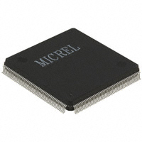
208-Pin PQFP (PQ)
MICREL, INC. 2180 FORTUNE DRIVE SAN JOSE, CA 95131 USA
TEL +1 (408) 944-0800 FAX +1 (408) 474-1000 WEB http:/www.micrel.com
The information furnished by Micrel in this data sheet is believed to be accurate and reliable. However, no responsibility is assumed by Micrel for its use. Micrel reserves the right to change circuitry and specifications at any time without notification to the customer. Micrel Products are not designed or authorized for use as components in life support appliances, devices or systems where malfunction of a product can reasonably be expected to result in personal injury. Life support devices or systems are devices or systems that (a) are intended for surgical implant into the body or (b) support or sustain life, and whose failure to perform can be reasonably expected to result in a significant injury to the user. A Purchaser’s use or sale of Micrel Products for use in life support appliances, devices or systems is a Purchaser’s own risk and Purchaser agrees to fully indemnify Micrel for any damages resulting from such use or sale. © 2004 Micrel, Incorporated.
June 2006
39
M9999-060106
�