SM844256
10 Gigabit Ethernet and SONET, 6 Output, Ultra-Low Jitter LVDS Frequency Synthesizer
General Description
The SM844256 provides a low-noise timing solution for high speed, high accuracy synthesis of clock signals. Common applications include SONET, Gigabit Ethernet, 10 Gigabit Ethernet, and similar networking standards. It includes a power reduction methodology, along with a patented RotaryWaveTM architecture that provides a very stable clock with very low noise. Power supplies of either 3.3V or 2.5V are supported, with superior jitter and phase noise performance. The device synthesizes different low noise LVDS output frequencies such as 125MHz, 156.25MHz, 312.5MHz, and 625MHz for Ethernet applications; 77.76MHz, 155.52MHz, 311.04MHz, and 622.08MHz for SONET applications. The crystal reference frequencies used include 25MHz and 19.44Mhz for Ethernet and SONET applications, respectively. The SM844256 is an excellent replacement for IDT Femtoclocks, with improved accuracy, power consumption, waveform integrity, and jitter. Data sheets and support documentation can be found on Micrel’s web site at: www.micrel.com.
Features
• Generates six LVDS outputs • 2.5V or 3.3V operating range • Typical phase jitter @ 125MHz (1.875MHz to 20MHz): 80 fs (typical) @ 3.3V • 75MHz to 625MHz output frequencies • Industrial temperature range • Green, RoHS, and PFOS compliant • Available in 24-pin TSSOP EPAD • Operating supply modes: Core/Output 3.3V/3.3V, 3.3V/2.5V, 2.5V/2.5V
Applications
• • • • SONET Gigabit Ethernet 10-Gigabit Ethernet Infiniband
________________________________________________________________________________________________________________________
Block Diagram
Micrel Inc. • 2180 Fortune Drive • San Jose, CA 95131 • USA • tel +1 (408) 944-0800 • fax + 1 (408) 474-1000 • http://www.micrel.com
July 2010
M9999-072110-B
�Micrel, Inc.
SM844256
Ordering Information(1, 2)
Part Number SM844256KA
Notes: 1. Devices are Green, RoHS, and PFOS Compliant. 2. Lead finish is 100% matte tin.
Marking 844256
Shipping Tube, Tape & Reel
Junction Temperature Range –40° to +85°C
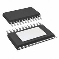
Package 24-Pin TSSOP EPAD
Pin Configuration
24-Pin TSSOP EPAD (Top View)
July 2010
2
M9999-072110-B
�Micrel, Inc.
SM844256
Pin Description
Pin Number 1, 2 3, 4 5, 6 7, 8 9 10 11 12 13 14 15 16, 17 18 19, 20 21, 22 23, 24 Pin Name VDDO /Q2, Q2 /Q1, Q1 /Q0, Q0 PLL_BYPASS VDDA VDD FB_SEL XTAL_IN XTAL_OUT N_SEL0 GND N_SEL1 /Q5, Q5 /Q4, Q4 /Q3, Q3 Pin Type PWR O, (DIF) O, (DIF) O, (DIF) I, (SE) PWR PWR I, (SE) I, (SE) O, (SE) I, (SE) PWR I, (SE) O, (DIF) O, (DIF) O, (DIF) LVCMOS LVDS LVDS LVDS LVCMOS 12pF crystal 12pF crystal LVCMOS LVDS LVDS LVDS LVCMOS Pin Level Pin Function 2.5V or 3.3V Power Supply Differential Clock Output Differential Clock Output Differential Clock Output Pull-Up 45k, Single-Ended Input Select Pin. Logic (0) = PLL Output Logic (1) = Xtal Reference Analog 3.3V or 2.5V Power Supply 3.3V or 2.5V Power Supply Pull-Down 45k, Single-Ended Input Select Pin Crystal Reference Input, no load caps needed. Crystal Reference Output, no load caps needed. Pull-Up 45k, Single-Ended Input Select Pin Ground Pull-Up 45k, Single-Ended Input Select Pin Differential Clock Output Differential Clock Output Differential Clock Output
Input and Output Frequency Table
XTAL (MHz)
24 24 24 24 25 25 25 25 18.75 18.75 18.75 18.75 19.44 19.44 19.44 19.44 19.53125 19.53125 19.53125 19.53125
FB_SEL
0 0 0 0 0 0 0 0 1 1 1 1 1 1 1 1 1 1 1 1
N_SEL1
0 0 1 1 0 0 1 1 0 0 1 1 0 0 1 1 0 0 1 1
N_SEL0
0 1 0 1 0 1 0 1 0 1 0 1 0 1 0 1 0 1 0 1
Outputs (MHz)
600 300 150 120 625 312.50 156.25 125 600 300 150 75 622.08 311.04 155.52 77.76 625 312.5 156.25 78.125
Application
SAS/SATA 10 Gigabit Ethernet 10 Gigabit Ethernet 10 Gigabit Ethernet Gigabit Ethernet/Infiniband/PCI/PCIE/PCI-X SAS/SATA SAS/SATA 10 Gigabit Ethernet/SONET SONET SONET SONET 10 Gigabit Ethernet 10 Gigabit Ethernet 10 Gigabit Ethernet 10 Gigabit Ethernet
July 2010
3
M9999-072110-B
�Micrel, Inc.
SM844256
Absolute Maximum Ratings(1)
Supply Voltage (VDDA, VDD, VDDO)................................+4.6V Input Voltage (VIN)………………………-0.50V to VDD+0.5V LVDS Output Current (IOUT)………………………… ±10mA Lead Temperature (soldering, 20sec.)....................... 260°C Case Temperature ..................................................... 115°C Storage Temperature (Ts) ..........................-65°C to +150°C
Operating Ratings(2)
Supply Voltage (VDDO) .......................... +2.375V to +3.465V Supply Voltage (VDD,VDDA).................... +2.375V to +3.465V Ambient Temperature (TA) .......................... –40°C to +85°C (3) Junction Thermal Resistance TSSOP (θJA).......................................................32°C/W
DC Electrical Characteristics(4)
VDDA = VDD = 3.3V ±5% or 2.5V ±5%, VDDO = 2.5V ±5%, TA = –40°C to +85°C, unless noted.
Symbol VDDO VDDA,VDD IDDA IDD IDDO Parameter 2.5V Operating Voltage 3.3V Operating Voltage Analog Supply Range Core Supply Current I/O Supply Range FOUT = 156.25 MHz FOUT = 625.00 MHz FOUT = 156.25 MHz FOUT = 625.00 MHz FOUT = 156.25 MHz FOUT = 625.00 MHz Condition Min 2.375 2.375 Typ 2.5 3.3 55 56 13 13 195 200 TBD mA TBD mA Max 2.625 3.465 TBD Units V V mA
VDDA = VDD = VDDO = 3.3V ±5%, TA = –40°C to +85°C, unless noted.
Symbol VDDA, VDD, VDDO IDDA IDD IDDO Parameter 3.3V Operating Voltage Condition Min 3.135 Typ 3.3 Max 3.465 Units V
Analog Supply Range Core Supply Current I/O Supply Range
FOUT = 156.25 MHz FOUT = 625.00 MHz FOUT = 156.25 MHz FOUT = 625.00 MHz FOUT = 156.25 MHz FOUT = 625.00 MHz
55 56 13 13 195 200
65 17 234
mA mA mA
Notes: 1. Permanent device damage may occur if absolute maximum ratings are exceeded. This is a stress rating only and functional operation is not implied at conditions other than those detailed in the operational sections of this data sheet. Exposure to absolute maximum rating conditions for extended periods may affect device reliability. 2. The data sheet limits are not guaranteed if the device is operated beyond the operating ratings. 3. Package thermal resistance assumes exposed pad is soldered (or equivalent) to the devices most negative potential on the PCB. 4. The circuit is designed to meet the DC specifications shown in the above table after thermal equilibrium has been established.
July 2010
4
M9999-072110-B
�Micrel, Inc.
SM844256
LVDS DC Electrical Characteristics(5, 6, 7)
VDDA = VDD = 3.3V ±5% or 2.5V ±5%, VDDO = 2.5V or 3.3V ±5%, TA = –40°C to +85°C, unless noted.
Symbol VOD ΔVOD VOS ΔVOS Parameter Differential Output Voltage VOD Magnitude Change Offset Voltage VOS Magnitude Change 1.15 1.25 Condition Figure 1 Min 275 Typ 350 Max 475 40 1.50 50 Units mV mV V mV
LVCMOS DC Electrical Characteristics(6)
VDDA = VDD = 3.3V ±5% or 2.5V ±5%, VDDO = 2.5V or 3.3V ±5%, TA = –40°C to +85°C, unless noted.
Symbol VIH VIL IIH IIH IIL IIL Parameter Input High Voltage Input Low Voltage Input High Current (FB_SEL) Input High Current (PLL_BYPASS), (N_SEL0), (NSEL1) Input Low Current (FB_SEL) Input Low Current (PLL_BYPASS), (N_SEL0), (NSEL1) VDD = VIN = 3.465V VDD = VIN = 3.465V VDD = 3.465V, VIN = 0V VDD = 3.465V, VIN = 0V -5 -150 Condition Min 2 -0.3 Typ Max VDD +0.3 0.8 150 5 Units V V μA μA μA μA
AC Electrical Characteristics(8)
VDDA = VDD = 3.3V ±5% or 2.5V ±5%, VDDO = 2.5V or 3.3V ±5%, TA = –40°C to +85°C, unless noted.
Symbol FOUT Tjit(∅) TSKEW TR/TF ODC TLOCK
Notes: 5. See Figure 4 for load test circuit example. 6. The circuit is designed to meet the DC specifications shown in the above table(s) after thermal equilibrium has been established. 7. Outputs terminated 100Ω between Q and /Q. All unused outputs must be terminated. 8. The circuit is designed to meet the AC specifications shown in the above table(s) after thermal equilibrium has been established. 9. Defined as skew between outputs at the same supply voltage and with equal load conditions. Measured at the output differential crossing points.
Parameter Output Frequency RMS Phase Jitter (Random) Output-to-Output Skew LVDS Output Rise/Fall Time Output Duty Cycle PLL Lock Time
Condition Refer to Frequency Table 125MHz, Integration Range: (1.875MHz – 20MHz) Note 9 20% – 80%
Min 75
Typ 80
Max 625
Units MHz fs
65 100 45 160 50 300 55 20
ps ps % ms
July 2010
5
M9999-072110-B
�Micrel, Inc.
SM844256
Phase Noise Plot: 125MHz @ 3.3V
Figure 1. Duty Cycle Timing
Figure 2. All Outputs Rise/Fall Time
July 2010
6
M9999-072110-B
�Micrel, Inc.
SM844256
Figure 3. RMS Phase Noise/Jitter
Figure 4. LVDS Output Load and Test Circuit
Figure 5. Crystal Input Interface
July 2010
7
M9999-072110-B
�Micrel, Inc.
SM844256
Package Information
24-pin Epad TSSOP
MICREL, INC. 2180 FORTUNE DRIVE SAN JOSE, CA 95131 USA
TEL +1 (408) 944-0800 FAX +1 (408) 474-1000 WEB http://www.micrel.com
The information furnished by Micrel in this data sheet is believed to be accurate and reliable. However, no responsibility is assumed by Micrel for its use. Micrel reserves the right to change circuitry and specifications at any time without notification to the customer. Micrel Products are not designed or authorized for use as components in life support appliances, devices or systems where malfunction of a product can reasonably be expected to result in personal injury. Life support devices or systems are devices or systems that (a) are intended for surgical implant into the body or (b) support or sustain life, and whose failure to perform can be reasonably expected to result in a significant injury to the user. A Purchaser’s use or sale of Micrel Products for use in life support appliances, devices or systems is a Purchaser’s own risk and Purchaser agrees to fully indemnify Micrel for any damages resulting from such use or sale. © 2010 Micrel, Incorporated.
July 2010
8
M9999-072110-B
�