23A256/23K256
256K SPI Bus Low-Power Serial SRAM
Device Selection Table
Part Number 23K256 23A256 VCC Range 2.7-3.6V 1.5-1.95V Page Size 32 Byte 32 Byte Temp. Ranges I, E I Packages P, SN, ST P, SN, ST
Features:
• Max. Clock 20 MHz • Low-Power CMOS Technology: - Read Current: 3 mA at 1 MHz - Standby Current: 4 A Max. at +85°C • 32,768 x 8-bit Organization • 32-Byte Page • HOLD pin • Flexible Operating modes: - Byte read and write - Page mode (32 Byte Page) - Sequential mode • Sequential Read/Write • High Reliability • Temperature Ranges Supported: - Industrial (I): -40C to +85C -40C to +125C - Automotive (E): • Pb-Free and RoHS Compliant, Halogen Free
Description:
The Microchip Technology Inc. 23X256 are 256 Kbit Serial SRAM devices. The memory is accessed via a simple Serial Peripheral Interface (SPI) compatible serial bus. The bus signals required are a clock input (SCK) plus separate data in (SI) and data out (SO) lines. Access to the device is controlled through a Chip Select (CS) input. Communication to the device can be paused via the hold pin (HOLD). While the device is paused, transitions on its inputs will be ignored, with the exception of Chip Select, allowing the host to service higher priority interrupts. The 23X256 is available in standard packages including 8-lead PDIP and SOIC, and advanced packaging including 8-lead TSSOP.
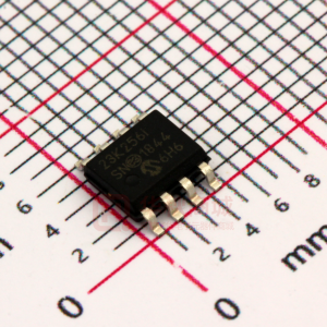
Package Types (not to scale)
Pin Function Table
Name CS SO VSS SI SCK HOLD VCC Function Chip Select Input Serial Data Output Ground Serial Data Input Serial Clock Input Hold Input Supply Voltage PDIP/SOIC/TSSOP (P, SN, ST) CS SO NC VSS 1 2 3 4 8 7 6 5 VCC HOLD SCK SI
2010 Microchip Technology Inc.
DS22100E-page 1
�23X256
1.0 ELECTRICAL CHARACTERISTICS
Absolute Maximum Ratings (†)
VCC .............................................................................................................................................................................4.5V All inputs and outputs w.r.t. VSS ......................................................................................................... -0.3V to VCC +0.3V Storage temperature .................................................................................................................................-65°C to 150°C Ambient temperature under bias ...............................................................................................................-40°C to 125°C ESD protection on all pins ...........................................................................................................................................2kV † NOTICE: Stresses above those listed under “Absolute Maximum Ratings” may cause permanent damage to the device. This is a stress rating only and functional operation of the device at those or any other conditions above those indicated in the operational listings of this specification is not implied. Exposure to maximum rating conditions for an extended period of time may affect device reliability.
TABLE 1-1:
DC CHARACTERISTICS
Industrial (I): TA = -40°C to +85°C Automotive (E): TA = -40°C to +125°C Min. 1.5 2.7 .7 VCC -0.3 — VCC -0.5 — — — — — — Standby current — — 1 5 4 10 7 — 1.2 — Typ(1) — — — — — — — — — — — 0.2 Max. 1.95 3.6 VCC +0.3 0.2xVCC 0.2 — ±0.5 ±0.5 3 6 10 1 Units V V V V V V A A mA mA mA A A A pF V IOL = 1 mA IOH = -400 A CS = VCC, VIN = VSS OR VCC CS = VCC, VOUT = VSS OR VCC FCLK = 1 MHz; SO = O FCLK = 10 MHz; SO = O FCLK = 20 MHz; SO = O CS = VCC = 1.8V, Inputs tied to VCC or VSS CS = VCC = 3.6V, Inputs tied to VCC or VSS CS = VCC = 3.6V, Inputs tied to VCC or VSS @ 125°C VCC = 0V, f = 1 MHz, Ta = 25°C (Note 1) Test Conditions 23A256 (I-Temp) 23K256 (I,E-Temp)
DC CHARACTERISTICS Param. No. D001 D001 D002 D003 D004 D005 D006 D007 D008 Sym. VCC VCC VIH VIL VOL VOH ILI ILO ICC Read Operating current D009 ICCS Characteristic Supply voltage Supply voltage High-level input voltage Low-level input voltage Low-level output voltage High-level output voltage Input leakage current Output leakage current
D010 D011 Note 1: 2:
CINT VDR
Input capacitance RAM data retention voltage (2)
This parameter is periodically sampled and not 100% tested. Typical measurements taken at room temperature (25°C). This is the limit to which VDD can be lowered without losing RAM data. This parameter is periodically sampled and not 100% tested.
DS22100E-page 2
2010 Microchip Technology Inc.
�23X256
TABLE 1-2: AC CHARACTERISTICS
Industrial (I): TA = -40°C to +85°C Automotive (E): TA = -40°C to +125°C Min. — — — — 50 32 32 25 50 50 50 50 50 32 32 25 10 10 10 10 10 10 10 10 — — 50 32 32 25 50 32 32 25 50 32 32 25 — — — — 0 Max. 10 16 16 20 — — — — — — — — — — — — — — — — — — — — 2 2 — — — — — — — — — — — — 50 32 32 25 — Units MHz MHz MHz MHz ns ns ns ns ns ns ns ns ns ns ns ns ns ns ns ns ns ns ns ns us us ns ns ns ns ns ns ns ns ns ns ns ns ns ns ns ns ns Test Conditions VCC 1.5V (I-Temp) VCC 1.8V (I-Temp) VCC 3.0V (E-Temp) VCC 3.0V (I-Temp) VCC 1.5V (I-Temp) VCC 1.8V (I-Temp) VCC 3.0V (E-Temp) VCC 3.0V (I-Temp) VCC 1.5V (I-Temp) VCC 1.8V (I-Temp) VCC 3.0V (E-Temp) VCC 3.0V (I-Temp) VCC 1.5V (I-Temp) VCC 1.8V (I-Temp) VCC 3.0V (E-Temp) VCC 3.0V (I-Temp) VCC 1.5V (I-Temp) VCC 1.8V (I-Temp) VCC 3.0V (E-Temp) VCC 3.0V (I-Temp) VCC 1.5V (I-Temp) VCC 1.8V (I-Temp) VCC 3.0V (E-Temp) VCC 3.0V (I-Temp) Note 1 Note 1 VCC 1.5V (I-Temp) VCC 1.8V (I-Temp) VCC 3.0V (E-Temp) VCC 3.0V (I-Temp) VCC 1.5V (I-Temp) VCC 1.8V (I-Temp) VCC 3.0V (E-Temp) VCC 3.0V (I-Temp) VCC 1.5V (I-Temp) VCC 1.8V (I-Temp) VCC 3.0V (E-Temp) VCC 3.0V (I-Temp) VCC 1.5V (I-Temp) VCC 1.8V (I-Temp) VCC 3.0V (E-Temp) VCC 3.0V (I-Temp) Note 1
AC CHARACTERISTICS Param. Sym. No. 1 FCLK Characteristic Clock frequency
2
TCSS
CS setup time
3
TCSH
CS hold time
4
TCSD
CS disable time
5
Tsu
Data setup time
6
THD
Data hold time
7 8 9
TR TF THI
CLK rise time CLK fall time Clock high time
10
TLO
Clock low time
11
TCLD
Clock delay time
12
TV
Output valid from clock low
13 Note 1:
THO
Output hold time
This parameter is periodically sampled and not 100% tested.
2010 Microchip Technology Inc.
DS22100E-page 3
�23X256
TABLE 1-2: AC CHARACTERISTICS (CONTINUED)
Industrial (I): TA = -40°C to +85°C Automotive (E): TA = -40°C to +125°C Min. — — — — 10 10 10 — Max. 20 20 20 20 — — — 50 Units ns ns ns ns ns ns ns ns Test Conditions VCC 1.5V (I-Temp) VCC 1.8V (I-Temp) VCC 3.0V (E-Temp) VCC 3.0V (I-Temp) — — — — AC CHARACTERISTICS Param. Sym. No. 14 TDIS Characteristic Output disable time
15 16 17 18 Note 1:
THS THH THZ THV
HOLD setup time HOLD hold time HOLD low to output High-Z HOLD high to output valid
This parameter is periodically sampled and not 100% tested.
TABLE 1-3:
AC Waveform:
AC TEST CONDITIONS
0.1 VCC to 0.9 VCC 5 ns -40°C to +125°C — 0.5 VCC 0.5 VCC
Input pulse level Input rise/fall time Operating temperature CL = 100 pF Input Output
Timing Measurement Reference Level:
DS22100E-page 4
2010 Microchip Technology Inc.
�23X256
FIGURE 1-1:
CS 15 SCK 17 SO n+2 n+1 n High-Impedance 17 n 5 n n-1 n-1
HOLD TIMING
16 16
15
Don’t Care SI HOLD n+2 n+1 n
FIGURE 1-2:
SERIAL INPUT TIMING
4
CS 2 SCK 5 SI 6 LSB in 7 8 3 11
MSB in
SO
High-Impedance
FIGURE 1-3:
SERIAL OUTPUT TIMING
CS 9 SCK 12 SO MSB out Don’t Care 13 14 LSB out 10 3
SI
2010 Microchip Technology Inc.
DS22100E-page 5
�23X256
2.0
2.1
FUNCTIONAL DESCRIPTION
Principles of Operation
2.3
Read Sequence
The 23X256 is a 32,768-byte Serial SRAM designed to interface directly with the Serial Peripheral Interface (SPI) port of many of today’s popular microcontroller families, including Microchip’s PIC® microcontrollers. It may also interface with microcontrollers that do not have a built-in SPI port by using discrete I/O lines programmed properly in firmware to match the SPI protocol. The 23X256 contains an 8-bit instruction register. The device is accessed via the SI pin, with data being clocked in on the rising edge of SCK. The CS pin must be low and the HOLD pin must be high for the entire operation. Table 2-1 contains a list of the possible instruction bytes and format for device operation. All instructions, addresses and data are transferred MSB first, LSB last. Data (SI) is sampled on the first rising edge of SCK after CS goes low. If the clock line is shared with other peripheral devices on the SPI bus, the user can assert the HOLD input and place the 23X256 in ‘HOLD’ mode. After releasing the HOLD pin, operation will resume from the point when the HOLD was asserted.
The device is selected by pulling CS low. The 8-bit READ instruction is transmitted to the 23X256 followed by the 16-bit address, with the first MSB of the address being a “don’t care” bit. After the correct READ instruction and address are sent, the data stored in the memory at the selected address is shifted out on the SO pin. If operating in Page mode, after the first byte of data is shifted out, the next memory location on the page can be read out by continuing to provide clock pulses. This allows for 32 consecutive address reads. After the 32nd address read the internal address counter wraps back to the byte 0 address in that page. If operating in Sequential mode, the data stored in the memory at the next address can be read sequentially by continuing to provide clock pulses. The internal Address Pointer is automatically incremented to the next higher address after each byte of data is shifted out. When the highest address is reached (7FFFh), the address counter rolls over to address 0000h, allowing the read cycle to be continued indefinitely. The read operation is terminated by raising the CS pin (Figure 2-1).
2.4
Write Sequence
2.2
Modes of Operation
The 23A256/23K256 has three modes of operation that are selected by setting bits 7 and 6 in the STATUS register. The modes of operation are Byte, Page and Burst. Byte Operation – is selected when bits 7 and 6 in the STATUS register are set to 00. In this mode, the read/ write operations are limited to only one byte. The Command followed by the 16-bit address is clocked into the device and the data to/from the device is transferred on the next 8 clocks (Figure 2-1, Figure 2-2). Page Operation – is selected when bits 7 and 6 in the STATUS register are set to 10. The 23A256/23K256 has 1024 pages of 32 Bytes. In this mode, the read and write operations are limited to within the addressed page (the address is automatically incremented internally). If the data being read or written reaches the page boundary, then the internal address counter will increment to the start of the page (Figure 2-3, Figure 2-4). Sequential Operation – is selected when bits 7 and 6 in the STATUS register are set to 01. Sequential operation allows the entire array to be written to and read from. The internal address counter is automatically incremented and page boundaries are ignored. When the internal address counter reaches the end of the array, the address counter will roll over to 0x0000 (Figure 2-5, Figure 2-6).
Prior to any attempt to write data to the 23X256, the device must be selected by bringing CS low. Once the device is selected, the Write command can be started by issuing a WRITE instruction, followed by the 16-bit address, with the first MSB of the address being a “don’t care” bit, and then the data to be written. A write is terminated by the CS being brought high. If operating in Page mode, after the initial data byte is shifted in, additional bytes can be shifted into the device. The Address Pointer is automatically incremented. This operation can continue for the entire page (32 Bytes) before data will start to be overwritten. If operating in Sequential mode, after the initial data byte is shifted in, additional bytes can be clocked into the device. The internal Address Pointer is automatically incremented. When the Address Pointer reaches the highest address (7FFFh), the address counter rolls over to (0000h). This allows the operation to continue indefinitely, however, previous data will be overwritten.
DS22100E-page 6
2010 Microchip Technology Inc.
�23X256
TABLE 2-1:
READ WRITE RDSR WRSR
INSTRUCTION SET
Instruction Format Description Read data from memory array beginning at selected address Write data to memory array beginning at selected address Read STATUS register Write STATUS register
Instruction Name
0000 0011 0000 0010 0000 0101 0000 0001 BYTE READ SEQUENCE
FIGURE 2-1:
CS 0 SCK
1
2
3
4
5
6
7
8
9 10 11
21 22 23 24 25 26 27 28 29 30 31
Instruction SI 0 0 0 0 0 0 1
16-bit Address 1 15 14 13 12 2 1 0 Data Out 7 6 5 4 3 2 1 0
High-Impedance SO
FIGURE 2-2:
CS 0 SCK 1
BYTE WRITE SEQUENCE
2
3
4
5
6
7
8
9 10 11
21 22 23 24 25 26 27 28 29 30 31 Data Byte 2 1 0 7 6 5 4 3 2 1 0
Instruction SI 0 0 0 0 0 0 1
16-bit Address 0 15 14 13 12
High-Impedance SO
2010 Microchip Technology Inc.
DS22100E-page 7
�23X256
FIGURE 2-3:
CS 0 SCK Instruction SI 0 0 0 0 0 01 16-bit Address 1 15 14 13 12 2 1 0 Page X, Word Y 7 6 5 4 3 2 1 0 Page X, Word Y SO High Impedance 1 2 3 4 5 6 7 8 9 10 11 21 22 23 24 25 26 27 28 29 30 31
PAGE READ SEQUENCE
CS 32 33 34 35 36 37 38 39 SCK SI Page X, Word Y+1 SO 7 6 5 4 3 2 1 0 7 6 Page X, Word 31 5 4 3 2 1 0 7 6 Page X, Word 0 5 4 3 2 1 0
FIGURE 2-4:
CS 0 SCK 1 2
PAGE WRITE SEQUENCE
3
4
5
6
7
8
9 10 11 16-bit Address
21 22 23 24 25 26 27 28 29 30 31 Page X, Word Y 2 1 0 7 6 5 4 3 2 1 0
Instruction SI 0 0 0 0 0 01
0 15 14 13 12
Page X, Word Y
CS 32 33 34 35 36 37 38 39 SCK Page X, Word Y+1 SI 7 6 5 4 3 2 1 0 7 6 Page X, Word 31 5 4 3 2 1 0 7 6 Page X, Word 0 5 4 3 2 1 0
DS22100E-page 8
2010 Microchip Technology Inc.
�23X256
FIGURE 2-5:
CS 0 SCK Instruction SI 0 0 0 0 0 01 16-bit Address 1 15 14 13 12 2 1 0 Page X, Word Y SO 7 6 5 4 3 2 1 0 1 2 3 4 5 6 7 8 9 10 11 21 22 23 24 25 26 27 28 29 30 31
SEQUENTIAL READ SEQUENCE
CS SCK SI
Page X, Word 31 SO 7 6 5 4 3 2 1 0 7
Page X+1, Word 0 6 5 4 3 2 1 0 7 6
Page X+1, Word 1 5 4 3 2 1 0
CS SCK SI Page X+1, Word 31 SO 7 6 5 4 3 2 1 0 7 Page X+n, Word 1 6 5 4 3 2 1 0 7 Page X+n, Word 31 6 5 4 3 2 1 0
2010 Microchip Technology Inc.
DS22100E-page 9
�23X256
FIGURE 2-6:
CS 0 SCK Instruction SI 0 0 0 0 0 01 16-bit Address 0 15 14 13 12 2 1 0 7 6 Data Byte 1 5 4 3 2 1 0 1 2 3 4 5 6 7 8 9 10 11 21 22 23 24 25 26 27 28 29 30 31
SEQUENTIAL WRITE SEQUENCE
CS 32 33 34 35 36 37 38 39 40 41 42 43 44 45 46 47 SCK Data Byte 2 SI 7 6 5 4 3 2 1 0 7 6 Data Byte 3 5 4 3 2 1 0 7 6 Data Byte n 5 4 3 2 1 0
DS22100E-page 10
2010 Microchip Technology Inc.
�23X256
2.5 Read Status Register Instruction (RDSR)
The mode bits indicate the operating mode of the SRAM. The possible modes of operation are: 0 0 = Byte mode (default operation) 1 0 = Page mode 0 1 = Sequential mode 1 1 = Reserved Write and read commands are shown in Figure 2-7 and Figure 2-8. The HOLD bit enables the Hold pin functionality. It must be set to a ‘0’ before HOLD pin is brought low for HOLD function to work properly. Setting HOLD to ‘1’ disables feature. Bits 1 through 5 are reserved and should always be set to ‘0’. See Figure 2-7 for the RDSR timing sequence.
The Read Status Register instruction (RDSR) provides access to the STATUS register. The STATUS register may be read at any time. The STATUS register is formatted as follows:
TABLE 2-2:
7 W/R 6 W/R
STATUS REGISTER
5 – 0 4 – 0 3 – 0 2 – 0 1 – 0 0 W/R HOLD
MODE MODE
W/R = writable/readable.
FIGURE 2-7:
CS
READ STATUS REGISTER TIMING SEQUENCE (RDSR)
0 SCK
1
2
3
4
5
6
7
8
9
10
11
12
13
14
15
Instruction SI 0 0 0 0 0 1 0 1 Data from STATUS Register 7 6 5 4 3 2 1 0
High-Impedance SO
2010 Microchip Technology Inc.
DS22100E-page 11
�23X256
2.6 Write Status Register Instruction (WRSR)
The Write Status Register instruction (WRSR) allows the user to write to the bits in the STATUS register as shown in Table 2-2. This allows for setting of the Device operating mode. Several of the bits in the STATUS register must be cleared to ‘0’. See Figure 2-8 for the WRSR timing sequence.
FIGURE 2-8:
CS
WRITE STATUS REGISTER TIMING SEQUENCE (WRSR)
0 SCK
1
2
3
4
5
6
7
8
9
10
11
12
13
14
15
Instruction SI 0 0 0 0 0 0 0 1 7 6
Data to STATUS Register 5 4 3 2 1 0
High-Impedance SO
2.7
Power-On State
The 23X256 powers on in the following state: • The device is in low-power Standby mode (CS = 1) • A high-to-low-level transition on CS is required to enter active state
DS22100E-page 12
2010 Microchip Technology Inc.
�23X256
3.0 PIN DESCRIPTIONS
3.5 Hold (HOLD)
The descriptions of the pins are listed in Table 3-1. The HOLD pin is used to suspend transmission to the 23X256 while in the middle of a serial sequence without having to retransmit the entire sequence again. It must be held high any time this function is not being used. Once the device is selected and a serial sequence is underway, the HOLD pin may be pulled low to pause further serial communication without resetting the serial sequence. The HOLD pin must be brought low while SCK is low, otherwise the HOLD function will not be invoked until the next SCK high-to-low transition. The 23X256 must remain selected during this sequence. The SI, SCK and SO pins are in a highimpedance state during the time the device is paused and transitions on these pins will be ignored. To resume serial communication, HOLD must be brought high while the SCK pin is low, otherwise serial communication will not resume. Lowering the HOLD line at any time will tri-state the SO line. Hold functionality is disabled by the STATUS register bit.
TABLE 3-1:
Name CS SO VSS SI SCK HOLD VCC
PIN FUNCTION TABLE
Function Chip Select Input Serial Data Output Ground Serial Data Input Serial Clock Input Hold Input Supply Voltage
PDIP/SOIC TSSOP 1 2 4 5 6 7 8
3.1
Chip Select (CS)
A low level on this pin selects the device. A high level deselects the device and forces it into Standby mode. When the device is deselected, SO goes to the highimpedance state, allowing multiple parts to share the same SPI bus. After power-up, a low level on CS is required, prior to any sequence being initiated.
3.2
Serial Output (SO)
The SO pin is used to transfer data out of the 23X256. During a read cycle, data is shifted out on this pin after the falling edge of the serial clock.
3.3
Serial Input (SI)
The SI pin is used to transfer data into the device. It receives instructions, addresses and data. Data is latched on the rising edge of the serial clock.
3.4
Serial Clock (SCK)
The SCK is used to synchronize the communication between a master and the 23X256. Instructions, addresses or data present on the SI pin are latched on the rising edge of the clock input, while data on the SO pin is updated after the falling edge of the clock input.
2010 Microchip Technology Inc.
DS22100E-page 13
�23X256
4.0
4.1
PACKAGING INFORMATION
Package Marking Information
8-Lead PDIP
XXXXXXXX T/XXXNNN YYWW
Example:
23K256 I/P e3 1L7 0528
8-Lead SOIC (3.90 mm)
Example:
XXXXXXXT XXXXYYWW NNN
23K256I SN e3 0528 1L7
8-Lead TSSOP
XXXX TYWW NNN
Example:
K256 I837 1L7
Legend: XX...X T Y YY WW NNN
e3
Note: Note:
Part number or part number code Temperature (I, E) Year code (last digit of calendar year) Year code (last 2 digits of calendar year) Week code (week of January 1 is week ‘01’) Alphanumeric traceability code (2 characters for small packages) Pb-free JEDEC designator for Matte Tin (Sn)
For very small packages with no room for the Pb-free JEDEC designator e3 , the marking will only appear on the outer carton or reel label. In the event the full Microchip part number cannot be marked on one line, it will be carried over to the next line, thus limiting the number of available characters for customer-specific information.
DS22100E-page 14
2010 Microchip Technology Inc.
�23X256
��/HDG 3ODVWLF 'XDO ,Q�/LQH �3� ± ��� PLO %RG\ >3',3@
1RWH� )RU WKH PRVW FXUUHQW SDFNDJH GUDZLQJV� SOHDVH VHH WKH 0LFURFKLS 3DFNDJLQJ 6SHFLILFDWLRQ ORFDWHG DW KWWS���ZZZ�PLFURFKLS�FRP�SDFNDJLQJ
N
NOTE 1 E1
1
2 D
3 E
A
A2
A1
L
c
e b1 b
8QLWV 'LPHQVLRQ /LPLWV 1XPEHU RI 3LQV 3LWFK 7RS WR 6HDWLQJ 3ODQH 0ROGHG 3DFNDJH 7KLFNQHVV %DVH WR 6HDWLQJ 3ODQH 6KRXOGHU WR 6KRXOGHU :LGWK 0ROGHG 3DFNDJH :LGWK 2YHUDOO /HQJWK 7LS WR 6HDWLQJ 3ODQH /HDG 7KLFNQHVV 8SSHU /HDG :LGWK /RZHU /HDG :LGWK 2YHUDOO 5RZ 6SDFLQJ 1 H $ $� $� ( (� ' / F E� E H% ± ���� ���� ���� ���� ���� ���� ���� ���� ���� ± 0,1 ,1&+(6 120 � ���� %6& ± ���� ± ���� ���� ���� ���� ���� ���� ���� ± ���� ���� ± ���� ���� ���� ���� ���� ���� ���� 0$;
eB
���� 1RWHV� �� 3LQ � YLVXDO LQGH[ IHDWXUH PD\ YDU\� EXW PXVW EH ORFDWHG ZLWK WKH KDWFKHG DUHD� �� 6LJQLILFDQW &KDUDFWHULVWLF� �� 'LPHQVLRQV ' DQG (� GR QRW LQFOXGH PROG IODVK RU SURWUXVLRQV� 0ROG IODVK RU SURWUXVLRQV VKDOO QRW H[FHHG ���� SHU VLGH� �� 'LPHQVLRQLQJ DQG WROHUDQFLQJ SHU $60( 62,&@
1RWH� )RU WKH PRVW FXUUHQW SDFNDJH GUDZLQJV� SOHDVH VHH WKH 0LFURFKLS 3DFNDJLQJ 6SHFLILFDWLRQ ORFDWHG DW KWWS���ZZZ�PLFURFKLS�FRP�SDFNDJLQJ
DS22100E-page 18
2010 Microchip Technology Inc.
�23X256
��/HDG 3ODVWLF 7KLQ 6KULQN 6PDOO 2XWOLQH �67� ± ��� PP %RG\ >76623@
1RWH� )RU WKH PRVW FXUUHQW SDFNDJH GUDZLQJV� SOHDVH VHH WKH 0LFURFKLS 3DFNDJLQJ 6SHFLILFDWLRQ ORFDWHG DW KWWS���ZZZ�PLFURFKLS�FRP�SDFNDJLQJ
D N
E E1
NOTE 1
1 b
2 e
c A A2
φ
A1
L1
L
8QLWV 'LPHQVLRQ /LPLWV 1XPEHU RI 3LQV 3LWFK 2YHUDOO +HLJKW 0ROGHG 3DFNDJH 7KLFNQHVV 6WDQGRII 2YHUDOO :LGWK 0ROGHG 3DFNDJH :LGWK 0ROGHG 3DFNDJH /HQJWK )RRW /HQJWK )RRWSULQW )RRW $QJOH /HDG 7KLFNQHVV 1 H $ $� $� ( (� ' / /� I F � ���� ���� ���� ���� ± ���� ���� 0,1
0,//,0(7(56 120 � ���� %6& ± ���� ± ���� %6& ���� ���� ���� ���� 5() ± ± � ���� ���� ���� ���� ���� ���� ���� 0$;
/HDG :LGWK E ���� ± ���� 1RWHV� �� 3LQ � YLVXDO LQGH[ IHDWXUH PD\ YDU\� EXW PXVW EH ORFDWHG ZLWKLQ WKH KDWFKHG DUHD� �� 'LPHQVLRQV ' DQG (� GR QRW LQFOXGH PROG IODVK RU SURWUXVLRQV� 0ROG IODVK RU SURWUXVLRQV VKDOO QRW H[FHHG ���� PP SHU VLGH� �� 'LPHQVLRQLQJ DQG WROHUDQFLQJ SHU $60(