2GB (x72, DR) 244-Pin DDR2 Mini-RDIMM
Features
DDR2 SDRAM Mini-RDIMM
MT18HTF25672PKZ – 2GB
Features
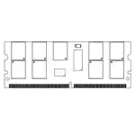
Figure 1:
• 244-pin, mini registered dual in-line memory
module (Mini-RDIMM)
• Fast data transfer rates: PC2-6400, PC2-5300, PC24200, or PC2-3200
• Supports ECC error detection and correction
• VDD = VDDQ = 1.8V
• VDDSPD = 1.7V to 3.6V
• JEDEC-standard 1.8V I/O (SSTL_18-compatible)
• Differential data strobe (DQS, DQS#) option
• 4-bit prefetch architecture
• DLL to align DQ and DQS transitions with CK
• Dual-rank
• Multiple internal device banks for concurrent
operation
• Programmable CAS latency (CL)
• Posted CAS additive latency (AL)
• WRITE latency = READ latency - 1 tCK
• Programmable burst lengths: 4 or 8
• Adjustable data-output drive strength
• 64ms, 8192-cycle refresh
• On-die termination (ODT)
• Serial presence-detect (SPD) with EEPROM
• Gold edge contacts
• Halogen-free
Table 1:
244-Pin Mini-RDIMM (MO-244)
Module Height: 30mm (1.18 in)
Options
Marking
• Operating temperature
– Commercial (0°C TA 70°C)
– Industrial (–40°C TA 85°C)1,2
• Parity
• Package
– 244-pin Mini-RDIMM
(halogen-free)
• Frequency/CAS latency3
– 2.5ns at CL = 5 (DDR2-800)
– 2.5ns at CL = 6 (DDR2-800)
– 3.0ns at CL = 5 (DDR2-667)
I
P
Z
-80E
-800
-667
Notes: 1. Industrial temperature rating applies to
DRAM only.
2. Contact Micron for product availability.
3. CL = CAS (READ) latency; registered mode
will add one clock cycle to CL.
Key Timing Parameters
Data Rate (MT/s)
Speed
Grade
Industry
Nomenclature
CL = 6
CL = 5
CL = 4
CL = 3
(ns)
tRP
(ns)
tRC
(ns)
-80E
-800
-667
-53E
-40E
PC2-6400
PC2-6400
PC2-5300
PC2-4200
PC2-3200
800
800
–
–
–
800
667
667
–
–
533
533
533
533
400
400
400
400
400
400
12.5
15
15
15
15
12.5
15
15
15
15
55
55
55
55
55
PDF: 09005aef83d235f2/Source: 09005aef83d23625
HTF18C256x72PKZ.fm - Rev. B 4/14 EN
1
tRCD
Micron Technology, Inc., reserves the right to change products or specifications without notice.
©2009 Micron Technology, Inc. All rights reserved.
Products and specifications discussed herein are subject to change by Micron without notice.
�2GB (x72, DR) 244-Pin DDR2 Mini-RDIMM
Features
Table 2:
Addressing
2GB
8K
16K A[13:0]
8 BA[2:0]
1Gb (128 Meg x 8)
1K A[9:0]
2 S#[1:0]
Refresh count
Row address
Device bank address
Device configuration
Column address
Module rank address
Table 3:
Part Numbers and Timing Parameters Not Used Modules
Base device: MT47H128M8,11Gb DDR2 SDRAM
Part Number2
Module
Density
Configuration
Module
Bandwidth
Memory Clock/
Data Rate
Latency
(CL - tRCD - tRP)
MT18HTF25672PK(I)Z-80E__
MT18HTF25672PK(I)Z-800__
MT18HTF25672PK(I)Z-667__
2GB
2GB
2GB
256 Meg x72
256 Meg x72
256 Meg x72
6.4 GB/s
6.4 GB/s
5.3 GB/s
2.5ns/800 MT/s
2.5ns/800 MT/s
3.0ns/667MT/s
5-5-5
6-6-6
5-5-5
Notes: 1. The data sheets for the base devices can be found on Micron’s Web site.
2. All part numbers end with a two-place code (not shown), designating component and PCB
revisions. Consult factory for current revision codes. Example: MT18HTF25672PKZ-80EM1.
PDF: 09005aef83d235f2/Source: 09005aef83d23625
HTF18C256x72PKZ.fm - Rev. B 4/14 EN
2
Micron Technology, Inc., reserves the right to change products or specifications without notice.
©2009 Micron Technology, Inc. All rights reserved.
�2GB (x72, DR) 244-Pin DDR2 Mini-RDIMM
Pin Assignments and Descriptions
Pin Assignments and Descriptions
Table 4:
Pin Assignments
244-Pin Mini-RDIMM Front
244-Pin Mini-RDIMM Back
Pin Symbol Pin Symbol Pin Symbol Pin Symbol
Pin Symbol Pin Symbol Pin Symbol Pin Symbol
1
VREF
32
VSS
63
VDDQ
94
DQS5#
123
VSS
154
2
3
4
VSS
DQ0
DQ1
33
34
35
DQ24
DQ25
VSS
64
65
66
A2
VDD
VSS
95
96
97
DQS5
VSS
DQ42
124
125
126
DQ4
DQ5
VSS
155
156
157
5
VSS
36
DQS3#
67
VSS
98
DQ43
127
6
DQS0#
37
DQS3
68
Par_In
99
VSS
128
7
8
9
10
11
12
DQS0
VSS
DQ2
DQ3
VSS
DQ8
38
39
40
41
42
43
VSS
DQ26
DQ27
VSS
CB0
CB1
69
70
71
72
73
74
VDD
A10/AP
BA0
VDD
WE#
VDDQ
100
101
102
103
104
105
DQ48
DQ49
VSS
SA2
NC
VSS
13
DQ9
44
VSS
75
CAS#
106
14
VSS
45
DQS8#
76
VDDQ
15
DQS1#
46
DQS8
77
16
17
18
19
20
21
DQS1
VSS
RESET#
NC
VSS
DQ10
47
48
49
50
51
52
VSS
CB2
CB3
VSS
NC
VDDQ
22
DQ11
53
23
VSS
24
25
26
185
A3
186
187
188
A1
VDD
CK0
189
CK0#
220
VSS
190
VDD
221
DQ52
129
130
131
132
133
134
DM0/
RDQS0
NF/
RDQS0#
VSS
DQ6
DQ7
VSS
DQ12
DQ13
DQ29
VSS
DM3/
RDQS3
158
NF/
RDQS3#
159
VSS
NF/
RDQS5#
217
VSS
218 DQ46
219 DQ47
160
161
162
163
164
165
191
192
193
194
195
196
A0
BA1
VDD
RAS#
VDDQ
S0#
222
223
224
225
226
227
DQS6#
135
VSS
166
VDDQ
107
DQS6
136
ODT0
S1#
108
VSS
137
A13
230
78
79
80
81
82
83
ODT1
VDDQ
NC
VSS
DQ32
DQ33
109
110
111
112
113
114
DQ50
DQ51
VSS
DQ56
DQ57
VSS
138
139
140
141
142
143
DM1/
RDQS1
NF/
RDQS1#
VSS
NF
NF
VSS
DQ14
DQ15
DM8/ 197
RDQS8
167
NF/
198
RDQS8#
168
VSS
199
169
170
171
172
173
174
CB6
CB7
VSS
NC
VDDQ
CKE1
200
201
202
203
204
205
VDD
NC
VSS
DQ36
DQ37
VSS
231
232
233
234
235
236
CKE0
84
VSS
115
DQS7#
144
VSS
175
VDD
206
54
VDD
85
DQS4#
116
DQS7
145
DQ20
176
A15
207
DQ16
DQ17
VSS
55
56
57
BA2
Err_Out
VDDQ
86
87
88
DQS4
VSS
DQ34
117
118
119
VSS
DQ58
DQ59
146
147
148
177
178
179
A14
VDDQ
A12
208
209
210
239
240
241
DQ62
DQ63
VSS
27
DQS2#
58
A11
89
DQ35
120
VSS
149
180
A9
211
VSS
242
SDA
28
29
30
31
DQS2
VSS
DQ18
DQ19
59
60
61
62
A7
VDD
A5
A4
90
91
92
93
VSS
DQ40
DQ41
VSS
121
122
SA0
SA1
150
151
152
153
DQ21
VSS
DM2/
RDQS2
NF/
RDQS2#
VSS
DQ22
DQ23
VSS
DM4/
RDQS4
NF/
RDQS4#
VSS
DQ38
DQ39
181
182
183
184
VDD
A8
A6
VDDQ
212
213
214
215
DQ44
DQ45
VSS
DM5/
RDQS5
243
244
SCL
VDDSPD
PDF: 09005aef83d235f2/Source: 09005aef83d23625
HTF18C256x72PKZ.fm - Rev. B 4/14 EN
3
DQ28
DQ30
DQ31
VSS
CB4
CB5
VSS
216
DQ53
VSS
NC
NC
VSS
DM6/
RDQS6
228
NF/
RDQS6#
229
VSS
DQ54
DQ55
VSS
DQ60
DQ61
VSS
DM7/
RDQS7
237
NF/
RDQS7#
238
VSS
Micron Technology, Inc., reserves the right to change products or specifications without notice.
©2009 Micron Technology, Inc. All rights reserved.
�2GB (x72, DR) 244-Pin DDR2 Mini-RDIMM
Pin Assignments and Descriptions
Table 5:
Pin Descriptions
Symbol
Type
A[15:0]
Input
(SSTL_18)
BA[2:0]
Input
(SSTL_18)
CK0, CK0#
Input
(SSTL_18)
CKE[1:0]
Input
(SSTL_18)
Input
(SSTL_18)
DM[8:0]
RDQS[8:0]
RDQS#[8:0]
ODT[1:0]
Input
(SSTL_18)
Par_In
RAS#, CAS#,
WE#
RESET#
Input
Input
(SSTL_18)
Input
S#[1:0]
SA[2:0]
Input
(SSTL_18)
Input
SCL
Input
CB[7:0]
DQ[63:0]
DQS[8:0],
DQS#[8:0]
I/O
I/O
(SSTL_18)
I/O
(SSTL_18)
SDA
I/O
Err_Out
VDD/VDDQ
VDDSPD
VREF
VSS
NC
Description
Address inputs: Provide the row address for ACTIVE commands, and the column address
and auto precharge bit (A10) for READ/WRITE commands, to select one location out of the
memory array in the respective bank. A10 sampled during a PRECHARGE command
determines whether the PRECHARGE applies to one device bank (A10 LOW, device bank
selected by BA[2:0]) or all device banks (A10 HIGH). The address inputs also provide the opcode during a LOAD MODE command. A[13:0] 2GB. A[15:14] are connected for parity.
Bank address inputs: BA[2:0] define the device bank to which an ACTIVE, READ, WRITE,
or PRECHARGE command is being applied. BA[2:0] define which mode register (MR, EMR1,
EMR2, and EMR3) is loaded during the LOAD MODE command.
Clock: CK and CK# are differential clock inputs. All control, command, and address input
signals are sampled on the crossing of the positive edge of CK and the negative edge of
CK#.
Clock enable: CKE enables (registered HIGH) and disables (registered LOW) internal
circuitry and clocks on the DDR2 SDRAM.
Input data mask: DM is an input mask signal for write data. Input data is masked when
DM is sampled HIGH, along with the input data, during a write access. DM is sampled on
both edges of DQS. Although the DM pins are input-only, DM loading is designed to match
that of the DQ and DQS pins. If RDQS is disabled, RDQS[8:0] become DM[8:0] and
RDQS#[8:0] are no function.
On-die termination: ODT enables (registered HIGH) and disables (registered LOW)
termination resistance internal to the DDR2 SDRAM. When enabled in normal operation,
ODT is only applied to the following pins: DQ, DQS, DQS#, DM, and CB. The ODT input will
be ignored if disabled via the LOAD MODE command.
Parity input: Parity bit for the address, RAS#, CAS#, and WE#.
Command inputs: RAS#, CAS#, and WE# (along with S#) define the command being
entered.
Reset: Asynchronously forces all registered outputs LOW when RESET# is LOW. This signal
can be used during power-up to ensure that CKE is LOW and DQ are High-Z.
Chip select: S# enables (registered LOW) and disables (registered HIGH) the command
decoder.
Serial address inputs: These pins are used to configure the SPD EEPROM address range
on the I2C bus.
Serial clock for SPD EEPROM: SCL is used to synchronize communication to and from the
SPD EEPROM.
Check bits.
Data input/output: Bidirectional data bus.
Data strobe: Output with read data. Edge-aligned with read data. Input with write data.
Center-aligned with write data. DQS# is only used when differential data strobe mode is
enabled via the LOAD MODE command.
Serial data: SDA is a bidirectional pin used to transfer addresses and data into and out of
the SPD EEPROM on the module on the I2C bus.
Parity error output: Parity error found on the command and address bus.
Output
(open drain)
Supply
Power supply: 1.8V ±0.1V. The component VDD and VDDQ are connected to the module
VDD.
Supply
SPD EEPROM power supply: +1.7V to +3.6V.
Supply
Reference voltage: VDD/2.
Supply
Ground.
–
No connect: These pins are not connected on the module.
PDF: 09005aef83d235f2/Source: 09005aef83d23625
HTF18C256x72PKZ.fm - Rev. B 4/14 EN
4
Micron Technology, Inc., reserves the right to change products or specifications without notice.
©2009 Micron Technology, Inc. All rights reserved.
�2GB (x72, DR) 244-Pin DDR2 Mini-RDIMM
Pin Assignments and Descriptions
Table 5:
Pin Descriptions (continued)
Symbol
Type
NF
–
PDF: 09005aef83d235f2/Source: 09005aef83d23625
HTF18C256x72PKZ.fm - Rev. B 4/14 EN
Description
No function: These pins are connected within the module but provide no functionality.
5
Micron Technology, Inc., reserves the right to change products or specifications without notice.
©2009 Micron Technology, Inc. All rights reserved.
�2GB (x72, DR) 244-Pin DDR2 Mini-RDIMM
Functional Block Diagram
Functional Block Diagram
Figure 2:
Functional Block Diagram
RS1#
RS0#
DQS0
DQS0#
DM0/RDQS0
NF/RDQS0#
DQS4
DQS4#
DM4/RDQS4
NF/RDQS4#
DM/
RDQS
DQ0
DQ1
DQ2
DQ3
DQ4
DQ5
DQ6
DQ7
DQ
DQ
DQ
DQ
DQ
DQ
DQ
DQ
NF/ CS# DQS DQS#
RDQS#
U8
DM/
RDQS
DQ
DQ
DQ
DQ
DQ
DQ
DQ
DQ
NF/ CS# DQS DQS#
RDQS#
DM/
RDQS
DQ
DQ
DQ
DQ
DQ
DQ
DQ
DQ
DQ32
DQ33
DQ34
DQ35
DQ36
DQ37
DQ38
DQ39
U22
DQS1
DQS1#
DM1/RDQS1
NF/RDQS1#
NF/ CS# DQS DQS#
RDQS#
U11
DM/
RDQS
DQ
DQ
DQ
DQ
DQ
DQ
DQ
DQ
NF/ CS# DQS DQS#
RDQS#
U20
DQS5
DQS5#
DM5/RDQS5
NF/RDQS5#
DQ8
DQ9
DQ10
DQ11
DQ12
DQ13
DQ14
DQ15
DM/
RDQS
DQ
DQ
DQ
DQ
DQ
DQ
DQ
DQ
NF/ CS# DQS DQS#
RDQS#
U1
DM/
RDQS
DQ
DQ
DQ
DQ
DQ
DQ
DQ
DQ
NF/ CS# DQS DQS#
RDQS#
DM/
RDQS
DQ
DQ
DQ
DQ
DQ
DQ
DQ
DQ
DQ40
DQ41
DQ42
DQ43
DQ44
DQ45
DQ46
DQ47
U18
DQS2
DQS2#
DM2/RDQS2
NF/RDQS2#
NF/ CS# DQS DQS#
RDQS#
U6
DM/
RDQS
DQ
DQ
DQ
DQ
DQ
DQ
DQ
DQ
NF/ CS# DQS DQS#
RDQS#
U14
DQS6
DQS6#
DM6/RDQS6
NF/RDQS6#
DM/
RDQS
DQ16
DQ17
DQ18
DQ19
DQ20
DQ21
DQ22
DQ23
DQ
DQ
DQ
DQ
DQ
DQ
DQ
DQ
NF/ CS# DQS DQS#
RDQS#
U2
DM/
RDQS
DQ
DQ
DQ
DQ
DQ
DQ
DQ
DQ
NF/ CS# DQS DQS#
RDQS#
DM/
RDQS
DQ
DQ
DQ
DQ
DQ
DQ
DQ
DQ
DQ48
DQ49
DQ50
DQ51
DQ52
DQ53
DQ54
DQ55
U17
DQS3
DQS3#
DM3/RDQS3
NF/RDQS3#
NF/ CS# DQS DQS#
RDQS#
U7
DM/
RDQS
DQ
DQ
DQ
DQ
DQ
DQ
DQ
DQ
NF/ CS# DQS DQS#
RDQS#
U13
DQS7
DQS7#
DM7/RDQS7
NF/RDQS7#
DM/
RDQS
DQ24
DQ25
DQ26
DQ27
DQ28
DQ29
DQ30
DQ31
DQ
DQ
DQ
DQ
DQ
DQ
DQ
DQ
NF/ CS# DQS DQS#
RDQS#
U9
DM/
RDQS
DQ
DQ
DQ
DQ
DQ
DQ
DQ
DQ
NF/ CS# DQS DQS#
RDQS#
DM/
RDQS
DQ
DQ
DQ
DQ
DQ
DQ
DQ
DQ
DQ56
DQ57
DQ58
DQ59
DQ60
DQ61
DQ62
DQ63
U21
NF/ CS# DQS DQS#
RDQS#
U12
DM/
RDQS
DQ
DQ
DQ
DQ
DQ
DQ
DQ
DQ
NF/ CS# DQS DQS#
RDQS#
U19
DQS8
DQS8#
DM8/RDQS8
NF/RDQS8#
DM/
RDQS
CB0
CB1
CB2
CB3
CB4
CB5
CB6
CB7
DQ
DQ
DQ
DQ
DQ
DQ
DQ
DQ
NF/ CS# DQS DQS#
RDQS#
U3
DM/
RDQS
DQ
DQ
DQ
DQ
DQ
DQ
DQ
DQ
NF/ CS# DQS DQS#
RDQS#
Rank0 = U1 - U3, U6 - U9, U11, U12
Rank1 = U13, U14, U16 - U22
U16
DDR2 SDRAM x 2
DDR2 SDRAM x 2
DDR2 SDRAM x 2
DDR2 SDRAM x 2
DDR2 SDRAM x 2
DDR2 SDRAM x 2
DDR2 SDRAM x 2
DDR2 SDRAM x 2
DDR2 SDRAM x 2
Register x 2
U10
CK0
CK0#
PLL
RESET#
U4
U5, U15
S0#
S1#
BA[2:0]
A[15:0]
RAS#
CAS#
WE#
CKE0
CKE1
ODT0
ODT1
Par_In
RESET#
CK#
PDF: 09005aef83d235f2/Source: 09005aef83d23625
HTF18C256x72PKZ.fm - Rev. B 4/14 EN
R
e
g
i
s
t
e
r
s
RS0#: Rank0
RS1#: Rank1
RBA[2:0]: DDR2 SDRAM
RA[13:0]: DDR2 SDRAM
RRAS#: DDR2 SDRAM
RCAS#: DDR2 SDRAM
RWE#: DDR2 SDRAM
RCKE0: Rank0
RCKE1: Rank1
RODT0: Rank0
SCL
SPD EEPROM
WP A0
A1
SDA
A2
VSS SA0 SA1 SA2
VDDSPD
RODT1: Rank1
Err_Out
CK
6
Serial PD
VDD
DDR2 SDRAM
VDDQ
DDR2 SDRAM
VREF
DDR2 SDRAM
VSS
DDR2 SDRAM
Micron Technology, Inc., reserves the right to change products or specifications without notice.
©2009 Micron Technology, Inc. All rights reserved.
�2GB (x72, DR) 244-Pin DDR2 Mini-RDIMM
General Description
General Description
The MT18HTF25672PK(I)Z DDR2 SDRAM module is a high-speed, CMOS, dynamic random-access 2GB memory module, organized in x72 configuration. This DDR2 SDRAM
module uses internally configured eight-bank 1Gb DDR2 SDRAM devices.
DDR2 SDRAM modules use double data rate architecture to achieve high-speed operation. The double data rate architecture is essentially a 4n-prefetch architecture with an
interface designed to transfer two data words per clock cycle at the I/O pins. A single
read or write access for the DDR2 SDRAM module effectively consists of a single 4n-bitwide, one-clock-cycle data transfer at the internal DRAM core and four corresponding
n-bit-wide, one-half-clock-cycle data transfers at the I/O pins.
A bidirectional data strobe (DQS, DQS#) is transmitted externally, along with data, for
use in data capture at the receiver. DQS is a strobe transmitted by the DDR2 SDRAM
device during READs and by the memory controller during WRITEs. DQS is edgealigned with data for READs and center-aligned with data for WRITEs.
These DDR2 SDRAM modules operate from a differential clock (CK and CK#); the crossing of CK going HIGH and CK# going LOW will be referred to as the positive edge of CK.
Commands (address and control signals) are registered at every positive edge of CK.
Input data is registered on both edges of DQS, and output data is referenced to both
edges of DQS, as well as to both edges of CK.
Register and PLL EEPROM Operation
DDR2 SDRAM modules operate in registered mode, where the command/address input
signals are latched in the registers on the rising clock edge and sent to the DDR2 SDRAM
devices on the following rising clock edge (data access is delayed by one clock cycle). A
phase-lock loop (PLL) on the module receives and redrives the differential clock signals
(CK, CK#) to the DDR2 SDRAM devices. The register(s) and PLL reduce clock, control,
command, and address signals loading by isolating DRAM from the system controller.
PLL clock timing is defined by JEDEC specifications and ensured by use of the JEDEC
clock reference board. Registered mode will add one clock cycle to CL.
Parity Operations
The registering clock driver can accept a parity bit from the system’s memory controller,
providing even parity for the control, command, and address bus. Parity errors are
flagged on the Err_Out pin. Systems not using parity are expected to function without
issue if Par_In and Err_Out are left as no connects to the system.
Serial Presence-Detect EEPROM Operation
DDR2 SDRAM modules incorporate serial presence-detect. The SPD data is stored in a
256-byte EEPROM. The first 128 bytes are programmed by Micron to identify the module
type and various SDRAM organizations and timing parameters. The remaining 128 bytes
of storage are available for use by the customer. System READ/WRITE operations
between the master (system logic) and the slave EEPROM device occur via a standard
I2C bus using the DIMM’s SCL (clock) and SDA (data) signals, together with SA[2:0],
which provide eight unique DIMM/EEPROM addresses. Write protect (WP) is connected
to VSS, permanently disabling hardware write protection.
PDF: 09005aef83d235f2/Source: 09005aef83d23625
HTF18C256x72PKZ.fm - Rev. B 4/14 EN
7
Micron Technology, Inc., reserves the right to change products or specifications without notice.
©2009 Micron Technology, Inc. All rights reserved.
�2GB (x72, DR) 244-Pin DDR2 Mini-RDIMM
Electrical Specifications
Electrical Specifications
Stresses greater than those listed in Table 6 may cause permanent damage to the DRAM
devices on the module. This is a stress rating only, and functional operation of the device
at these or any other conditions above those indicated in the operational sections of this
specification is not implied. Exposure to absolute maximum rating conditions for
extended periods may adversely affect reliability.
Table 6:
Absolute Maximum Ratings
Symbol
Parameter
Min
Max
Units
VDD
VDDQ
VDDL
VIN, VOUT
II
VDD supply voltage relative to VSS
VDDQ supply voltage relative to VSS
VDDL supply voltage relative to VSS
Voltage on any pin relative to VSS
RAS#, CAS#, WE# S#,
Input leakage current; Any input 0V VIN VDD;
VREF input 0V VIN 0.95V; (All other pins not under CKE, ODT
test = 0V)
CK, CK#
DM
Output leakage current; 0V VOUT VDDQ; DQs and DQ, DQS, DQS#
ODT are disabled
VREF leakage current; VREF = Valid VREF level
DDR2 SDRAM device operating temperature (case)1 Commercial
Industrial2
–1.0
–0.5
–0.5
–0.5
–5
2.3
2.3
2.3
2.3
5
V
V
V
V
µA
–250
–10
–10
250
10
10
µA
–36
0
–40
36
85
95
µA
°C
°C
IOZ
IVREF
TCASE
Notes: 1. For further information, refer to technical note TN-00-08: Thermal Applications, available
on Micron’s Web site at www.micron.com/technotes.
2. Refresh rate must double when TCASE exceeds 85°C.
PDF: 09005aef83d235f2/Source: 09005aef83d23625
HTF18C256x72PKZ.fm - Rev. B 4/14 EN
8
Micron Technology, Inc., reserves the right to change products or specifications without notice.
©2009 Micron Technology, Inc. All rights reserved.
�2GB (x72, DR) 244-Pin DDR2 Mini-RDIMM
DRAM Operating Conditions
DRAM Operating Conditions
Recommended AC operating conditions are given in the DDR2 component data sheets.
Component specifications are available on Micron’s Web site. Module speed grades correlate with component speed grades, as shown in Table 7.
Table 7:
Module and Component Speed Grades
DDR2 components may exceed the listed module speed grades
Module Speed Grade
Component Speed Grade
-80E
-800
-667
-53E
-40E
-25E
-25
-3
-37E
-5E
Design Considerations
Simulations
Micron memory modules are designed to optimize signal integrity through carefully
designed terminations, controlled board impedances, routing topologies, trace length
matching, and decoupling. However, good signal integrity starts at the system level.
Micron encourages designers to simulate the signal characteristics of the system’s memory bus to ensure adequate signal integrity of the entire memory system.
Power
Operating voltages are specified at the DRAM, not at the edge connector of the module.
Designers must account for any system voltage drops at anticipated power levels to
ensure the required supply voltage is maintained.
PDF: 09005aef83d235f2/Source: 09005aef83d23625
HTF18C256x72PKZ.fm - Rev. B 4/14 EN
9
Micron Technology, Inc., reserves the right to change products or specifications without notice.
©2009 Micron Technology, Inc. All rights reserved.
�2GB (x72, DR) 244-Pin DDR2 Mini-RDIMM
IDD Specifications
IDD Specifications
Table 8:
DDR2 IDD Specifications and Conditions – 2GB (Die Revision H)
Values shown for MT47H128M8 DDR2 SDRAM only and are computed from values specified in the 1Gb
(128 Meg x 8) component data sheet
Parameter/Condition
tCK
tCK
tRC
tRC
=
(IDD),
=
(IDD),
Operating one bank active-precharge current:
t
RAS = tRAS MIN (IDD); CKE is HIGH, S# is HIGH between valid commands; Address bus
inputs are switching; Data bus inputs are switching
Operating one bank active-read-precharge current: IOUT = 0mA; BL = 4,
CL = CL (IDD), AL = 0; tCK = tCK (IDD), tRC = tRC (IDD), tRAS = tRAS MIN (IDD),
t
RCD = tRCD (IDD); CKE is HIGH, S# is HIGH between valid commands; Address bus
inputs are switching; Data pattern is same as IDD4W
Precharge power-down current: All device banks idle; tCK = tCK (IDD); CKE is LOW;
Other control and address bus inputs are stable; Data bus inputs are floating
Precharge quiet standby current: All device banks idle; tCK = tCK (IDD); CKE is
HIGH, S# is HIGH; Other control and address bus inputs are stable; Data bus inputs are
floating
Precharge standby current: All device banks idle; tCK = tCK (IDD); CKE is HIGH, S# is
HIGH; Other control and address bus inputs are switching; Data bus inputs are
switching
Active power-down current: All device banks open;
Fast PDN exit
tCK = tCK (I ); CKE is LOW; Other control and address bus inputs MR[12] = 0
DD
are stable; Data bus inputs are floating
Slow PDN exit
MR[12] = 1
Active standby current: All device banks open; tCK = tCK (IDD), tRAS = tRAS MAX
(IDD), tRP = tRP (IDD); CKE is HIGH, S# is HIGH between valid commands; Other control
and address bus inputs are switching; Data bus inputs are switching
Operating burst write current: All device banks open; Continuous burst writes;
BL = 4, CL = CL (IDD), AL = 0; tCK = tCK (IDD), tRAS = tRAS MAX (IDD), tRP = tRP (IDD);
CKE is HIGH, S# is HIGH between valid commands; Address bus inputs are switching;
Data bus inputs are switching
Operating burst read current: All device banks open; Continuous burst reads,
IOUT = 0mA; BL = 4, CL = CL (IDD), AL = 0; tCK = tCK (IDD), tRAS = tRAS MAX (IDD),
tRP = tRP (I ); CKE is HIGH, S# is HIGH between valid commands; Address bus inputs
DD
are switching; Data bus inputs are switching
Burst refresh current: tCK = tCK (IDD); REFRESH command at every tRFC (IDD)
interval; CKE is HIGH, S# is HIGH between valid commands; Other control and address
bus inputs are switching; Data bus inputs are switching
Self refresh current; CK and CK# at 0V; CKE 0.2V; Other control and address bus
inputs are floating; Data bus inputs are floating
Operating bank interleave read current: All device banks interleaving reads,
IOUT = 0mA; BL = 4, CL = CL (IDD), AL = tRCD (IDD) -1 x tCK (IDD); tCK = tCK (IDD),
tRC = tRC (I ), tRRD = tRRD (I ), tRCD = tRCD (I ); CKE is HIGH, S# is HIGH between
DD
DD
DD
valid commands; Address bus inputs are stable during DESELECTs; Data bus inputs are
switching
Symbol
-80E
-800
-667
Units
IDD01
648
603
mA
IDD11
738
693
mA
IDD2P2
126
126
mA
IDD2Q2
432
432
mA
IDD2N2
504
432
mA
IDD3P2
360
270
mA
180
180
mA
IDD3N2
594
540
mA
IDD4W1
1188
1098
mA
IDD4R1
1143
1053
mA
IDD52
1368
1323
mA
IDD62
126
126
mA
IDD71
1953
1728
mA
Notes: 1. Value calculated as one module rank in this operating condition, all other module ranks in
IDD2P (CKE LOW) mode.
2. Value calculated reflects all module ranks in this operating condition.
PDF: 09005aef83d235f2/Source: 09005aef83d23625
HTF18C256x72PKZ.fm - Rev. B 4/14 EN
10
Micron Technology, Inc., reserves the right to change products or specifications without notice.
©2009 Micron Technology, Inc. All rights reserved.
�2GB (x72, DR) 244-Pin DDR2 Mini-RDIMM
IDD Specifications
Table 9:
DDR2 IDD Specifications and Conditions – 2GB (Die Revision M)
Values shown for MT47H128M8 DDR2 SDRAM only and are computed from values specified in the 1Gb
(128 Meg x 8) component data sheet
Parameter/Condition
t
t
t
t
Operating one bank active-precharge current: CK = CK (IDD), RC = RC (IDD),
t
RAS = tRAS MIN (IDD); CKE is HIGH, S# is HIGH between valid commands; Address bus
inputs are switching; Data bus inputs are switching
Operating one bank active-read-precharge current: IOUT = 0mA; BL = 4,
CL = CL (IDD), AL = 0; tCK = tCK (IDD), tRC = tRC (IDD), tRAS = tRAS MIN (IDD),
t
RCD = tRCD (IDD); CKE is HIGH, S# is HIGH between valid commands; Address bus
inputs are switching; Data pattern is same as IDD4W
Precharge power-down current: All device banks idle; tCK = tCK (IDD); CKE is LOW;
Other control and address bus inputs are stable; Data bus inputs are floating
Precharge quiet standby current: All device banks idle; tCK = tCK (IDD); CKE is
HIGH, S# is HIGH; Other control and address bus inputs are stable; Data bus inputs are
floating
Precharge standby current: All device banks idle; tCK = tCK (IDD); CKE is HIGH, S# is
HIGH; Other control and address bus inputs are switching; Data bus inputs are
switching
Active power-down current: All device banks open;
Fast PDN exit
tCK = tCK (I ); CKE is LOW; Other control and address bus inputs MR[12] = 0
DD
are stable; Data bus inputs are floating
Slow PDN exit
MR[12] = 1
Active standby current: All device banks open; tCK = tCK (IDD), tRAS = tRAS MAX
(IDD), tRP = tRP (IDD); CKE is HIGH, S# is HIGH between valid commands; Other control
and address bus inputs are switching; Data bus inputs are switching
Operating burst write current: All device banks open; Continuous burst writes;
BL = 4, CL = CL (IDD), AL = 0; tCK = tCK (IDD), tRAS = tRAS MAX (IDD), tRP = tRP (IDD);
CKE is HIGH, S# is HIGH between valid commands; Address bus inputs are switching;
Data bus inputs are switching
Operating burst read current: All device banks open; Continuous burst reads,
IOUT = 0mA; BL = 4, CL = CL (IDD), AL = 0; tCK = tCK (IDD), tRAS = tRAS MAX (IDD),
t
RP = tRP (IDD); CKE is HIGH, S# is HIGH between valid commands; Address bus inputs
are switching; Data bus inputs are switching
Burst refresh current: tCK = tCK (IDD); REFRESH command at every tRFC (IDD)
interval; CKE is HIGH, S# is HIGH between valid commands; Other control and address
bus inputs are switching; Data bus inputs are switching
Self refresh current; CK and CK# at 0V; CKE 0.2V; Other control and address bus
inputs are floating; Data bus inputs are floating
Operating bank interleave read current: All device banks interleaving reads,
IOUT = 0mA; BL = 4, CL = CL (IDD), AL = tRCD (IDD) -1 x tCK (IDD); tCK = tCK (IDD),
tRC = tRC (I ), tRRD = tRRD (I ), tRCD = tRCD (I ); CKE is HIGH, S# is HIGH between
DD
DD
DD
valid commands; Address bus inputs are stable during DESELECTs; Data bus inputs are
switching
Symbol
-80E
-800
-667
Units
IDD01
675
630
mA
IDD11
765
720
mA
IDD2P2
180
180
mA
IDD2Q2
432
432
mA
IDD2N2
504
432
mA
IDD3P2
540
504
mA
360
360
mA
IDD3N2
594
540
mA
IDD4W1
1215
1125
mA
IDD4R1
1170
1080
mA
IDD52
1485
1440
mA
IDD62
126
126
mA
IDD71
1980
1755
mA
Notes: 1. Value calculated as one module rank in this operating condition, all other module ranks in
IDD2P (CKE LOW) mode.
2. Value calculated reflects all module ranks in this operating condition.
PDF: 09005aef83d235f2/Source: 09005aef83d23625
HTF18C256x72PKZ.fm - Rev. B 4/14 EN
11
Micron Technology, Inc., reserves the right to change products or specifications without notice.
©2009 Micron Technology, Inc. All rights reserved.
�2GB (x72, DR) 244-Pin DDR2 Mini-RDIMM
Register and PLL Specifications
Register and PLL Specifications
Table 10:
Register Specifications
SSTU32866 devices or equivalent
Parameter
Symbol
Pins
Condition
Min
Max
Units
DC high-level
input voltage
VIH(DC)
SSTL_18
VREF(DC) + 125
VDDQ + 250
mV
DC low-level
input voltage
VIL(DC)
SSTL_18
0
VREF(DC) - 125
mV
AC high-level
input voltage
VIH(AC)
SSTL_18
VREF(DC) + 250
VDD
mV
AC low-level
input voltage
VIL(AC)
Control,
command,
address
Control,
command,
address
Control,
command,
address
Control,
command,
address
Parity output
Parity output
All pins
All pins
All pins
SSTL_18
0
VREF(DC) - 250
mV
1.2
–
–5
–
–
–
0.5
+5
100
40
V
V
µA
µA
mA
–
Varies by
manufacturer
µA
–
Varies by
manufacturer
µA
2.5
3.5
pF
–
Varies by
manufacturer
pF
Output high voltage
Output low voltage
Input current
Static standby
Static operating
VOH
VOL
II
IDD
IDD
Dynamic operating
(clock tree)
IDDD
Dynamic operating
(per each input)
IDDD
Input capacitance
(per device, per pin)
Input capacitance
(per device, per pin)
CI
CI
LVCMOS
LVCMOS
VI = VDDQ or VSSQ
RESET# = VSSQ (IO = 0)
RESET# = VSSQ;
VI = VIH(AC) or VIL(DC)
IO = 0
n/a
RESET# = VDD, VI = VIH(DC) or
VIL(AC), IO = 0; CK and CK#
switching 50% duty cycle
n/a
RESET# = VDD, VI = VIH(AC) or
VIL(AC), IO = 0; CK and CK#
switching 50% duty cycle;
One data input switching at
tCK/2, 50% duty cycle
All inputs
VI = VREF ±250mV;
except RESET#
VDDQ = 1.8V
RESET#
VI = VDDQ or VSSQ
Notes: 1. Timing and switching specifications for the register listed above are critical for proper
operation of the DDR2 SDRAM RDIMMs. These are meant to be a subset of the parameters
for the specific device used on the module. Detailed information for this register is available in JEDEC standard JESD82.
PDF: 09005aef83d235f2/Source: 09005aef83d23625
HTF18C256x72PKZ.fm - Rev. B 4/14 EN
12
Micron Technology, Inc., reserves the right to change products or specifications without notice.
©2009 Micron Technology, Inc. All rights reserved.
�2GB (x72, DR) 244-Pin DDR2 Mini-RDIMM
Register and PLL Specifications
Table 11:
PLL Specifications
CU877 device or equivalent JESD82-8.01
Parameter
Symbol
Pins
Condition
Min
Max
Units
DC high-level input
voltage
DC low-level input
voltage
Input voltage (limits)
VIH
RESET#
LVCMOS
0.65 × VDD
–
V
VIL
RESET#
LVCMOS
–
0.35 × VDD
V
VIN
–
–0.3
VDDQ + 0.3
V
DC high-level input
voltage
DC low-level input
voltage
Input differential-pair
cross voltage
Input differential
voltage
Input differential
voltage
Input current
VIH
RESET#, CK,
CK#
CK, CK#
Differential input
0.65 × VDD
–
V
VIL
CK, CK#
Differential input
–
0.35 × VDD
V
VIX
CK, CK#
Differential input
(VDDQ/2) - 0.15
(VDDQ/2) + 0.15
V
VID(DC)
CK, CK#
Differential input
0.3
VDDQ + 0.4
V
VID(AC)
CK, CK#
Differential input
0.6
VDDQ + 0.4
V
II
RESET#
CK, CK#
VI = VDDQ or VSSQ
VI = VDDQ or VSSQ
RESET# = VSSQ; VI = VIH(AC)
or VIL(DC)
CK = CK# = LOW
CK, CK# = 270 MHz, all
outputs open
(not connected to PCB)
VI = VDDQ or VSSQ
–10
–250
100
+10
+250
–
µA
µA
µA
–
–
500
300
µA
mA
2
3
pF
Output disabled
current
Static supply current
Dynamic supply
IODL
IDDLD
IDD
n/a
CIN
Each input
Input capacitance
Table 12:
PLL Clock Driver Timing Requirements and Switching Characteristics
Parameter
Stabilization time
Input clock slew rate
SSC modulation frequency
SSC clock input frequency deviation
PLL loop bandwidth (–3dB from unity gain)
Symbol
Min
Max
Units
tL
–
1.0
30
0.0
2.0
15
4.0
33
–0.5
–
µs
V/ns
kHz
%
MHz
SLRI
–
–
–
Notes: 1. PLL timing and switching specifications are critical for proper operation of the DDR2
DIMM. This is a subset of parameters for the specific PLL used. Detailed PLL information is
available in JEDEC standard JESD82.
PDF: 09005aef83d235f2/Source: 09005aef83d23625
HTF18C256x72PKZ.fm - Rev. B 4/14 EN
13
Micron Technology, Inc., reserves the right to change products or specifications without notice.
©2009 Micron Technology, Inc. All rights reserved.
�2GB (x72, DR) 244-Pin DDR2 Mini-RDIMM
Register and PLL Specifications
Table 13:
PLL Specifications
CU877 device or equivalent JESD82-8.01
Parameter
Symbol
Pins
Condition
Min
Max
Units
DC high-level input
voltage
DC low-level input
voltage
Input voltage (limits)
VIH
RESET#
LVCMOS
0.65 × VDD
–
V
VIL
RESET#
LVCMOS
–
0.35 × VDD
V
VIN
–
–0.3
VDDQ + 0.3
V
DC high-level input
voltage
DC low-level input
voltage
Input differential-pair
cross voltage
Input differential
voltage
Input differential
voltage
Input current
VIH
RESET#, CK,
CK#
CK, CK#
Differential input
0.65 × VDD
–
V
VIL
CK, CK#
Differential input
–
0.35 × VDD
V
VIX
CK, CK#
Differential input
(VDDQ/2) - 0.15
(VDDQ/2) + 0.15
V
VID(DC)
CK, CK#
Differential input
0.3
VDDQ + 0.4
V
VID(AC)
CK, CK#
Differential input
0.6
VDDQ + 0.4
V
II
RESET#
CK, CK#
VI = VDDQ or VSSQ
VI = VDDQ or VSSQ
RESET# = VSSQ; VI = VIH(AC)
or VIL(DC)
CK = CK# = LOW
CK, CK# = 270 MHz, all
outputs open
(not connected to PCB)
VI = VDDQ or VSSQ
–10
–250
100
+10
+250
–
µA
µA
µA
–
–
500
300
µA
mA
2
3
pF
Output disabled
current
Static supply current
Dynamic supply
IODL
IDDLD
IDD
n/a
CIN
Each input
Input capacitance
Table 14:
PLL Clock Driver Timing Requirements and Switching Characteristics
Parameter
Stabilization time
Input clock slew rate
SSC modulation frequency
SSC clock input frequency deviation
PLL loop bandwidth (–3dB from unity gain)
Symbol
Min
Max
Units
tL
–
1.0
30
0.0
2.0
15
4.0
33
–0.5
–
µs
V/ns
kHz
%
MHz
SLRI
–
–
–
Notes: 1. PLL timing and switching specifications are critical for proper operation of the DDR2
DIMM. This is a subset of parameters for the specific PLL used. Detailed PLL information is
available in JEDEC standard JESD82.
PDF: 09005aef83d235f2/Source: 09005aef83d23625
HTF18C256x72PKZ.fm - Rev. B 4/14 EN
14
Micron Technology, Inc., reserves the right to change products or specifications without notice.
©2009 Micron Technology, Inc. All rights reserved.
�2GB (x72, DR) 244-Pin DDR2 Mini-RDIMM
Serial Presence-Detect
Serial Presence-Detect
Table 15:
Serial Presence-Detect EEPROM DC Operating Conditions
Parameter/Condition
Supply voltage
Input high voltage: Logic 1; All inputs
Input low voltage: Logic 0; All inputs
Output low voltage: IOUT = 3mA
Input leakage current: VIN = GND to VDD
Output leakage current: VOUT = GND to VDD
Standby current
Power supply current, READ: SCL clock frequency = 100 kHz
Power supply current, WRITE: SCL clock frequency = 100 kHz
Table 16:
Symbol
Min
Max
Units
VDDSPD
VIH
VIL
VOL
ILI
ILO
ISB
ICCR
ICCW
1.7
VDDSPD × 0.7
–0.6
–
0.1
0.05
1.6
0.4
2.0
3.6
VDDSPD + 0.5
VDDSPD × 0.3
0.4
3.0
3.0
4.0
1.0
3.0
V
V
V
V
µA
µA
µA
mA
mA
Serial Presence-Detect EEPROM AC Operating Conditions
Parameter/Condition
SCL LOW to SDA data-out valid
Time the bus must be free before a new transition can start
Data-out hold time
SDA fall time
SDA rise time
Data-in hold time
Start condition hold time
Clock HIGH period
Noise suppression time constant at SCL, SDA inputs
Clock LOW period
SCL clock frequency
Data-in setup time
Start condition setup time
Stop condition setup time
WRITE cycle time
Symbol
Min
Max
Units
Notes
tAA
0.2
1.3
200
–
–
0
0.6
0.6
–
1.3
–
100
0.6
0.6
–
0.9
–
–
300
300
–
–
–
50
–
400
–
–
–
10
µs
µs
ns
ns
ns
µs
µs
µs
ns
µs
kHz
ns
µs
µs
ms
1
tBUF
tDH
tF
tR
tHD:DAT
tH:STA
tHIGH
tI
tLOW
fSCL
tSU:DAT
t
SU:STA
tSU:STO
tWRC
2
2
3
4
Notes: 1. To avoid spurious start and stop conditions, a minimum delay is placed between SCL = 1
and the falling or rising edge of SDA.
2. This parameter is sampled.
3. For a restart condition or following a WRITE cycle.
4. The SPD EEPROM WRITE cycle time (tWRC) is the time from a valid stop condition of a
write sequence to the end of the EEPROM internal ERASE/PROGRAM cycle. During the
WRITE cycle, the EEPROM bus interface circuit is disabled, SDA remains HIGH due to pullup resistance, and the EEPROM does not respond to its slave address.
Serial Presence-Detect Data
For the latest serial presence-detect data, refer to Micron's SPD page:
www.micron.com/SPD.
PDF: 09005aef83d235f2/Source: 09005aef83d23625
HTF18C256x72PKZ.fm - Rev. B 4/14 EN
15
Micron Technology, Inc., reserves the right to change products or specifications without notice.
©2009 Micron Technology, Inc. All rights reserved.
�2GB (x72, DR) 244-Pin DDR2 Mini-RDIMM
Module Dimensions
Module Dimensions
Figure 3:
244-Pin DDR2 Mini-RDIMM
Front view
3.8 (0.15)
MAX
82.127 (3.233)
81.873 (3.223)
U4
2.0 (0.079) R
2X
U1
U2
U6
U3
U7
U5
1.0 (0.039) R
2X
U8
U9
U11
U12
U10
1.8 (0.071) D
2X
30.152 (1.187)
29.848 (1.175)
20.0 (0.787)
TYP
10.0 (0.394)
TYP
6.0 (0.236)
TYP
1.0 (0.039)
TYP
2.0 (0.079)
TYP
PIN 1
0.5 (0.02) R
0.6 (0.024) 0.45 (0.018)
TYP
TYP
PIN 122
1.1 (0.043)
0.9 (0.035)
42.9 (1.69)
TYP
78.0 (3.071)
TYP
Back view
45° 4X
U13
U14
U16
U17
U18
U21
U22
U15
U19
U20
3.3 (0.13)
TYP
3.6 (0.142) TYP
Pin 123
Pin 244
33.6 (1.323)
TYP
38.4 (1.521)
TYP
3.2 (0.126)
TYP
Notes: 1. All dimensions are in millimeters (inches), MAX/MIN or typical (TYP) where noted.
2. The dimensional diagram is for reference only. Refer to the JEDEC MO document for complete design dimensions.
8000 S. Federal Way, P.O. Box 6, Boise, ID 83707-0006, Tel: 208-368-3900
www.micron.com/productsupport Customer Comment Line: 800-932-4992
Micron and the Micron logo are trademarks of Micron Technology, Inc.
All other trademarks are the property of their respective owners.
This data sheet contains minimum and maximum limits specified over the power supply and temperature range set forth herein. Although
considered final, these specifications are subject to change, as further product development and data characterization sometimes occur.
PDF: 09005aef83d235f2/Source: 09005aef83d23625
HTF18C256x72PKZ.fm - Rev. B 4/14 EN
16
Micron Technology, Inc., reserves the right to change products or specifications without notice.
©2009 Micron Technology, Inc. All rights reserved.
�