ADVANCE‡
0.16µm Process
512K x 18
2.5V VDD, HSTL, QDRb4 SRAM
9Mb QDR™ SRAM
4-WORD BURST
MT54V512H18E
Features
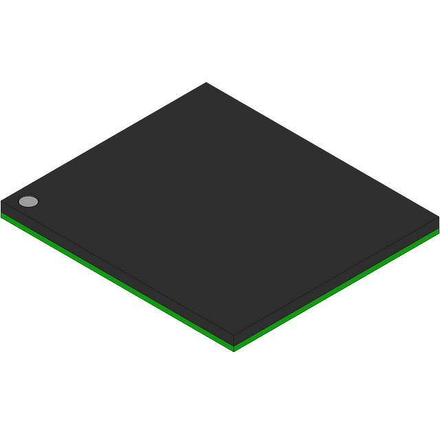
Figure 1:
165-Ball FBGA
• 9Mb Density (512K x 18)
• Separate independent read and write data ports
with concurrent transactions
• 100 percent bus utilization DDR READ and WRITE
operation
• High-frequency operation with future migration to
higher clock frequencies
• Fast clock to valid data times
• Full data coherency, providing most current data
• Four-tick burst counter for reduced address
frequency
• Double data rate operation on read and write ports
• Two input clocks (K and K#) for precise DDR timing
at clock rising edges only
• Two output clocks (C and C#) for precise flight time
and clock skew matching—clock and data delivered
together to receiving device
• Single address bus
• Simple control logic for easy depth expansion
• Internally self-timed, registered writes
• +2.5V core and HSTL I/O
• Clock-stop capability
• 13mm x 15mm, 1mm pitch, 11 x 15 grid FBGA
package
• User-programmable impedance outputs
• JTAG boundary scan
OPTIONS
• Clock Cycle Timing
6ns (167 MHz)
7.5ns (133 MHz)
10nx (100 MHz)
• Configurations
512K x 18
• Package
165-ball, 13mm x 15mm FBGA
Table 1:
PART NUMBER
MT54V512H18EF-xx
512K x 18, QDRb4 FBGA
The Micron® QDR® (Quad Data Rate™) Synchronous Pipelined Burst SRAM employs high-speed, lowpower CMOS designs using an advanced 6T CMOS
process.
The QDR architecture consists of two separate DDR
(double data rate) ports to access the memory array.
The read port has dedicated data outputs to support
READ operations. The write port has dedicated data
inputs to support WRITE operations. This architecture
eliminates the need for high-speed bus turnaround.
Access to each port is accomplished using a common
address bus. Addresses for reads and writes are latched
on alternate rising edges of the K input clock. Each
address location is associated with four 18-bit words
that burst sequentially into or out of the device. Since
data can be transferred into and out of the device on
every rising edge of both clocks (K, K#, C and C#)
memory bandwidth is maximized while simplifying
system design by eliminating bus turnarounds.
MARKING1
-6
-7.5
-10
MT54V512H18E
F
1. A Part Marking Guide for FBGA devices can be found on Micron’s
Web site¾http://www.micron.com/numberguide
‡PRODUCTS
DESCRIPTION
General Description
NOTE:
512K x 18, 2.5V VDD , HSTL, QDRb4 SRAM
MT54V512H18E_16_A.fm - Rev. 10/02
Valid Part Numbers
1
Micron Technology, Inc., reserves the right to change products or specifications without notice.
©2002, Micron Technology Inc.
AND SPECIFICATIONS DISCUSSED HEREIN ARE FOR EVALUATION AND REFERENCE PURPOSES ONLY AND ARE SUBJECT TO CHANGE BY
MICRON WITHOUT NOTICE. PRODUCTS ARE ONLY WARRANTED BY MICRON TO MEET MICRON’S PRODUCTION DATA SHEET SPECIFICATIONS.
�0.16µm Process
ADVANCE
512K x 18
2.5V VDD, HSTL, QDRb4 SRAM
Depth expansion is accomplished with port selects
for each port (read R#, write W#) which are received at
K rising edge. Port selects permit independent port
operation. All synchronous inputs pass through registers controlled by the K or K# input clock rising edges.
Active LOW byte writes (BW0#, BW1#) permit byte
write selection. Write data and byte writes are registered on the rising edges of both K and K#. The
addressing within each burst of four is fixed and
sequential. All synchronous data outputs pass through
output registers controlled by the rising edges of the
output clocks (C and C# if provided, otherwise K and
K#).
Four balls are used to implement JTAG test capabilities: test mode select (TMS), test data-in (TDI), test
clock (TCK), and test data-out (TDO). JTAG circuitry is
used to serially shift data to and from the SRAM. JTAG
inputs use JEDEC-standard 2.5V I/O levels to shift data
during this testing mode of operation.
The SRAM operates from a +2.5V power supply, and
all inputs and outputs are HSTL-compatible. The
device is ideally suited for applications that benefit
from a high-speed fully-utilized DDR data bus.
Please refer to Micron’s Web site (www.micron.com/
sramds) for the latest data sheet.
burst in progress is ignored. The resulting benefit is
that the address rate is kept down to the clock frequency even when both buses are 100 percent utilized.
READ cycles are pipelined. The request is initiated
by asserting R# LOW at K rising edge. Data is delivered
after the next rising edge of K using C and C# as the
output timing references, or using K and K#, if C and
C# are tied HIGH. If C and C# are tied HIGH, they may
not be toggled during device operation. Output tristating is automatically controlled such that the bus is
released if no data is being delivered. This permits
banked SRAM systems with no complex OE timing
generation. Back-to-back READ cycles are initiated
every second K rising edge. Any command in between
is ignored, since the burst sequence may not be interrupted and requires two full clock cycles.
WRITE cycles are initiated by W# LOW at K rising
edge. Data is expected at both rising edges of K andK#
beginning one clock period later. Write registers are
incorporated to facilitate pipelined self-timed WRITE
cycles and provide fully coherent data for all combinations of READs and WRITEs. A READ can immediately
follow a WRITE even if they are to the same address.
Although the WRITE data has not been written to the
memory array, the SRAM will deliver the data from the
write register instead of using the older data from the
memory array. The latest data is always utilized for all
bus transactions. WRITE cycles are initiated every second K rising edge. Any command in between is
ignored, since the burst sequence may not be interrupted.
READ/WRITE Operations
All bus transactions operate on an uninterruptable
burst of four data, requiring two full clock cycles of bus
utilization. Any request that attempts to interrupt a
Figure 2:
Functional Block Diagram: 512K x 18
n
ADDRESS
R#
W#
n
ADDRESS
REGISTRY
& LOGIC
K
W#
BW0#
BW1#
MUX
36
18
D (Data In)
R#
DATA
REGISTRY
& LOGIC
36
K
WR
R E
I G
T
E
WD
R R
I I
T V
E E
R
2 n x 72
MEMORY
ARRAY
36
S
E A
NM
S P
E S
36
O
U
T
P
U
T
S O B
E U U
L T F 18
Q
E P F
C U E (Data Out)
T
R
T
C
MUX
K
K#
OR
U E 72
T G
P
U
T
C,C#
NOTE:
1. The functional block diagram illustrates simplified device operation. See truth tables, ball descriptions, and timing
diagrams for detailed information.
2. n = 17
512K x 18, 2.5V VDD , HSTL, QDRb4 SRAM
MT54V512H18E_16_A.fm - Rev 10/02
2
Micron Technology, Inc., reserves the right to change products or specifications without notice.
©2002, Micron Technology Inc.
�0.16µm Process
ADVANCE
512K x 18
2.5V VDD, HSTL, QDRb4 SRAM
BYTE WRITE Operations
cycles to update the impedance. The user can operate
the part with fewer than 1,024 clock cycles, but optimal
output impedance is not guaranteed.
BYTE WRITE operations are supported. The active
LOW byte write controls, BW0# and BW1#, are registered coincident with their corresponding data. This
feature can eliminate the need for some READ/MODIFY/WRITE cycles, collapsing it to a single BYTE
WRITE operation in some instances.
Clock Considerations
The device does not utilize internal phase-locked
loops and can therefore be placed into a stopped-clock
state to minimize power without lengthy restart times.
It is strongly recommended that the clocks operate for
a number of cycles prior to initiating commands to the
SRAM. This delay permits transmission line charging
effects to be overcome and allows the clock timing to
be nearer to its steady-state value.
Programmable Impedance Output
Buffer
The QDR SRAM is equipped with programmable
impedance output buffers. This allows a user to match
the driver impedance to the system. To adjust the
impedance, an external precision resistor (RQ) is connected between the ZQ ball and VSS. The value of the
resistor must be five times the desired impedance. For
example, a 350W resistor is required for an output
impedance of 70W . To ensure that output impedance
is one fifth the value of RQ (within 15 percent), the
range of RQ is 175W to 350W . Alternately, the ZQ ball
can be connected directly to VDDQ, which will place
the device in a minimum impedance mode.
Output impedance updates may be required
because variations may occur in supply voltage and
temperature over time. The device samples the value
of RQ. Impedance updates are transparent to the system; they do not affect device operation, and all data
sheet timing and current specifications are met during
an update.
The device will power up with an output impedance
set at 50W . To guarantee optimum output driver
impedance after power-up, the SRAM needs 1,024
Single Clock Mode
The SRAM can be used with the single K, K# clock
pair by tying C and C# HIGH. In this mode, the SRAM
will use K and K# in place of C and C#. This mode provides the most rapid data output but does not compensate for system clock skew and flight times.
Depth Expansion
Port select inputs are provided for the read and
write ports. This allows for easy depth expansion. Both
port selects are sampled on the rising edge of K only.
Each port can be independently selected and deselected and do not affect the operation of the opposite
port. All pending transactions are completed prior to a
port deselecting.
Figure 3:
Application Example
SRAM #1
Vt
D
SA
R
B
W
R W n
# # #
ZQ
Q
C C# K K#
DATA IN
DATA OUT
Addresses
Read#
BUS
Write#
MASTER
BWn#
(CPU
or
ASIC)
Return CLK
Source CLK
Return CLK#
Source CLK#
SRAM #4
R = 250Ω
B
W
R W n
# # #
D
SA
R
R = 250Ω
ZQ
Q
C C# K K#
Vt
Vt
Vt
Vt
R = 50Ω Vt = VREF
512K x 18, 2.5V VDD , HSTL, QDRb4 SRAM
MT54V512H18E_16_A.fm - Rev 10/02
3
Micron Technology, Inc., reserves the right to change products or specifications without notice.
©2002, Micron Technology Inc.
�0.16µm Process
ADVANCE
512K x 18
2.5V VDD, HSTL, QDRb4 SRAM
Table 2:
1
Ball Assignment (Top View)
165-Ball FBGA
2
A
DNU
VSS/SA
B
NC
Q9
C
NC
D
3
1
4
2
5
6
7
8
9
10
3
11
4
W#
BW1#
K#
NC
R#
NC/SA
VSS/SA
DNU
D9
SA
NC
K
BW0#
SA
NC
NC
Q8
NC
D10
VSS
SA
NC
SA
VSS
NC
Q7
D8
NC
D11
Q10
VSS
VSS
VSS
VSS
VSS
NC
NC
D7
E
NC
NC
Q11
VDDQ
VSS
VSS
VSS
VDDQ
NC
D6
Q6
F
NC
Q12
D12
VDDQ
VDD
VSS
VDD
VDDQ
NC
NC
Q5
G
NC
D13
Q13
VDDQ
VDD
VSS
VDD
VDDQ
NC
NC
D5
H
NC
VREF
VDDQ
VDDQ
VDD
VSS
VDD
VDDQ
VDDQ
VREF
ZQ
J
NC
NC
D14
VDDQ
VDD
VSS
VDD
VDDQ
NC
Q4
D4
K
NC
NC
Q14
VDDQ
VDD
VSS
VDD
VDDQ
NC
D3
Q3
L
NC
Q15
D15
VDDQ
VSS
VSS
VSS
VDDQ
NC
NC
Q2
M
NC
NC
D16
VSS
VSS
VSS
VSS
VSS
NC
Q1
D2
N
NC
D17
Q16
VSS
SA
SA
SA
VSS
NC
NC
D1
P
NC
NC
Q17
SA
SA
C
SA
SA
NC
D0
Q0
R
TDO
TCK
SA
SA
SA
C#
SA
SA
SA
TMS
TDI
NC/SA
NOTE:
1.
2.
3.
4.
Expansion address: 2A for 144Mb
Expansion address: 3A for 36Mb
Expansion address: 9A for 18Mb
Expansion address: 10A for 72Mb
512K x 18, 2.5V VDD , HSTL, QDRb4 SRAM
MT54V512H18E_16_A.fm - Rev 10/02
4
Micron Technology, Inc., reserves the right to change products or specifications without notice.
©2002, Micron Technology Inc.
�0.16µm Process
ADVANCE
512K x 18
2.5V VDD, HSTL, QDRb4 SRAM
Table 3:
Ball Descriptions
SYMBOL
TYPE
DESCRIPTION
SA
Input
R#
Input
W#
Input
BW0#
BW1#
Input
K
K#
Input
C
C#
Input
TMS
TDI
TCK
Input
VREF
Input
ZQ
Input
D_
Input
DNU
TDO
Q_
Output
Output
Output
VDD
Supply
VDDQ
Supply
VSS
Supply
Synchronous Address Inputs: These inputs are registered and must meet the setup and hold
times around the rising edge of K. See Ball Assignment figures for address expansion inputs.
All transactions operate on a burst of four 18-bit data (two clock periods of bus activity).
These inputs are ignored when both ports are deselected.
Synchronous Read: When LOW, this input causes the address inputs to be registered and a
READ cycle to be initiated. This input must meet setup and hold times around the rising edge
of K and is ignored on the subsequent rising edge of K.
Synchronous Write: When LOW, this input causes the address inputs to be registered and a
WRITE cycle to be initiated. This input must meet setup and hold times around the rising edge
of K and is ignored on the subsequent rising edge of K. This input is also ignored if a READ
cycle is being initiated.
Synchronous Byte Writes: When LOW, these inputs cause their respective bytes to be
registered and written if W# had initiated a WRITE cycle. These signals must meet setup and
hold times around the rising edges of K and K# for each of the four rising edges comprising
the WRITE cycle. BW0# controls D0:D8, and BW1# controls D9:D17. See Ball Assignment
figures for signal to data relationships.
Input Clock: This input clock pair registers address and control inputs on the rising edge of K,
and registers data on the rising edge of K and the rising edge of K#. K# is ideally 180 degrees
out of phase with K. All synchronous inputs must meet setup and hold times around the clock
rising edges.
Output Clock: This clock pair provides a user-controlled means of tuning device output data.
The rising edge of C is used as the output timing reference for second and fourth output data.
The rising edge of C# is used as the output reference for first and third output data. Ideally,
C# is 180 degrees out of phase with C. C and C# may be tied HIGH to force the use of K and K#
as the output reference clocks instead of having to provide C and C# clocks. If tied HIGH, these
inputs may not be allowed to toggle during device operation.
IEEE 1149.1 Test Inputs: 2.5V I/O levels. These balls may be left as No Connects if the JTAG
function is not used in the circuit.
IEEE 1149.1 Clock Input: 2.5V I/O levels. This ball must be tied to VSS if the JTAG function is not
used in the circuit.
HSTL Input Reference Voltage: Nominally VDDQ/2, but may be adjusted to improve system
noise margin. Provides a reference voltage for the HSTL input buffer trip point.
Output Impedance Matching Input: This input is used to tune the device outputs to the
system data bus impedance. DQ output impedance is set to 0.2 x RQ, where RQ is a resistor
from this ball to ground. Alternately, this ball can be connected directly to VDDQ, which
enables the minimum impedance mode. This ball cannot be connected directly to GND or left
unconnected.
Synchronous Data Inputs: Input data must meet setup and hold times around the rising edges
of K and K# during WRITE operations. See Ball Assignment figures for ball site location of
individual signals.
Do Not Use: These balls should not be used.
IEEE 1149.1 Test Output: JEDEC-standard 2.5V I/O level.
Synchronous Data Outputs: Output data is synchronized to the respective C and C# or to K
and K# rising edges if C and C# are tied HIGH. This bus operates in response to R# commands.
See Ball Assignment figures for ball site location of individual signals.
Power Supply: 2.5V nominal. See DC Electrical Characteristics and Operating Conditions for
range.
Power Supply: Isolated Output Buffer Supply. Nominally 1.5V. See DC Electrical Characteristics
and Operating Conditions for range.
Power Supply: GND.
Input
512K x 18, 2.5V VDD , HSTL, QDRb4 SRAM
MT54V512H18E_16_A.fm - Rev 10/02
5
Micron Technology, Inc., reserves the right to change products or specifications without notice.
©2002, Micron Technology Inc.
�0.16µm Process
ADVANCE
512K x 18
2.5V VDD, HSTL, QDRb4 SRAM
Table 3:
Ball Descriptions (Continued)
SYMBOL
TYPE
NC
–
NC/SA
512K x 18, 2.5V VDD , HSTL, QDRb4 SRAM
MT54V512H18E_16_A.fm - Rev 10/02
DESCRIPTION
No Connect: These signals are not internally connected and may be connected to ground to
improve package heat dissipation.
These balls are reserved for higher-order address bits, respectively.
6
Micron Technology, Inc., reserves the right to change products or specifications without notice.
©2002, Micron Technology Inc.
�0.16µm Process
ADVANCE
512K x 18
2.5V VDD, HSTL, QDRb4 SRAM
Figure 4:
Bus Cycle State Diagram
RD
LOAD NEW
READ ADDRESS;
R_Count=0;
R_Init=1
RD & R_Count=4
always
READ DOUBLE;
R_Count=R_Count+2
always
R_Count=2
INCREMENT READ
ADDRESS BY TWO1
R_Init=0
/RD & R_Count=4
WT & R_Init=0
READ PORT NOP
R_Init=0
/RD
Supply
voltage
provided
POWER-UP
Supply
voltage
provided
LOAD NEW
WRITE ADDRESS;
W_Count=0
WT & W_Count=4
WRITE DOUBLE;
W_Count=W_Count+2
always
always
INCREMENT WRITE
ADDRESS BY TWO1
WRITE PORT NOP
/WT
W_Count=2
/WT & W_Count=4
NOTE:
1. The address is concatenated with 2 additional internal LSBs to facilitate burst operation. The address order is always
fixed as: xxx...xxx+0, xxx...xxx+1, xxx...xxx+2, xxx...xxx+3. Bus cycle is terminated at the end of this sequence (burst
count = 4).
2. State transitions: RD = (R# = LOW); WT = (W# = LOW).
3. Read and write state machines can be active simultaneously. Read and write cannot be simultaneously initiated.
Read takes precedence.
4. State machine control timing sequence is controlled by K
512K x 18, 2.5V VDD , HSTL, QDRb4 SRAM
MT54V512H18E_16_A.fm - Rev 10/02
7
Micron Technology, Inc., reserves the right to change products or specifications without notice.
©2002, Micron Technology Inc.
�0.16µm Process
ADVANCE
512K x 18
2.5V VDD, HSTL, QDRb4 SRAM
Table 4:
Truth Table
Notes 1-8
OPERATION
WRITE Cycle:
Load address, input write data on
two consecutive K and K# rising
edges
READ Cycle:
Load address, output data on two
consecutive C and C# rising edges
NOP: No operation
STANDBY: Clock stopped
Table 5:
K
R#
W#
D or Q
D or Q
D or Q
D or Q
L®H
H7
L8
DA(A + 0)
at
K(t + 1)
DA(A + 1)
at
K#(t + 1)
DA(A + 2)
at
K(t + 2)
DA(A + 3)
at
K#(t + 2)
L®H
L8
X
L®H
H
H
Stopped
X
X
QA(A+0)
at
C(t + 1)
D=X
Q = High-Z
Previous
State
QA(A+1)
at
C#(t + 1)
D=X
Q = High-Z
Previous
State
QA(A+2)
at
C(t + 2)
D=X
Q = High-Z
Previous
State
QA(A+3)
at
C#(t + 2)
D=X
Q = High-Z
Previous
State
K#
BW0#
BW1#
0
0
0
0
1
1
1
1
0
0
1
1
0
0
1
1
BYTE WRITE Operation
Note 9
OPERATION
K
L®H
WRITE D0-17 at K rising edge
WRITE D0-17 at K# rising edge
WRITE D0-8 at K rising edge
WRITE D0-8 at K# rising edge
WRITE D9-17 at K rising edge
WRITE D9-17 at K# rising edge
WRITE nothing at K rising edge
WRITE nothing at K# rising edge
L®H
L®H
L®H
L®H
L®H
L®H
L®H
NOTE:
1. X means “Don’t Care.” H means logic HIGH. L means logic LOW. means rising edge; ¯ means falling edge.
2. Data inputs are registered at K and K# rising edges. Data outputs are delivered at C and C# rising edges, except if C
and C# are HIGH, then data outputs are delivered at K and K# rising edges.
3. R# and W# must meet setup and hold times around the rising edge (LOW to HIGH) of K and are registered at the rising edge of K.
4. This device contains circuitry that will ensure the outputs will be in High-Z during power-up.
5. Refer to state diagram and timing diagrams for clarification.
6. It is recommended that K = /K# = C =/C# when clock is stopped. This is not essential, but permits most rapid restart by
overcoming transmission line charging symmetrically.
7. If this signal was LOW to initiate the previous cycle, this signal becomes a “Don’t Care” for this operation; however,
it is strongly recommended that this signal is brought HIGH as shown in the Truth Table.
8. This signal was HIGH on previous K clock rising edge. Initiating consecutive READ or WRITE operations on consecutive K clock rising edges is not permitted. The device will ignore the second request.
9. Assumes a WRITE cycle was initiated. BW0# and BW1# can be altered for any portion of the BURST WRITE operation
provided that the setup and hold requirements are satisfied.
512K x 18, 2.5V VDD , HSTL, QDRb4 SRAM
MT54V512H18E_16_A.fm - Rev 10/02
8
Micron Technology, Inc., reserves the right to change products or specifications without notice.
©2002, Micron Technology Inc.
�0.16µm Process
ADVANCE
512K x 18
2.5V VDD, HSTL, QDRb4 SRAM
Absolute Maximum Ratings
Stresses greater than those listed under Absolute
Maximum Ratings may cause permanent damage to
the device. This is a stress rating only, and functional
operation of the device at these or any other conditions above those indicated in the operational sections
of this specification is not implied. Exposure to absolute maximum rating conditions for extended periods
may affect reliability.
Maximum junction temperature depends upon
package type, cycle time, loading, ambient temperature, and airflow. See Micron Technical Note TN-05-14
for more information.
Table 6:
Voltage on VDD Supply
Relative to VSS ............................................. 0.5V to +3.6V
Voltage on VDDQ Supply
Relative to VSS....................................... -0.5V to + VDD
VIN ..................................................... -0.5V to VDD + 0.5V
Storage Temperature ............................. -55ºC to +125ºC
Junction Temperature .......................................... +125ºC
Short Circuit Output Current .............................. ±70mA
DC Electrical Characteristics And Operating Conditions
Notes appear following parameter tables; 0°C £ TA £ +70°C; +2.4V £ VDD £ +2.6V unless otherwise noted
DESCRIPTION
CONDITIONS
Input High (Logic 1) Voltage
Input Low (Logic 0) Voltage
Clock Input Signal Voltage
Input Leakage Current
Output Leakage Current
Output High Voltage
Output Low Voltage
0V £ VIN £ VDDQ
Output(s) disabled,
0V £ VIN £ VDDQ (Q)
|IOH| £ 0.1mA
Note 1
IOL £ 0.1mA
Note 2
Supply Voltage
Isolated Output Buffer Supply
Reference Voltage
Table 7:
SYMBOL
MIN
MAX
UNITS
NOTES
VIH(DC)
VIL(DC)
VREF + 0.1
-0.3
VDDQ + 0.3
VREF - 0.1
V
V
3, 4
3, 4
VIN
ILI
ILO
-0.3
-5
-5
VDDQ + 0.3
5
5
V
µA
µA
3, 4
VOH (LOW)
VOH
VOL (LOW)
VOL
VDD
VDDQ
VREF
VDDQ - 0.2
VDDQ/2 - 0.08
VSS
VDDQ/2 - 0.08
2.4
1.4
0.68
VDDQ
VDDQ/2 + 0.08
0.2
VDDQ/2 + 0.08
2.6
1.6
0.9
V
V
V
V
V
V
V
3, 5, 7
3, 5, 7
3, 5, 7
3, 5, 7
3
3, 6
3
AC Electrical Characteristics And Operating Conditions
Notes appear following parameter tables; 0°C £ TA £ +70°C; +2.4V £ VDD £ +2.6V unless otherwise noted
DESCRIPTION
SYMBOL
MIN
MAX
UNITS
NOTES
Input High (Logic 1) Voltage
VIH(AC)
VREF + 0.2
–
V
3, 4, 8
Input Low (Logic 0) Voltage
VIL(AC)
–
VREF - 0.2
V
3, 4, 8
512K x 18, 2.5V VDD , HSTL, QDRb4 SRAM
MT54V512H18E_16_A.fm - Rev 10/02
CONDITIONS
9
Micron Technology, Inc., reserves the right to change products or specifications without notice.
©2002, Micron Technology Inc.
�0.16µm Process
ADVANCE
512K x 18
2.5V VDD, HSTL, QDRb4 SRAM
Table 8:
IDD Operating Conditions And Maximum Limits
Notes appear following parameter tables; 0°C £ TA £ +70°C; VDD = MAX unless otherwise noted
MAX
DESCRIPTION
CONDITIONS
Operating Supply
Current: DDR
Standby Supply
Current: NOP
Stop Clock Current
Output Supply
Current: DDR
(Information only)
Table 9:
SYM
TYP
-6
-7.5
-10
UNITS
NOTES
IDD
400
550
500
375
mA
9, 10, 11
ISB1
150
250
225
175
mA
10, 12
ISB
TBD
75
75
75
mA
10
34
27
20
mA
13
All inputs £ VIL or ³ VIH;
Cycle time ³ tKHKH (MIN);
Outputs open
t
KHKH = tKHKH (MIN);
Device in NOP state;
All addresses/data static
Cycle time = 0; Input Static
CL = 15pF
IDDQ
Capacitance
Note 14; notes appear following parameter tables
DESCRIPTION
Address/Control Input Capacitance
Output Capacitance (D, Q)
Clock Capacitance
CONDITIONS
SYMBOL
TYP
MAX
UNITS
TA = 25ºC; f = 1 MHz
CI
CO
CCK
4
6
5
5
7
6
pF
pF
pF
Table 10: Thermal Resistance
Note 14; notes appear following parameter tables
DESCRIPTION
Junction to Ambient
(Airflow of 1m/s)
Junction to Case (Top)
CONDITIONS
Soldered on a 4.25 x 1.125 inch, 4-layer,
printed circuit board
Junction to Balls (Bottom)
512K x 18, 2.5V VDD , HSTL, QDRb4 SRAM
MT54V512H18E_16_A.fm - Rev 10/02
10
SYMBOL
TYP
UNITS
NOTES
qJA
25
ºC/W
15
qJC
10
ºC/W
qJB
12
ºC/W
16
Micron Technology, Inc., reserves the right to change products or specifications without notice.
©2002, Micron Technology Inc.
�0.16µm Process
ADVANCE
512K x 18
2.5V VDD, HSTL, QDRb4 SRAM
Table 11: AC Electrical Characteristics And Recommended Operating
Conditions
Notes 14, 17-19; notes appear following parameter tables; 0°C £ TA £ +70°C; +2.4V £ VDD £ +2.6V
DESCRIPTION
SYM
-6
MIN
-7.5
MAX
MIN
-10
MAX
MIN
MAX
UNITS
Clock
Clock cycle time (K, K#, C, C#)
t
KHKH
6.0
7.5
10
ns
Clock HIGH time (K, K#, C, C#)
t
2.4
3.0
3.5
ns
Clock LOW time (K, K#, C, C#)
t
KLKH
2.4
3.0
3.5
ns
t
KHK#H
2.7
3.4
4.6
ns
t
K#HKH
2.7
3.4
4.6
ns
t
0.0
Clock to clock# (K®K#,
C®C#) at tKHKH minimum
Clock# to clock (K®K#,
C®C#) at tKHKH minimum
Clock to data clock (K®C,
K#®C#)
Output Times
C, C# HIGH to output valid
KHKL
KHCH
t
t
C HIGH to output High-Z
t
C HIGH to output Low-Z
Setup Times
Address valid to K rising edge
Control inputs valid to K rising
edge
Data-in valid to K, K# rising
edge
Hold Times
K rising edge to address hold
K rising edge to control inputs
hold
K, K# rising edge to data-in hold
512K x 18, 2.5V VDD , HSTL, QDRb4 SRAM
MT54V512H18E_16_A.fm - Rev 10/02
CHQX
1.2
2.5
0.0
3.0
1.2
2.5
CHQZ
t
0.00
2.5
CHQV
C, C# HIGH to output hold
2.0
3.0
ns
3.0
ns
1.2
3.0
ns
3.0
ns
20, 21
20, 21
CHQX1
1.2
1.2
1.2
ns
t
AVKH
0.7
0.8
1.0
ns
t
IVKH
0.7
0.8
1.0
ns
DVKH
0.7
0.8
1.0
ns
t
NOTES
20, 21
20, 21
t
KHAX
0.7
0.8
1.0
ns
t
KHIX
0.7
0.8
1.0
ns
KHDX
0.7
0.8
1.0
ns
t
11
22
22
Micron Technology, Inc., reserves the right to change products or specifications without notice.
©2002, Micron Technology Inc.
�0.16µm Process
ADVANCE
512K x 18
2.5V VDD, HSTL, QDRb4 SRAM
Notes
1. Outputs are impedance-controlled. |IOH| =
(VDDQ/2)/(RQ/5) for values of 175W £ RQ £ 350W.
2. Outputs are impedance-controlled. IOL = (VDDQ/
2)/(RQ/5) for values of 175W £ RQ £ 350W.
3. All voltages referenced to VSS (GND).
4. Overshoot: VIH(AC) £ VDD + 0.7V for t £ tKHKH/2
Undershoot: VIL(AC) ³ -0.5V for t £ tKHKH/2
Power-up: VIH £ VDDQ + 0.3V and VDD £ 2.4V
and VDDQ £ 1.4V for t £ 200ms
During normal operation, VDDQ must not exceed
VDD. R# and W# signals may not have pulse
widths less than tKHKL (MIN) or operate at cycle
rates less than tKHKH (MIN).
5. AC load current is higher than the shown DC values. AC I/O curves are available upon request.
6. For higher VDDQ voltages, contact factory for
product information.
7. HSTL outputs meet JEDEC HSTL Class I and Class
II standards.
8. To maintain a valid level, the transitioning edge of
the input must:
a. Sustain a constant slew rate from the current AC
level through the target AC level, VIL(AC) or
VIH(AC)
b. Reach at least the target AC level
c. After the AC target level is reached, continue to
maintain at least the target DC level, VIL(DC) or
VIH(DC)
9. IDD is specified with no output current and
increases with faster cycle times. IDDQ increases
with faster cycle times and greater output loading.
Typical value is measured at 7.5ns cycle time.
10. Typical values are measured at VDD =2.5V, VDDQ =
1.5V, and temperature = 25°C.
512K x 18, 2.5V VDD , HSTL, QDRb4 SRAM
MT54V512H18E_16_A.fm - Rev 10/02
11. Operating supply currents and burst mode currents are calculated with 50 percent READ cycles
and 50 percent WRITE cycles.
12. NOP currents are valid when entering NOP after
all pending READ and WRITE cycles are completed.
13. Average I/O current and power is provided for
informational purposes only and is not tested.
Calculation assumes that all outputs are loaded
with CL (in farads), f = input clock frequency, half
of outputs toggle at each transition (for example,
n = 18 for x36), CO = 6pF, VDDQ = 1.5V and uses the
equations: Average I/O Power as dissipated by the
SRAM is:
P = 0.5 × n x f x VDDQ2 x (CL + 2CO). Average IDDQ =
n x f x VDDQ x (CL + CO).
14. This parameter is sampled.
15. Average thermal resistance between the die and
the case top surface per MIL SPEC 883 Method
1012.1.
16. Junction temperature is a function of total device
power dissipation and device mounting environment. Measured per SEMI G38-87.
17. Control input signals may not be operated with
pulse widths less than tKHKL (MIN).
18. Test conditions as specified with the output loading as shown in Figure 5, unless otherwise noted.
19. If C, C# are tied HIGH, then K, K# become the references for C, C# timing parameters.
20. Transition is measured ±100mV from steady state
voltage.
21. tCHQXI is greater than tCHQZ at any given voltage
and temperature.
22. This is a synchronous device. All addresses, data,
and control lines must meet the specified setup
and hold times for all latching clock edges.
12
Micron Technology, Inc., reserves the right to change products or specifications without notice.
©2002, Micron Technology Inc.
�0.16µm Process
ADVANCE
512K x 18
2.5V VDD, HSTL, QDRb4 SRAM
AC Test Conditions
Figure 5:
Output Load Equivalent
Input pulse levels . . . . . . . . . . . . . . . . . . 0.25V to 1.25V
Input rise and fall times . . . . . . . . . . . . . . . . . . . . 0.7ns
Input timing reference levels . . . . . . . . . . . . . . . . 0.75V
Output reference levels . . . . . . . . . . . . . . . . . . .VDDQ/2
ZQ for 50W impedance . . . . . . . . . . . . . . . . . . . . . 250W
Output load . . . . . . . . . . . . . . . . . . . . . . . . . See Figure 5
0.75V
VDDQ/2
VREF
50Ω
SRAM
Z O = 50Ω
250Ω
ZQ
512K x 18, 2.5V VDD , HSTL, QDRb4 SRAM
MT54V512H18E_16_A.fm - Rev 10/02
13
Micron Technology, Inc., reserves the right to change products or specifications without notice.
©2002, Micron Technology Inc.
�0.16µm Process
ADVANCE
512K x 18
2.5V VDD, HSTL, QDRb4 SRAM
Figure 6:
READ/WRITE Timing
NOP
1
READ
2
WRITE
3
READ
4
WRITE
5
NOP
6
7
K
t KHKL t KLKH
t KHKH
t KHK#H
K#
R#
t IVKH
t KHIX
t IVKH t KHIX
W#
A
A1
A0
A2
A3
t KHDX
t AVKH t KHAX
t KHDX
t DVKH
D
t DVKH
D10
Q Qx3
Q00
t KHCH
Q01
D11
D12
Q02
Q03
D13
D30
Q20
D31
Q21
Q22
D32
D33
Q23
t CHQV
t CHQX
t CHQX1
tCHQV
tCHQZ
t CHQX
C
tKHCH
tKHKH
tKHK#H
tKHKL tKLKH
C#
DON’T CARE
UNDEFINED
NOTE:
1. Q00 refers to output from address A0 + 0. Q01 refers to output from the next internal burst address following
A0, i.e., A0 + 1, etc.
2. Outputs are disabled (High-Z) one clock cycle after a NOP.
3. In this example, if address A0 = A1, data Q20 = D10, Q21 = D11. Write data is forwarded immediately as read results.
512K x 18, 2.5V VDD , HSTL, QDRb4 SRAM
MT54V512H18E_16_A.fm - Rev 10/02
14
Micron Technology, Inc., reserves the right to change products or specifications without notice.
©2002, Micron Technology Inc.
�0.16µm Process
ADVANCE
512K x 18
2.5V VDD, HSTL, QDRb4 SRAM
IEEE 1149.1 SERIAL BOUNDARY SCAN
(JTAG)
Figure 7:
TAP Controller State Diagram
The QDR SRAM incorporates a serial boundary scan
test access port (TAP). This port operates in accordance with IEEE Standard 1149.1-2001 but does not
have the set of functions required for full 1149.1 compliance. These functions from the IEEE specification
are excluded because their inclusion places an added
delay in the critical speed path of the SRAM. Note that
the TAP controller functions in a manner that does not
conflict with the operation of other devices using
1149.1 fully-compliant TAPs. The TAP operates using
JEDEC-standard 2.5V I/O logic levels.
The SRAM contains a TAP controller, instruction
register, boundary scan register, bypass register, and
ID register.
1
TEST-LOGIC
RESET
0
RUN-TEST/
IDLE
0
1
SELECT
DR-SCAN
1
SELECT
IR-SCAN
0
1
0
1
CAPTURE-DR
CAPTURE-IR
0
0
SHIFT-DR
0
SHIFT-IR
1
1
EXIT1-IR
0
0
PAUSE-IR
1
0
EXIT2-IR
1
UPDATE-DR
0
UPDATE-IR
1
0
NOTE:
The 0/1 next to each state represents the value
of TMS at the rising edge of TCK.
Test Data-In (TDI)
Test Access Port (TAP)
The TDI ball is used to serially input information
into the registers and can be connected to the input of
any of the registers. The register between the TDI and
TDO balls is chosen by the instruction that is loaded
into the TAP instruction register. For information on
loading the instruction register, see Figure 7. TDI is
internally pulled up and can be unconnected if the
TAP is unused in an application. TDI is connected to
the most-significant bit (MSB) of any register, as
shown in Figure 8.
Test Clock (TCK)
The test clock is used only with the TAP controller.
All inputs are captured on the rising edge of TCK. All
outputs are driven from the falling edge of TCK.
Test Mode Select (TMS)
The TMS input is used to give commands to the TAP
controller and is sampled on the rising edge of TCK. It
is allowable to leave this ball unconnected if the TAP is
not used. The ball is pulled up internally, resulting in a
logic HIGH level.
512K x 18, 2.5V VDD , HSTL, QDRb4 SRAM
MT54V512H18E_16_A.fm - Rev 10/02
EXIT2-DR
1
0
1
1
It is possible to operate the SRAM without using the
JTAG feature. To disable the TAP controller, TCK must
be tied LOW (Vss) to prevent clocking of the device.
TDI and TMS are internally pulled up and may be
unconnected. They may alternately be connected to
VDD through a pull-up resistor. TDO should be left
unconnected. Upon power-up, the device will come up
in a reset state which will not interfere with the operation of the device.
1
0
PAUSE-DR
0
0
1
EXIT1-DR
Disabling the JTAG Feature
1
Test Data-Out (TDO)
The TDO output ball is used to serially clock dataout from the registers. The output is active depending
upon the current state of the TAP state machine, as
depicted in Figure 7.) The output changes on the falling edge of TCK. TDO is connected to the least significant bit (LSB) of any register, illustrated in Figure 8.)
15
Micron Technology, Inc., reserves the right to change products or specifications without notice.
©2002, Micron Technology Inc.
�0.16µm Process
ADVANCE
512K x 18
2.5V VDD, HSTL, QDRb4 SRAM
Figure 8:
TAP Controller Block Diagram
Bypass Register
To save time when serially shifting data through registers, it is sometimes advantageous to skip certain
chips. The bypass register is a single-bit register that
can be placed between the TDI and TDO balls. This
allows data to be shifted through the SRAM with minimal delay. The bypass register is set LOW (Vss) when
the BYPASS instruction is executed.
0
Bypass Register
2 1 0
TDI
Selection
Circuitry
Instruction Register
Selection
Circuitry
TDO
31 30 29 . . . 2 1 0
Identification Register
x . . . . . 2 1 0
Boundary Scan Register
Boundary Scan Register
A reset is performed by forcing TMS HIGH (Vdd) for
five rising edges of TCK. This RESET does not affect the
operation of the SRAM and may be performed while
the SRAM is operating.
At power-up, the TAP is reset internally to ensure
that TDO comes up in a High-Z state.
The boundary scan register is connected to all the
input and bidirectional balls on the SRAM. Several no
connect (NC) balls are also included in the scan register to reserve balls. The SRAM has a 69-bit-long register.
The boundary scan register is loaded with the contents of the RAM I/O ring when the TAP controller is in
the Capture-DR state and is then placed between the
TDI and TDO balls when the controller is moved to the
Shift-DR state. The EXTEST, SAMPLE/PRELOAD, and
SAMPLE Z instructions can be used to capture the
contents of the I/O ring.
The Boundary Scan Order tables show the order in
which the bits are connected. Each bit corresponds to
one of the balls on the SRAM package. The MSB of the
register is connected to TDI, and the LSB is connected
to TDO.
TAP Registers
Identification (ID) Register
Registers are connected between the TDI and TDO
balls and allow data to be scanned into and out of the
SRAM test circuitry. Only one register can be selected
at a time through the instruction register. Data is serially loaded into the TDI ball on the rising edge of TCK.
Data is output on the TDO ball on the falling edge of
TCK.
The ID register is loaded with a vendor-specific, 32bit code during the Capture-DR state when the
IDCODE command is loaded in the instruction register. The IDCODE is hardwired into the SRAM and can
be shifted out when the TAP controller is in the ShiftDR state. The ID register has a vendor code and other
information described in the Identification Register
Definitions table.
TCK
TMS
TAP CONTROLLER
NOTE:
X = 69 for all configurations.
Performing a TAP RESET
Instruction Register
TAP Instruction Set
Overview
Three-bit instructions can be serially loaded into
the instruction register. This register is loaded when it
is placed between the TDI and TDO balls as shown in
Figure 2. Upon power-up, the instruction register is
loaded with the IDCODE instruction. It is also loaded
with the IDCODE instruction if the controller is placed
in a reset state as described in the previous section.
When the TAP controller is in the Capture-IR state,
the two LSBs are loaded with a binary “01” pattern to
allow for fault isolation of the board-level serial test
data path.
512K x 18, 2.5V VDD , HSTL, QDRb4 SRAM
MT54V512H18E_16_A.fm - Rev 10/02
Eight different instructions are possible with the
three-bit instruction register. All combinations are
listed in the Instruction Codes table. Three of these
instructions are listed as RESERVED and should not be
used. The other five instructions are described in detail
below.
The TAP controller used in this SRAM is not fully
compliant to the 1149.1 convention because some of
the mandatory 1149.1 instructions are not fully implemented. The TAP controller cannot be used to load
16
Micron Technology, Inc., reserves the right to change products or specifications without notice.
©2002, Micron Technology Inc.
�0.16µm Process
ADVANCE
512K x 18
2.5V VDD, HSTL, QDRb4 SRAM
Overview (continued)
address, data, or control signals into the SRAM and
cannot preload the I/O buffers. The SRAM does not
implement the 1149.1 commands EXTEST or INTEST
or the PRELOAD portion of SAMPLE/PRELOAD;
rather, it performs a capture of the I/O ring when these
instructions are executed.
Instructions are loaded into the TAP controller during the Shift-IR state when the instruction register is
placed between TDI and TDO. During this state,
instructions are shifted through the instruction register and through the TDI and TDO balls. To execute the
instruction once it is shifted in, the TAP controller
needs to be moved into the Update-IR state.
When the SAMPLE/PRELOAD instruction is loaded
into the instruction register and the TAP controller is in
the Capture-DR state, a snapshot of data on the inputs
and bi-directional balls is captured in the boundary
scan register.
The user must be aware that the TAP controller
clock can only operate at a frequency up to 10 MHz,
while the SRAM clock operates more than an order of
magnitude faster. Because there is a large difference in
the clock frequencies, it is possible that during the
Capture-DR state, an input or output will undergo a
transition. The TAP may then try to capture a signal
while in transition (metastable state). This will not
harm the device, but there is no guarantee as to the
value that will be captured. Repeatable results may not
be possible.
To guarantee that the boundary scan register will
capture the correct value of a signal, the SRAM signal
must be stabilized long enough to meet the TAP controller’s capture setup plus hold time (tCS plus tCH).
The SRAM clock input might not be captured correctly
if there is no way in a design to stop (or slow) the clock
during a SAMPLE/PRELOAD instruction. If this is an
issue, it is still possible to capture all other signals and
simply ignore the value of the CK and CK# captured in
the boundary scan register.
Once the data is captured, it is possible to shift out
the data by putting the TAP into the Shift-DR state.
This places the boundary scan register between the
TDI and TDO balls.
Note that since the PRELOAD part of the command
is not implemented, putting the TAP to the Update-DR
state while performing a SAMPLE/PRELOAD instruction will have the same effect as the Pause-DR command.
EXTEST
EXTEST is a mandatory 1149.1 instruction which is
to be executed whenever the instruction register is
loaded with all 0s. EXTEST is not implemented in the
TAP controller, hence this device is not IEEE 1149.1
compliant.
The TAP controller does recognize an all-0 instruction. When an EXTEST instruction is loaded into the
instruction register, the SRAM responds as if a SAMPLE/PRELOAD instruction has been loaded. EXTEST
does not place the SRAM outputs in a High-Z state.
IDCODE
The IDCODE instruction causes a vendor-specific,
32-bit code to be loaded into the instruction register. It
also places the instruction register between the TDI
and TDO pins/balls and allows the IDCODE to be
shifted out of the device when the TAP controller
enters the Shift-DR state. The IDCODE instruction is
loaded into the instruction register upon power-up or
whenever the TAP controller is given a test logic reset
state.
BYPASS
When the BYPASS instruction is loaded in the
instruction register and the TAP is placed in a Shift-DR
state, the bypass register is placed between TDI and
TDO. The advantage of the BYPASS instruction is that
it shortens the boundary scan path when multiple
devices are connected together on a board.
SAMPLE Z
The SAMPLE Z instruction causes the boundary
scan register to be connected between the TDI and
TDO balls when the TAP controller is in a Shift-DR
state. It also places all SRAM outputs into a High-Z
state.
RESERVED
SAMPLE/PRELOAD
These instructions are not implemented but are
reserved for future use. Do not use these instructions.
SAMPLE/PRELOAD is a 1149.1 mandatory instruction. The PRELOAD portion of this instruction is not
implemented, so the device TAP controller is not fully
1149.1-compliant.
512K x 18, 2.5V VDD , HSTL, QDRb4 SRAM
MT54V512H18E_16_A.fm - Rev 10/02
17
Micron Technology, Inc., reserves the right to change products or specifications without notice.
©2002, Micron Technology Inc.
�0.16µm Process
ADVANCE
512K x 18
2.5V VDD, HSTL, QDRb4 SRAM
Figure 9:
TAP Timing
1
2
Test Clock
(TCK)
3
tTHTL
tMVTH
tTHMX
tDVTH
tTHDX
t
TLTH
4
5
6
tTHTH
Test Mode Select
(TMS)
Test Data-In
(TDI)
tTLOV
tTLOX
Test Data-Out
(TDO)
DON’T CARE
UNDEFINED
Table 12: TAP DC Electrical Characteristics
Notes 1, 2; 0ºC £ TA £ +70ºC; +2.4V £ VDD £ +2.6V
DESCRIPTION
SYMBOL
MIN
MAX
UNITS
Clock
Clock cycle time
t
THTH
100
10
f
Clock frequency
ns
TF
MHz
Clock HIGH time
t
40
ns
Clock LOW time
t
TLTH
40
ns
TCK LOW to TDO unknown
t
TLOX
0
ns
TCK LOW to TDO valid
t
TDI valid to TCK HIGH
t
TCK HIGH to TDI invalid
t
THTL
Output Times
20
TLOV
ns
DVTH
10
ns
THDX
10
ns
MVTH
10
ns
CS
10
ns
THMX
10
ns
10
ns
Setup Times
t
TMS setup
t
Capture setup
Hold Times
t
TMS hold
t
Capture hold
CH
NOTE:
1. tCS and tCH refer to the setup and hold time requirements of latching data from the boundary scan register.
2. Test conditions are specified using the load in Figure 10.
512K x 18, 2.5V VDD , HSTL, QDRb4 SRAM
MT54V512H18E_16_A.fm - Rev 10/02
18
Micron Technology, Inc., reserves the right to change products or specifications without notice.
©2002, Micron Technology Inc.
�0.16µm Process
ADVANCE
512K x 18
2.5V VDD, HSTL, QDRb4 SRAM
TAP AC Test Conditions
Figure 10:
TAP AC Output Load Equivalent
Input pulse levels . . . . . . . . . . . . . . . . . . . . . VSS to 2.5V
Input rise and fall times . . . . . . . . . . . . . . . . . . . . . . 1ns
Input timing reference levels . . . . . . . . . . . . . . . . 1.25V
Output reference levels . . . . . . . . . . . . . . . . . . . . . 1.25V
Test load termination supply voltage . . . . . . . . . 1.25V
1.25V
50Ω
TDO
Z O= 50Ω
20pF
TAP DC ELECTRICAL CHARACTERISTICS AND OPERATING CONDITIONS
0ºC £ TA £ +70ºC; +1.7V £ VDD £ +1.9V unless otherwise noted
DESCRIPTION
Input High (Logic 1) Voltage
Input Low (Logic 0) Voltage
Input Leakage Current
Output Leakage Current
Output Low Voltage
Output Low Voltage
Output High Voltage
Output High Voltage
CONDITIONS
SYMBOL
MIN
MAX
UNITS
NOTES
VIH
VIL
ILI
ILO
1.7
-0.3
-5.0
-5.0
VDD + 0.3
0.7
5.0
5.0
V
V
µA
µA
1, 2
1, 2
0.2
0.7
V
V
V
V
0V £ VIN £ VDD
Output(s) disabled,
0V £ VIN £ VDDQ (DQx)
IOLC = 100µA
IOLT = 2mA
IOHC = -100µA
IOHT = -2mA
VOL1
VOL2
VOH1
VOH1
2.1
1.7
1
1
1
NOTE:
1. All voltages referenced to VSS (GND).
2. Overshoot: VIH(AC) £ VDD + 0.7V for t £ tKHKH/2
Undershoot: VIL(AC) ³ -0.5V for t £ tKHKH/2
Power-up: VIH £ +2.6 and VDD £ +2.4V and VDDQ £ 1.4V for t £ 200ms
During normal operation, VDDQ must not exceed VDD. Control input signals (LD#, R/W#, etc.) may not have pulse
widths less than tKHKL (MIN) or operate at frequencies exceeding fKF (MAX).
512K x 18, 2.5V VDD , HSTL, QDRb4 SRAM
MT54V512H18E_16_A.fm - Rev 10/02
19
Micron Technology, Inc., reserves the right to change products or specifications without notice.
©2002, Micron Technology Inc.
�0.16µm Process
ADVANCE
512K x 18
2.5V VDD, HSTL, QDRb4 SRAM
Table 13: Identification Register Definitions
INSTRUCTION FIELD
REVISION NUMBER (31:28)
DEVICE ID (28:12)
MICRON JEDEC ID CODE
(11:1)
ID Register Presence
Indicator (0)
512K x 18
DESCRIPTION
000
Version number.
00011000011000000 512K x 18 QDR 4-word burst.
00000101100
Allows unique identification of SRAM vendor.
1
Indicates the presence of an ID register.
Table 14: Scan Register Sizes
REGISTER NAME
Instruction
Bypass
ID
Boundary Scan
BIT SIZE (x18)
3
1
32
69
Table 15: Instruction Codes
INSTRUCTION
CODE
EXTEST
000
IDCODE
001
SAMPLE Z
010
RESERVED
SAMPLE/PRELOAD
011
100
RESERVED
RESERVED
BYPASS
101
110
111
512K x 18, 2.5V VDD , HSTL, QDRb4 SRAM
MT54V512H18E_16_A.fm - Rev 10/02
DESCRIPTION
Captures I/O ring contents. Places the boundary scan register
between TDI and TDO. This operation does not affect SRAM
operations. This instruction is not 1149.1-compliant.
Loads the ID register with the vendor ID code and places the register
between TDI and TDO. This operation does not affect SRAM
operations.
Captures I/O ring contents. Places the boundary scan register
between TDI and TDO. Forces all SRAM output drivers to a High-Z
state.
Do Not Use: This instruction is reserved for future use.
Captures I/O ring contents. Places the boundary scan register
between TDI and TDO. Does not affect SRAM operations. This
instruction does not implement 1149.1 preload function and is
therefore not 1149.1-compliant.
Do Not Use: This instruction is reserved for future use.
Do Not Use: This instruction is reserved for future use.
Places the bypass register between TDI and TDO. This operation does
not affect SRAM operations.
20
Micron Technology, Inc., reserves the right to change products or specifications without notice.
©2002, Micron Technology Inc.
�0.16µm Process
ADVANCE
512K x 18
2.5V VDD, HSTL, QDRb4 SRAM
Table 16: Boundary Scan (Exit) Order
BIT#
SIGNAL NAME
BALL ID
BIT#
SIGNAL NAME
BALL ID
1
2
3
4
5
6
7
8
9
10
11
12
13
14
15
16
17
18
19
20
21
22
23
24
25
26
27
28
29
30
31
32
33
34
35
C#
C
SA
SA
SA
SA
SA
SA
SA
D0
Q0
D1
Q1
D2
Q2
D3
Q3
D4
ZQ
Q4
D5
Q5
D6
Q6
D7
Q7
D8
Q8
Reserved
GND/SA20
NC/SA18
SA
SA
NC
R#
6R
6P
6N
7P
7N
7R
8R
8P
9R
10P
11P
11N
10M
11M
11L
10K
11K
11J
11H
10J
11G
11F
10E
11E
11D
10C
11C
11B
11A; reads as X
10A; reads as 0
9A; reads as 1
8B
7C
6C; reads as 0
8A
36
37
38
39
40
41
42
43
44
45
46
47
48
49
50
51
52
53
54
55
56
57
58
59
60
61
62
63
64
65
66
67
68
69
BW0#
K
K#
BW1#
W#
SA
SA
NC/SA19
GND/SA21
Reserved
D9
Q9
D10
Q10
D11
Q11
D12
Q12
D13
Q13
D14
Q14
D15
Q15
D16
Q16
D17
Q17
SA
SA
SA
SA
SA
SA
7B
6B
6A
5A
4A
5C
4B
3A; reads as 1
2A; reads as 0
1A; reads as X
3B
2B
3C
3D
2D
3E
3F
2F
2G
3G
3J
3K
3L
2L
3M
3N
2N
3P
3R
4R
4P
5P
5N
5R
512K x 18, 2.5V VDD , HSTL, QDRb4 SRAM
MT54V512H18E_16_A.fm - Rev 10/02
21
Micron Technology, Inc., reserves the right to change products or specifications without notice.
©2002, Micron Technology Inc.
�0.16µm Process
ADVANCE
512K x 18
2.5V VDD, HSTL, QDRb4 SRAM
Figure 11:
165-Ball FBGA
0.85 ±0.075
0.12 C
SEATING PLANE
C
BALL A11
165X Ø 0.45
SOLDER BALL DIAMETER REFERS
TO POST REFLOW CONDITION. THE
PRE-REFLOW DIAMETER IS Ø 0.40
10.00
BALL A1
PIN A1 ID
1.00
TYP
1.20 MAX
PIN A1 ID
7.50 ±0.05
14.00
15.00 ±0.10
7.00 ±0.05
1.00
TYP
MOLD COMPOUND: EPOXY NOVOLAC
6.50 ±0.05
SUBSTRATE: PLASTIC LAMINATE
5.00 ±0.05
SOLDER BALL MATERIAL: EUTECTIC 63% Sn, 37% Pb
SOLDER BALL PAD: Ø .33mm
13.00 ±0.10
NOTE:
1. All dimensions are in millimeters.
DATA SHEET DESIGNATION
Advance: This data sheet contains initial descriptions of products still under development.
®
8000 S. Federal Way, P.O. Box 6, Boise, ID 83707-0006, Tel: 208-368-3900
E-mail: prodmktg@micron.com, Internet: http://www.micron.com, Customer Comment Line: 800-932-4992
Micron and the M logo are registered trademarks and the Micron logo is a trademark of Micron Technology, Inc. QDR RAMs and Quad Data
Rate RAMs comprise a new family of products developed by Cypress Semiconductor, IDT, Micron Technology, Inc., NEC, and Samsung.
512K x 18, 2.5V VDD , HSTL, QDRb4 SRAM
MT54V512H18E_16_A.fm - Rev 10/02
22
©2002, Micron Technology Inc.
�0.16µm Process
ADVANCE
512K x 18
2.5V VDD, HSTL, QDRb4 SRAM
Revision History
• New ADVANCE data sheet for 0.16µm process, Rev. A, Pub. 10 /02 .....................................................................10/02
512K x 18, 2.5V VDD , HSTL, QDRb4 SRAM
MT54V512H18E_16_A.fm - Rev 10/02
23
Micron Technology, Inc., reserves the right to change products or specifications without notice.
©2002, Micron Technology Inc.
�