NAND512R3A2C
NAND512R4A2C NAND512W3A2C
512-Mbit, 528-byte/264-word page,
1.8 V/3 V, SLC NAND flash memories
Not For New Design
Features
●
High density NAND flash memories
– 512-Mbit memory array
– Cost effective solutions for mass storage
applications
●
NAND interface
– x8 or x16 bus width
– Multiplexed address/ data
●
TSOP48 12 x 20 mm (N)
Supply voltage: 1.8 V, 3 V
●
Page size
– x8 device: (512 + 16 spare) bytes
– x16 device: (256 + 8 spare) words
●
Block size
– x8 device: (16K + 512 spare) bytes
– x16 device: (8K + 256 spare) words
●
Page read/program
– Random access:
12 µs (3 V)/15 µs (1.8 V) (max)
– Sequential access:
30 ns (3 V)/50 ns (1.8 V) (min)
– Page program time: 200 µs (typ)
FBGA
VFBGA55 8 x 10 x 1.05 mm (ZD)
VFBGA63 9 x 11 x 1.05 mm (ZA)
– Serial number (unique ID) option
●
Hardware data protection
– Program/erase locked during power
transitions
●
Data integrity
– 100,000 program/erase cycles (with ECC)
– 10 years data retention
●
Copy back program mode
●
Fast block erase: 2 ms (typ)
●
●
Status register
●
●
Electronic signature
●
Chip Enable ‘don’t care’
●
Security features
– OTP area
Table 1.
RoHS compliant packages
Development tools
– Error correction code models
– Bad blocks management and wear leveling
algorithms
– Hardware simulation models
Device summary
Reference
Root part number
NAND512R3A2C
NAND512R4A2C
NAND512-A2C
NAND512W3A2C
June 2009
Rev 5
This is information on a product still in production but not recommended for new designs.
1/55
www.numonyx.com
1
�Contents
NAND512-A2C
Contents
1
Description . . . . . . . . . . . . . . . . . . . . . . . . . . . . . . . . . . . . . . . . . . . . . . . . . 6
2
Memory array organization . . . . . . . . . . . . . . . . . . . . . . . . . . . . . . . . . . 12
3
Signal descriptions . . . . . . . . . . . . . . . . . . . . . . . . . . . . . . . . . . . . . . . . . 14
4
3.1
Inputs/outputs (I/O0-I/O7) . . . . . . . . . . . . . . . . . . . . . . . . . . . . . . . . . . . . . 14
3.2
Inputs/outputs (I/O8-I/O15) . . . . . . . . . . . . . . . . . . . . . . . . . . . . . . . . . . . . 14
3.3
Address Latch Enable (AL) . . . . . . . . . . . . . . . . . . . . . . . . . . . . . . . . . . . 14
3.4
Command Latch Enable (CL) . . . . . . . . . . . . . . . . . . . . . . . . . . . . . . . . . . 14
3.5
Chip Enable (E) . . . . . . . . . . . . . . . . . . . . . . . . . . . . . . . . . . . . . . . . . . . . 14
3.6
Read Enable (R) . . . . . . . . . . . . . . . . . . . . . . . . . . . . . . . . . . . . . . . . . . . . 15
3.7
Write Enable (W) . . . . . . . . . . . . . . . . . . . . . . . . . . . . . . . . . . . . . . . . . . . 15
3.8
Write Protect (WP) . . . . . . . . . . . . . . . . . . . . . . . . . . . . . . . . . . . . . . . . . . 15
3.9
Ready/Busy (RB) . . . . . . . . . . . . . . . . . . . . . . . . . . . . . . . . . . . . . . . . . . . 15
3.10
VDD supply voltage . . . . . . . . . . . . . . . . . . . . . . . . . . . . . . . . . . . . . . . . . . 15
3.11
VSS ground . . . . . . . . . . . . . . . . . . . . . . . . . . . . . . . . . . . . . . . . . . . . . . . . 16
Bus operations . . . . . . . . . . . . . . . . . . . . . . . . . . . . . . . . . . . . . . . . . . . . 17
4.1
Command input . . . . . . . . . . . . . . . . . . . . . . . . . . . . . . . . . . . . . . . . . . . . 17
4.2
Address input . . . . . . . . . . . . . . . . . . . . . . . . . . . . . . . . . . . . . . . . . . . . . . 17
4.3
Data input . . . . . . . . . . . . . . . . . . . . . . . . . . . . . . . . . . . . . . . . . . . . . . . . . 17
4.4
Data output . . . . . . . . . . . . . . . . . . . . . . . . . . . . . . . . . . . . . . . . . . . . . . . . 17
4.5
Write protect . . . . . . . . . . . . . . . . . . . . . . . . . . . . . . . . . . . . . . . . . . . . . . . 18
4.6
Standby . . . . . . . . . . . . . . . . . . . . . . . . . . . . . . . . . . . . . . . . . . . . . . . . . . 18
5
Command set . . . . . . . . . . . . . . . . . . . . . . . . . . . . . . . . . . . . . . . . . . . . . . 20
6
Device operations . . . . . . . . . . . . . . . . . . . . . . . . . . . . . . . . . . . . . . . . . . 21
2/55
6.1
Pointer operations . . . . . . . . . . . . . . . . . . . . . . . . . . . . . . . . . . . . . . . . . . 21
6.2
Read memory array . . . . . . . . . . . . . . . . . . . . . . . . . . . . . . . . . . . . . . . . . 22
6.2.1
Random read . . . . . . . . . . . . . . . . . . . . . . . . . . . . . . . . . . . . . . . . . . . . . 22
6.2.2
Page read . . . . . . . . . . . . . . . . . . . . . . . . . . . . . . . . . . . . . . . . . . . . . . . 23
6.2.3
Sequential row read . . . . . . . . . . . . . . . . . . . . . . . . . . . . . . . . . . . . . . . . 23
�NAND512-A2C
6.3
Page program . . . . . . . . . . . . . . . . . . . . . . . . . . . . . . . . . . . . . . . . . . . . . . 25
6.4
Copy back program . . . . . . . . . . . . . . . . . . . . . . . . . . . . . . . . . . . . . . . . . 26
6.5
Block erase . . . . . . . . . . . . . . . . . . . . . . . . . . . . . . . . . . . . . . . . . . . . . . . . 27
6.6
Reset . . . . . . . . . . . . . . . . . . . . . . . . . . . . . . . . . . . . . . . . . . . . . . . . . . . . 27
6.7
Read status register . . . . . . . . . . . . . . . . . . . . . . . . . . . . . . . . . . . . . . . . . 28
6.8
7
Contents
6.7.1
Write protection bit (SR7) . . . . . . . . . . . . . . . . . . . . . . . . . . . . . . . . . . . 28
6.7.2
P/E/R controller bit (SR6) . . . . . . . . . . . . . . . . . . . . . . . . . . . . . . . . . . . 28
6.7.3
Error bit (SR0) . . . . . . . . . . . . . . . . . . . . . . . . . . . . . . . . . . . . . . . . . . . . 28
6.7.4
SR5, SR4, SR3, SR2 and SR1 are reserved . . . . . . . . . . . . . . . . . . . . . 28
Read electronic signature . . . . . . . . . . . . . . . . . . . . . . . . . . . . . . . . . . . . . 29
Software algorithms . . . . . . . . . . . . . . . . . . . . . . . . . . . . . . . . . . . . . . . . 30
7.1
Bad block management . . . . . . . . . . . . . . . . . . . . . . . . . . . . . . . . . . . . . . 30
7.2
NAND flash memory failure modes . . . . . . . . . . . . . . . . . . . . . . . . . . . . . 30
7.3
Garbage collection . . . . . . . . . . . . . . . . . . . . . . . . . . . . . . . . . . . . . . . . . . 32
7.4
Wear-leveling algorithm . . . . . . . . . . . . . . . . . . . . . . . . . . . . . . . . . . . . . . 32
7.5
Error correction code . . . . . . . . . . . . . . . . . . . . . . . . . . . . . . . . . . . . . . . . 32
7.6
Hardware simulation models . . . . . . . . . . . . . . . . . . . . . . . . . . . . . . . . . . 33
7.6.1
Behavioral simulation models . . . . . . . . . . . . . . . . . . . . . . . . . . . . . . . . 33
7.6.2
IBIS simulations models . . . . . . . . . . . . . . . . . . . . . . . . . . . . . . . . . . . . 33
8
Program and erase times and endurance cycles . . . . . . . . . . . . . . . . . 34
9
Maximum ratings . . . . . . . . . . . . . . . . . . . . . . . . . . . . . . . . . . . . . . . . . . . 34
10
DC and AC parameters . . . . . . . . . . . . . . . . . . . . . . . . . . . . . . . . . . . . . . 35
10.1
Ready/Busy signal electrical characteristics . . . . . . . . . . . . . . . . . . . . . . 46
10.2
Data protection . . . . . . . . . . . . . . . . . . . . . . . . . . . . . . . . . . . . . . . . . . . . . 48
11
Package mechanical . . . . . . . . . . . . . . . . . . . . . . . . . . . . . . . . . . . . . . . . 49
12
Ordering information . . . . . . . . . . . . . . . . . . . . . . . . . . . . . . . . . . . . . . . 53
13
Revision history . . . . . . . . . . . . . . . . . . . . . . . . . . . . . . . . . . . . . . . . . . . 54
3/55
�List of tables
NAND512-A2C
List of tables
Table 1.
Table 2.
Table 3.
Table 4.
Table 5.
Table 6.
Table 7.
Table 8.
Table 9.
Table 10.
Table 11.
Table 12.
Table 13.
Table 14.
Table 15.
Table 16.
Table 17.
Table 18.
Table 19.
Table 20.
Table 21.
Table 22.
Table 23.
Table 24.
Table 25.
Table 26.
4/55
Device summary . . . . . . . . . . . . . . . . . . . . . . . . . . . . . . . . . . . . . . . . . . . . . . . . . . . . . . . . . . 1
Product description . . . . . . . . . . . . . . . . . . . . . . . . . . . . . . . . . . . . . . . . . . . . . . . . . . . . . . . . 7
Signal names . . . . . . . . . . . . . . . . . . . . . . . . . . . . . . . . . . . . . . . . . . . . . . . . . . . . . . . . . . . . 8
Valid blocks. . . . . . . . . . . . . . . . . . . . . . . . . . . . . . . . . . . . . . . . . . . . . . . . . . . . . . . . . . . . . 12
Bus operations . . . . . . . . . . . . . . . . . . . . . . . . . . . . . . . . . . . . . . . . . . . . . . . . . . . . . . . . . . 18
Address insertion, x8 devices . . . . . . . . . . . . . . . . . . . . . . . . . . . . . . . . . . . . . . . . . . . . . . . 18
Address insertion, x16 devices . . . . . . . . . . . . . . . . . . . . . . . . . . . . . . . . . . . . . . . . . . . . . . 18
Address definition . . . . . . . . . . . . . . . . . . . . . . . . . . . . . . . . . . . . . . . . . . . . . . . . . . . . . . . . 19
Commands . . . . . . . . . . . . . . . . . . . . . . . . . . . . . . . . . . . . . . . . . . . . . . . . . . . . . . . . . . . . . 20
Copy back program addresses . . . . . . . . . . . . . . . . . . . . . . . . . . . . . . . . . . . . . . . . . . . . . . 26
Status register bits . . . . . . . . . . . . . . . . . . . . . . . . . . . . . . . . . . . . . . . . . . . . . . . . . . . . . . . 28
Electronic signature . . . . . . . . . . . . . . . . . . . . . . . . . . . . . . . . . . . . . . . . . . . . . . . . . . . . . . 29
NAND flash failure modes . . . . . . . . . . . . . . . . . . . . . . . . . . . . . . . . . . . . . . . . . . . . . . . . . 31
Program, erase times and program erase endurance cycles . . . . . . . . . . . . . . . . . . . . . . . 34
Absolute maximum ratings . . . . . . . . . . . . . . . . . . . . . . . . . . . . . . . . . . . . . . . . . . . . . . . . . 34
Operating and AC measurement conditions . . . . . . . . . . . . . . . . . . . . . . . . . . . . . . . . . . . . 35
Capacitance . . . . . . . . . . . . . . . . . . . . . . . . . . . . . . . . . . . . . . . . . . . . . . . . . . . . . . . . . . . . 35
DC characteristics, 1.8 V devices . . . . . . . . . . . . . . . . . . . . . . . . . . . . . . . . . . . . . . . . . . . . 36
DC characteristics, 3 V devices . . . . . . . . . . . . . . . . . . . . . . . . . . . . . . . . . . . . . . . . . . . . . 37
AC characteristics for command, address, data input . . . . . . . . . . . . . . . . . . . . . . . . . . . . 37
AC characteristics for operations . . . . . . . . . . . . . . . . . . . . . . . . . . . . . . . . . . . . . . . . . . . . 38
TSOP48 - 48 lead plastic thin small outline, 12 x 20 mm, mechanical data . . . . . . . . . . . . 49
VFBGA55 8 x 10 x 1.05 mm - 6 x 8 +7 active ball array, 0.8 mm pitch, mechanical data . 51
VFBGA63 9 x 11 x 1.05 mm - 6 x 8 +15 active ball array, 0.8 mm pitch, mechanical data 52
Ordering information scheme . . . . . . . . . . . . . . . . . . . . . . . . . . . . . . . . . . . . . . . . . . . . . . . 53
Document revision history . . . . . . . . . . . . . . . . . . . . . . . . . . . . . . . . . . . . . . . . . . . . . . . . . 54
�NAND512-A2C
List of figures
List of figures
Figure 1.
Figure 2.
Figure 3.
Figure 4.
Figure 5.
Figure 6.
Figure 7.
Figure 8.
Figure 9.
Figure 10.
Figure 11.
Figure 12.
Figure 13.
Figure 14.
Figure 15.
Figure 16.
Figure 17.
Figure 18.
Figure 19.
Figure 20.
Figure 21.
Figure 22.
Figure 23.
Figure 24.
Figure 25.
Figure 26.
Figure 27.
Figure 28.
Figure 29.
Figure 30.
Figure 31.
Figure 32.
Figure 33.
Figure 34.
Figure 35.
Figure 36.
Figure 37.
Figure 38.
Figure 39.
Logic diagram . . . . . . . . . . . . . . . . . . . . . . . . . . . . . . . . . . . . . . . . . . . . . . . . . . . . . . . . . . . . 7
Logic block diagram . . . . . . . . . . . . . . . . . . . . . . . . . . . . . . . . . . . . . . . . . . . . . . . . . . . . . . . 8
TSOP48 connections - x8 devices . . . . . . . . . . . . . . . . . . . . . . . . . . . . . . . . . . . . . . . . . . . . 9
VFBGA55 connections - x8 devices (top view through package) . . . . . . . . . . . . . . . . . . . . 10
VFBGA63 connections - x8 devices (top view through package) . . . . . . . . . . . . . . . . . . . . 11
Memory array organization . . . . . . . . . . . . . . . . . . . . . . . . . . . . . . . . . . . . . . . . . . . . . . . . . 13
Pointer operations. . . . . . . . . . . . . . . . . . . . . . . . . . . . . . . . . . . . . . . . . . . . . . . . . . . . . . . . 21
Pointer operations for programming . . . . . . . . . . . . . . . . . . . . . . . . . . . . . . . . . . . . . . . . . . 22
Read (A,B,C) operations. . . . . . . . . . . . . . . . . . . . . . . . . . . . . . . . . . . . . . . . . . . . . . . . . . . 23
Sequential row read operations . . . . . . . . . . . . . . . . . . . . . . . . . . . . . . . . . . . . . . . . . . . . . 24
Sequential row read block diagrams. . . . . . . . . . . . . . . . . . . . . . . . . . . . . . . . . . . . . . . . . . 24
Read block diagrams . . . . . . . . . . . . . . . . . . . . . . . . . . . . . . . . . . . . . . . . . . . . . . . . . . . . . 24
Page program operation . . . . . . . . . . . . . . . . . . . . . . . . . . . . . . . . . . . . . . . . . . . . . . . . . . . 25
Copy back operation . . . . . . . . . . . . . . . . . . . . . . . . . . . . . . . . . . . . . . . . . . . . . . . . . . . . . . 26
Block erase operation . . . . . . . . . . . . . . . . . . . . . . . . . . . . . . . . . . . . . . . . . . . . . . . . . . . . . 27
Bad block management flowchart. . . . . . . . . . . . . . . . . . . . . . . . . . . . . . . . . . . . . . . . . . . . 31
Garbage collection . . . . . . . . . . . . . . . . . . . . . . . . . . . . . . . . . . . . . . . . . . . . . . . . . . . . . . . 32
Error detection . . . . . . . . . . . . . . . . . . . . . . . . . . . . . . . . . . . . . . . . . . . . . . . . . . . . . . . . . . 33
Equivalent testing circuit for AC characteristics measurement . . . . . . . . . . . . . . . . . . . . . . 36
Command Latch AC waveforms . . . . . . . . . . . . . . . . . . . . . . . . . . . . . . . . . . . . . . . . . . . . . 39
Address Latch AC waveforms . . . . . . . . . . . . . . . . . . . . . . . . . . . . . . . . . . . . . . . . . . . . . . 39
Data Input Latch AC waveforms . . . . . . . . . . . . . . . . . . . . . . . . . . . . . . . . . . . . . . . . . . . . . 40
Sequential data output after read AC waveforms . . . . . . . . . . . . . . . . . . . . . . . . . . . . . . . . 40
Read status register AC waveforms . . . . . . . . . . . . . . . . . . . . . . . . . . . . . . . . . . . . . . . . . . 41
Read electronic signature AC waveforms. . . . . . . . . . . . . . . . . . . . . . . . . . . . . . . . . . . . . . 41
Page read A/read B operation AC waveforms . . . . . . . . . . . . . . . . . . . . . . . . . . . . . . . . . . 42
Read C operation, one page AC waveforms . . . . . . . . . . . . . . . . . . . . . . . . . . . . . . . . . . . 43
Page program AC waveforms. . . . . . . . . . . . . . . . . . . . . . . . . . . . . . . . . . . . . . . . . . . . . . . 44
Block erase AC waveforms. . . . . . . . . . . . . . . . . . . . . . . . . . . . . . . . . . . . . . . . . . . . . . . . . 45
Reset AC waveforms . . . . . . . . . . . . . . . . . . . . . . . . . . . . . . . . . . . . . . . . . . . . . . . . . . . . . 45
Program/erase enable waveforms . . . . . . . . . . . . . . . . . . . . . . . . . . . . . . . . . . . . . . . . . . . 46
Program/erase disable waveforms . . . . . . . . . . . . . . . . . . . . . . . . . . . . . . . . . . . . . . . . . . . 46
Ready/Busy AC waveform . . . . . . . . . . . . . . . . . . . . . . . . . . . . . . . . . . . . . . . . . . . . . . . . . 47
Ready/Busy load circuit . . . . . . . . . . . . . . . . . . . . . . . . . . . . . . . . . . . . . . . . . . . . . . . . . . . 47
Resistor value versus waveform timings for Ready/Busy signal. . . . . . . . . . . . . . . . . . . . . 48
Data protection . . . . . . . . . . . . . . . . . . . . . . . . . . . . . . . . . . . . . . . . . . . . . . . . . . . . . . . . . 48
TSOP48 - 48 lead plastic thin small outline, 12 x 20 mm, package outline . . . . . . . . . . . . 49
VFBGA55 8 x 10 x 1.05 mm - 6 x 8 +7 active ball array, 0.8 mm pitch, package outline . . 50
VFBGA63 9 x 11 x 1.05 mm - 6 x 8 +15, 0.8 mm pitch, package outline . . . . . . . . . . . . . . 52
5/55
�Description
1
NAND512-A2C
Description
The NAND flash 528-byte/ 264-word page is a family of non-volatile flash memories that
uses the single level cell (SLC) NAND technology. It is referred to as the small page family.
The NAND512R3A2C, NAND512R4A2C, and NAND512W3A2C have a density of
512 Mbits and operate with either a 1.8 V or 3 V voltage supply. The size of a page is either
528 bytes (512 + 16 spare) or 264 words (256 + 8 spare) depending on whether the device
has a x8 or x16 bus width.
The address lines are multiplexed with the Data Input/Output signals on a multiplexed x8 or
x16 input/output bus. This interface reduces the pin count and makes it possible to migrate
to other densities without changing the footprint.
To extend the lifetime of NAND flash devices it is strongly recommended to implement an
error correction code (ECC). The use of ECC correction allows to achieve up to 100,000
program/erase cycles for each block. A write protect pin is available to give a hardware
protection against program and erase operations.
The devices feature an open-drain Ready/Busy output that can be used to identify if the
program/erase/read (P/E/R) controller is currently active. The use of an open-drain output
allows the ready/busy pins from several memories to be connected to a single pull-up
resistor.
A Copy Back command is available to optimize the management of defective blocks. When
a page program operation fails, the data can be programmed in another page without having
to resend the data to be programmed.
The devices are available in the TSOP48 (12 x 20 mm), VFBGA55 (8 x 10 x 1.05 mm) and
VFBGA63 (9 x 11 x 1.05 mm) packages and in two different versions:
●
No option (Chip Enable ‘care’, sequential row read enabled): the sequential row read
feature allows to download up to all the pages in a block with one read command and
addressing only the first page to read
●
With Chip Enable ‘don’t care’ feature. This enables the sharing of the bus between
more active memories that are simultaneously active as Chip Enable transitions during
latency do not stop read operations. Program and erase operations are not interrupted
by Chip Enable transitions.
They also come with the following security features:
●
OTP (one time programmable) area, which is a restricted access area where sensitive
data/code can be stored permanently. The access sequence and further details about
this feature are subject to an NDA (non disclosure agreement)
●
Serial number (unique identifier) option, which enables each device to be uniquely
identified. It is subject to an NDA and is, therefore, not described in the datasheet.
For more details about these security features, contact your nearest Numonyx sales office.
For information on how to order these devices refer to Table 25: Ordering information
scheme. Devices are shipped from the factory with block 0 always valid and the memory
content bits, in valid blocks, erased to ’1’.
See Table 2: Product description, for all the devices available in the family.
6/55
�NAND512-A2C
Table 2.
Description
Product description
Timings
Reference
Part number
Density
Bus
width
Page
size
Block
size
x8
512+16
bytes
16K+512
bytes
NAND512R3A2C
NAND512-A2C
NAND512W3A2C
512
Mbits
NAND512R4A2C
Figure 1.
256+8
words
x16
8K+256
words
Memory
array
Operating
voltage
32 pages x
4096 blocks
Random
access
Max
Sequential
access
Min
1.7 to 1.95 V
15 µs
50 ns
2.7 to 3.6 V
12 µs
30 ns
1.7 to 1.95 V
15 µs
50 ns
Page
program
Typ
Block
erase
Typ
200 µs
2 ms
Package
TSOP48
VFBGA55
VFBGA63
Logic diagram
VDD
8
E
I/O8-I/O15, x16
I/O0-I/O7, x8/x16
R
W
NAND flash
RB
AL
CL
WP
VSS
AI07557C
7/55
�Description
Table 3.
NAND512-A2C
Signal names
Signal
Function
Direction
I/O8-15
Data input/outputs for x16 devices
I/O
I/O0-7
Data input/outputs, address inputs, or command inputs for x8 and
x16 devices
I/O
AL
Address Latch Enable
Input
CL
Command Latch Enable
Input
E
Chip Enable
Input
R
Read Enable
Input
RB
Ready/Busy (open-drain output)
W
Write Enable
Input
WP
Write Protect
Input
VDD
Supply voltage
VSS
Ground
NC
Not connected internally
–
DU
Do not use
–
Figure 2.
Output
Power supply
Ground
Logic block diagram
AL
CL
W
E
WP
R
Command
interface
logic
P/E/R controller,
high voltage
generator
X decoder
Address
register/counter
NAND flash
memory array
Page buffer
Y decoder
Command register
I/O buffers & latches
RB
I/O0-I/O7, x8/x16
I/O8-I/O15, x16
AI07561c
8/55
�NAND512-A2C
Figure 3.
Description
TSOP48 connections - x8 devices
NC
NC
NC
NC
NC
NC
RB
R
E
NC
NC
VDD
VSS
NC
NC
CL
AL
W
WP
NC
NC
NC
NC
NC
1
12
13
24
48
NAND flash
(x8)
37
36
25
NC
NC
NC
NC
I/O7
I/O6
I/O5
I/O4
NC
NC
NC
VDD
VSS
NC
NC
NC
I/O3
I/O2
I/O1
I/O0
NC
NC
NC
NC
AI07585C
9/55
�Description
Figure 4.
NAND512-A2C
VFBGA55 connections - x8 devices (top view through package)
1
A
2
3
4
5
6
7
8
DU
DU
B
DU
C
WP
AL
VSS
E
W
RB
D
NC
R
CL
NC
NC
NC
E
NC
NC
NC
NC
NC
NC
F
NC
NC
NC
NC
NC
NC
G
NC
NC
NC
NC
NC
NC
H
NC
I/O0
NC
NC
NC
VDD
J
NC
I/O1
NC
VDD
I/O5
I/O7
K
VSS
I/O2
I/O3
I/O4
I/O6
VSS
L
DU
DU
M
DU
DU
AI09366b
10/55
�NAND512-A2C
Figure 5.
Description
VFBGA63 connections - x8 devices (top view through package)
1
2
A
DU
DU
B
DU
3
4
5
6
7
8
C
WP
AL
VSS
E
W
RB
D
NC
R
CL
NC
NC
NC
E
NC
NC
NC
NC
NC
NC
F
NC
NC
NC
NC
NC
NC
G
NC
NC
NC
NC
NC
NC
H
NC
I/O0
NC
NC
NC
VDD
J
NC
I/O1
NC
VDD
I/O5
I/O7
K
VSS
I/O2
I/O3
I/O4
I/O6
VSS
9
10
DU
DU
DU
DU
L
DU
DU
DU
DU
M
DU
DU
DU
DU
AI07586B
11/55
�Memory array organization
2
NAND512-A2C
Memory array organization
The memory array is made up of NAND structures where 16 cells are connected in series.
The memory array is organized in blocks where each block contains 32 pages. The array is
split into two areas, the main area and the spare area. The main area of the array is used to
store data whereas the spare area is typically used to store error correction codes, software
flags or bad block identification.
In x8 devices the pages are split into a main area with two half pages of 256 bytes each and
a spare area of 16 bytes. In the x16 devices the pages are split into a 256-word main area
and an 8-word spare area. Refer to Figure 6: Memory array organization.
Bad blocks
The NAND flash 528-byte/ 264-word page devices may contain bad blocks, that is blocks
that contain one or more invalid bits whose reliability is not guaranteed. Additional bad
blocks may develop during the lifetime of the device.
The bad block information is written prior to shipping (refer to Section 7.1: Bad block
management for more details).
Table 4 shows the minimum number of valid blocks in each device. The values shown
include both the bad blocks that are present when the device is shipped and the Bad Blocks
that could develop later on.
These blocks need to be managed using bad blocks management, block replacement or
error correction codes (refer to Section 7: Software algorithms).
Table 4.
12/55
Valid blocks
Density of device
Min
Max
512 Mbits
4016
4096
�NAND512-A2C
Figure 6.
Memory array organization
Memory array organization
x8 DEVICES
x16 DEVICES
Block = 32 pages
Page = 528 bytes (512+16)
Block = 32 pages
Page = 264 words (256+8)
a
re
a
Sp
a
are
re
a
Sp
1st half page 2nd half page
(256 bytes)
(256 bytes)
are
Main area
Block
Page
Block
Page
16 bits
8 bits
512 Bytes
256 words
16
bytes
Page buffer, 264 words
Page buffer, 512 bytes
512 bytes
16
bytes
8
words
8 bits
256 words
8
words
16 bits
AI07587
13/55
�Signal descriptions
3
NAND512-A2C
Signal descriptions
See Figure 1: Logic diagram, and Table 3: Signal names, for a brief overview of the signals
connected to this device.
3.1
Inputs/outputs (I/O0-I/O7)
Input/outputs 0 to 7 are used to input the selected address, output the data during a read
operation or input a command or data during a write operation. The inputs are latched on
the rising edge of Write Enable. I/O0-I/O7 are left floating when the device is deselected or
the outputs are disabled.
3.2
Inputs/outputs (I/O8-I/O15)
Input/outputs 8 to 15 are only available in x16 devices. They are used to output the data
during a read operation or input data during a write operation. Command and address
inputs only require I/O0 to I/O7.
The inputs are latched on the rising edge of Write Enable. I/O8-I/O15 are left floating when
the device is deselected or the outputs are disabled.
3.3
Address Latch Enable (AL)
The Address Latch Enable activates the latching of the address inputs in the command
interface. When AL is High, the inputs are latched on the rising edge of Write Enable.
3.4
Command Latch Enable (CL)
The Command Latch Enable activates the latching of the command inputs in the command
interface. When CL is High, the inputs are latched on the rising edge of Write Enable.
3.5
Chip Enable (E)
The Chip Enable input activates the memory control logic, input buffers, decoders and read
circuitry. When Chip Enable is Low, VIL, the device is selected.
If Chip Enable goes High (VIH) while the device is busy programming or erasing, the device
remains selected and does not go into standby mode.
While the device is busy reading:
14/55
●
the Chip Enable input should be held Low during the whole busy time (tBLBH1) for
devices that do not feature the Chip Enable don’t care option. Otherwise, the read
operation in progress is interrupted and the device goes into standby mode.
●
for devices that feature the Chip Enable don’t care option, the Chip Enable going High
during the busy time (tBLBH1) will not interrupt the read operation and the device will not
go into standby mode.
�NAND512-A2C
3.6
Signal descriptions
Read Enable (R)
The Read Enable, R, controls the sequential data output during read operations. Data is
valid tRLQV after the falling edge of R. The falling edge of R also increments the internal
column address counter by one.
3.7
Write Enable (W)
The Write Enable input, W, controls writing to the command interface, input address and
data latches. Both addresses and data are latched on the rising edge of Write Enable.
During power-up and power-down a recovery time of 10 µs (min) is required before the
command interface is ready to accept a command. It is recommended to keep Write Enable
High during the recovery time.
3.8
Write Protect (WP)
The Write Protect pin is an input that gives a hardware protection against unwanted program
or erase operations. When Write Protect is Low, VIL, the device does not accept any
program or erase operations.
It is recommended to keep the Write Protect pin Low, VIL, during power-up and power-down.
3.9
Ready/Busy (RB)
The Ready/Busy output, RB, is an open-drain output that can be used to identify if the P/E/R
controller is currently active.
When Ready/Busy is Low, VOL, a read, program or erase operation is in progress. When the
operation completes Ready/Busy goes High, VOH.
The use of an open-drain output allows the Ready/Busy pins from several memories to be
connected to a single pull-up resistor. A Low will then indicate that one, or more, of the
memories is busy.
During power-up and power-down a recovery time of 10 µs (min) is required before the
command interface is ready to accept a command. During the recovery time the RB signal is
Low, VOL.
Refer to the Section 10.1: Ready/Busy signal electrical characteristics for details on how to
calculate the value of the pull-up resistor.
3.10
VDD supply voltage
VDD provides the power supply to the internal core of the memory device. It is the main
power supply for all operations (read, program and erase).
An internal voltage detector disables all functions whenever VDD is below the VLKO threshold
(see Figure 36: Data protection) to protect the device from any involuntary program/erase
operations during power-transitions.
Each device in a system should have VDD decoupled with a 0.1 µF capacitor. The PCB track
widths should be sufficient to carry the required program and erase currents
15/55
�Signal descriptions
3.11
NAND512-A2C
VSS ground
Ground, VSS, is the reference for the power supply. It must be connected to the system
ground.
16/55
�NAND512-A2C
4
Bus operations
Bus operations
There are six standard bus operations that control the memory. Each of these is described
in this section, see Table 5: Bus operations, for a summary.
4.1
Command input
Command Input bus operations are used to give commands to the memory. Command are
accepted when Chip Enable is Low, Command Latch Enable is High, Address Latch Enable
is Low and Read Enable is High. They are latched on the rising edge of the Write Enable
signal.
Only I/O0 to I/O7 are used to input commands.
See Figure 20 and Table 20 for details of the timings requirements.
4.2
Address input
Address input bus operations are used to input the memory address. Three bus cycles are
required to input the addresses for the 128-Mbit and 256-Mbit devices and four bus cycles
are required to input the addresses for the 512-Mbit and 1-Gbit devices (refer to Table 6 and
Table 7, Address Insertion).
The addresses are accepted when Chip Enable is Low, Address Latch Enable is High,
Command Latch Enable is Low and Read Enable is High. They are latched on the rising
edge of the Write Enable signal. Only I/O0 to I/O7 are used to input addresses.
See Figure 21 and Table 20 for details of the timings requirements.
4.3
Data input
Data Input bus operations are used to input the data to be programmed.
Data is accepted only when Chip Enable is Low, Address Latch Enable is Low, Command
Latch Enable is Low and Read Enable is High. The data is latched on the rising edge of the
Write Enable signal. The data is input sequentially using the Write Enable signal.
See Figure 22, Table 20, and Table 21 for details of the timings requirements.
4.4
Data output
Data Output bus operations are used to read: the data in the memory array, the status
register, the electronic signature and the serial number.
Data is output when Chip Enable is Low, Write Enable is High, Address Latch Enable is Low,
and Command Latch Enable is Low.
The data is output sequentially using the Read Enable signal.
See Figure 23 and Table 21 for details of the timings requirements.
17/55
�Bus operations
4.5
NAND512-A2C
Write protect
Write protect bus operations are used to protect the memory against program or erase
operations. When the Write Protect signal is Low the device will not accept program or erase
operations and so the contents of the memory array cannot be altered. The Write Protect
signal is not latched by Write Enable to ensure protection even during power-up.
4.6
Standby
When Chip Enable is High the memory enters standby mode, the device is deselected,
outputs are disabled and power consumption is reduced.
Table 5.
Bus operations
Bus operation
E
AL
CL
R
W
WP
I/O0 - I/O7
I/O8 - I/O15(1)
Command input
VIL
VIL
VIH
VIH
Rising
X(2)
Command
X
Address input
VIL
VIH
VIL
VIH
Rising
X
Address
X
Data input
VIL
VIL
VIL
VIH
Rising
X
Data input
Data input
Data output
VIL
VIL
VIL
Falling
VIH
X
Data output
Data output
Write protect
X
X
X
X
X
VIL
X
X
Standby
VIH
X
X
X
X
X
X
X
1. Only for x16 devices.
2. WP must be VIH when issuing a program or erase command.
Table 6.
Address insertion, x8 devices(1)(2)
Bus
cycle
I/O7
I/O6
I/O5
I/O4
I/O3
I/O2
I/O1
I/O0
1st
A7
A6
A5
A4
A3
A2
A1
A0
2nd
A16
A15
A14
A13
A12
A11
A10
A9
rd
3
A24
A23
A22
A21
A20
A19
A18
A17
4th
VIL
VIL
VIL
VIL
VIL
VIL
VIL
A25
1. A8 is set Low or High by the 00h or 01h command, see Section 6.1: Pointer operations.
2. Any additional address input cycles is ignored.
Table 7.
Address insertion, x16 devices(1)(2)
I/O8-
Bus
cycle
I/O15
1st
I/O7
I/O6
I/O5
I/O4
I/O3
I/O2
I/O1
I/O0
X
A7
A6
A5
A4
A3
A2
A1
A0
2nd
X
A16
A15
A14
A13
A12
A11
A10
A9
3rd
X
A24
A23
A22
A21
A20
A19
A18
A17
4th(4)
X
VIL
VIL
VIL
VIL
VIL
VIL
VIL
A25
1. A8 is don’t care in x16 devices.
2. Any additional address input cycle is ignored.
18/55
�NAND512-A2C
Table 8.
Bus operations
Address definition
Address
Definition
A0 - A7
Column address
A9 - A25
Page address
A9 - A13
Address in block
A14 - A25
Block address
A8
A8 is set Low or High by the 00h or 01h command,
and is don’t care in x16 devices
19/55
�Command set
5
NAND512-A2C
Command set
All bus write operations to the device are interpreted by the command interface. The
commands are input on I/O0-I/O7 and are latched on the rising edge of Write Enable when
the Command Latch Enable signal is High. Device operations are selected by writing
specific commands to the command register. The two-step command sequences for
program and erase operations are imposed to maximize data security.
The commands are summarized in Table 9.
Table 9.
Commands
Bus write operations(1)(2)
Command
1st cycle
2nd cycle
3rd cycle
Read A
00h
–
–
Read B(3)
01h
–
–
Read C
50h
–
–
Read Electronic Signature
90h
–
–
Read Status Register
70h
–
–
Page Program
80h
10h
–
Copy Back Program
00h
8Ah
(10h)(4)
Block Erase
60h
D0h
–
Reset
FFh
–
–
Command
accepted during
busy
Yes
Yes
1. The bus cycles are only shown for issuing the codes. The cycles required to input the addresses or
input/output data are not shown.
2. Any undefined command sequence is ignored by the device.
3. The Read B command (code 01h) is not used in x16 devices.
4. The Program Confirm command (code 10h) is no more necessary for NAND512-A2C devices. It is optional
and has been maintained for backward compatibility.
20/55
�NAND512-A2C
Device operations
6
Device operations
6.1
Pointer operations
As the NAND flash memories contain two different areas for x16 devices and three different
areas for x8 devices (see Figure 7) the read command codes (00h, 01h, 50h) are used to
act as pointers to the different areas of the memory array (they select the most significant
column address).
The Read A and Read B commands act as pointers to the main memory area. Their use
depends on the bus width of the device.
●
In x16 devices the Read A command (00h) sets the pointer to area A (the whole of the
main area) that is words 0 to 255.
●
In x8 devices the Read A command (00h) sets the pointer to area A (the first half of the
main area) that is bytes 0 to 255, and the Read B command (01h) sets the pointer to
area B (the second half of the main area) that is bytes 256 to 511.
In both the x8 and x16 devices the Read C command (50h), acts as a pointer to area C (the
spare memory area) that is bytes 512 to 527 or words 256 to 263.
Once the Read A and Read C commands have been issued the pointer remains in the
respective areas until another pointer code is issued. However, the Read B command is
effective for only one operation, once an operation has been executed in area B the pointer
returns automatically to area A.
The pointer operations can also be used before a program operation, that is the appropriate
code (00h, 01h or 50h) can be issued before the program command 80h is issued (see
Figure 8).
Figure 7.
Pointer operations
x8 devices
Area A
(00h)
bytes 0 - 255
A
Area B
(01h)
x16 devices
Area C
(50h)
bytes
bytes 256 - 511 512
- 527
B
Pointer
(00h,01h,50h)
C
Page buffer
Area A
(00h)
Area C
(50h)
words 0 - 255
words
256 - 263
A
C
Page buffer
Pointer
(00h,50h)
AI07592
21/55
�Device operations
Figure 8.
NAND512-A2C
Pointer operations for programming
AREA A
I/O
00h
Address
Inputs
80h
Data Input
10h
00h
80h
Address
Inputs
Data Input
10h
Areas A, B, C can be programmed depending on how much data is input. Subsequent 00h commands can be omitted.
AREA B
I/O
01h
Address
Inputs
80h
Data Input
10h
01h
80h
Address
Inputs
Data Input
10h
Areas B, C can be programmed depending on how much data is input. The 01h command must be re-issued before each program.
AREA C
I/O
50h
Address
Inputs
80h
Data Input
10h
50h
80h
Address
Inputs
Data Input
10h
Only Areas C can be programmed. Subsequent 50h commands can be omitted.
ai07591
6.2
Read memory array
Each operation to read the memory area starts with a pointer operation as shown in the
Section 6.1: Pointer operations. Once the area (main or spare) has been selected using the
Read A, Read B or Read C commands four bus cycles (for 512-Mbit and 1-Gbit devices) or
three bus cycles (for 128-Mbit and 256-Mbit devices) are required to input the address (refer
to Table 6 and Table 7) of the data to be read.
The device defaults to read A mode after power-up or a reset operation.
When reading the spare area addresses:
●
A0 to A3 (x8 devices)
●
A0 to A2 (x16 devices)
are used to set the start address of the spare area while addresses:
●
A4 to A7 (x8 devices)
●
A3 to A7 (x16 devices)
are ignored.
Once the Read A or Read C commands have been issued they do not need to be reissued
for subsequent read operations as the pointer remains in the respective area. However, the
Read B command is effective for only one operation, once an operation has been executed
in area B the pointer returns automatically to area A and so another Read B command is
required to start another read operation in area B.
Once a Read command is issued two types of operations are available: random read and
page read.
6.2.1
Random read
Each time the command is issued the first read is random read.
22/55
�NAND512-A2C
6.2.2
Device operations
Page read
After the random read access the page data is transferred to the page buffer in a time of
tWHBH (refer to Table 21 for value). Once the transfer is complete the Ready/Busy signal
goes High. The data can then be read out sequentially (from selected column address to
last column address) by pulsing the Read Enable signal.
Figure 9.
Read (A,B,C) operations
CL
E
W
AL
R
tBLBH1
(read)
RB
I/O
00h/
01h/ 50h
Data output (sequentially)
Address input
Command
code
Busy
ai07595c
6.2.3
Sequential row read
After the data in last column of the page is output, if the Read Enable signal is pulsed and
Chip Enable remains Low, then the next page is automatically loaded into the page buffer
and the read operation continues. A sequential row read operation can only be used to read
within a block. If the block changes a new read command must be issued. Refer to
Figure 10: Sequential row read operations and Figure 11: Sequential row read block
diagrams for details about sequential row read operations. To terminate a sequential row
read operation, set to High the Chip Enable signal for more than tEHEL. Sequential row read
is not available when the Chip Enable don’t care option is enabled.
23/55
�Device operations
NAND512-A2C
Figure 10. Sequential row read operations
tBLBH1
tBLBH1
tBLBH1
(Read busy time)
RB
Busy
Busy
I/O
00h/
01h/ 50h
1st
page output
Address inputs
Busy
Nth
page output
2nd
page output
Command
code
ai07597
Figure 11. Sequential row read block diagrams
Read A command, x8 devices
Read A command, x16 devices
Area B
Area A
Area C
(1st half Page) (2nd half Page) (Spare)
Area A
(main area)
1st page
2nd page
Nth page
Block
1st page
2nd page
Nth page
Block
Read B command, x8 devices
Read C command, x8/x16 devices
Area B
Area A
Area C
(1st half Page) (2nd half Page) (Spare)
Area A
1st page
2nd page
Nth page
Block
Area C
(Spare)
Area A/ B
Area C
(Spare)
1st page
2nd page
Nth page
Block
AI07598
Figure 12. Read block diagrams
Read A command, x8 devices
Area A
(1st half page)
Read A command, x16 devices
Area B
Area C
(2nd half page) (spare)
Area A
(main area)
A9-A26(1)
A9-A26(1)
A0-A7
A0-A7
Read B command, x8 devices
Area A
(1st half page)
Read C command, x8/x16 devices
Area B
Area C
(2nd half page) (spare)
A9-A26(1)
A0-A7
Area C
(spare)
Area A
Area A/ B
Area C
(spare)
A9-A26(1)
A0-A3 (x 8)
A0-A2 (x 16)
A4-A7 (x 8), A3-A7 (x 16) are don't care
AI07596
1. Highest address depends on device density.
24/55
�NAND512-A2C
6.3
Device operations
Page program
The page program operation is the standard operation to program data to the memory array.
The main area of the memory array is programmed by page, however partial page
programming is allowed where any number of bytes (1 to 528) or words (1 to 264) can be
programmed.
The maximum number of consecutive partial page program operations allowed in the same
page is three. After exceeding this a Block Erase command must be issued before any
further program operations can take place in that page.
Before starting a page program operation a pointer operation can be performed to point to
the area to be programmed. Refer to the Section 6.1: Pointer operations and Figure 8 for
details.
Each page program operation consists of five steps (see Figure 13):
1.
One bus cycle is required to setup the Page Program command
2.
Four bus cycles are then required to input the program address (refer to Table 6 and
Table 7)
3.
The data is then input (up to 528 bytes/264 words) and loaded into the page buffer
4.
One bus cycle is required to issue the confirm command to start the P/E/R controller
5.
The P/E/R controller then programs the data into the array.
Once the program operation has started the status register can be read using the Read
Status Register command. During program operations the status register only flags errors
for bits set to '1' that have not been successfully programmed to '0'.
During the program operation, only the Read Status Register and Reset commands are
accepted, all other commands are ignored.
Once the program operation has completed the P/E/R controller bit SR6 is set to ‘1’ and the
Ready/Busy signal goes High.
The device remains in read status register mode until another valid command is written to
the command interface.
Figure 13. Page program operation
tBLBH2
(Program Busy time)
RB
Busy
I/O
80h
Page Program
Setup Code
Address Inputs
Data Input
10h
Confirm
Code
70h
SR0
Read Status Register
ai07566
1. Before starting a page program operation a pointer operation can be performed. Refer to Section 6.1: Pointer operations for
details.
25/55
�Device operations
6.4
NAND512-A2C
Copy back program
The copy back program operation is used to copy the data stored in one page and
reprogram it in another page.
The copy back program operation does not require external memory and so the operation is
faster and more efficient because the reading and loading cycles are not required. The
operation is particularly useful when a portion of a block is updated and the rest of the block
needs to be copied to the newly assigned block.
If the copy back program operation fails an error is signalled in the status register. However
as the standard external ECC cannot be used with the copy back operation bit error due to
charge loss cannot be detected. For this reason it is recommended to limit the number of
copy back operations on the same data and or to improve the performance of the ECC.
The copy back program operation requires two steps:
1.
The source page must be read using the Read A command (one bus write cycle to
setup the command and then 4 bus write cycles to input the source page address).
This operation copies all 264 words/ 528 bytes from the page into the page buffer
2.
When the device returns to the ready state (Ready/Busy High), the second bus write
cycle of the command is given with the 4 bus cycles to input the target page address.
Refer to Table 10 for the addresses that must be the same for the source and target
pages
3.
The Program Confirm command (code 10h) is no more necessary on NAND512-A2C
devices. It is optional and has been maintained for backward compatibility.
After a copy back program operation, a partial-page program is not allowed in the target
page until the block has been erased.
See Figure 14 for an example of the copy back operation.
Table 10.
Copy back program addresses
Density
Same address for source and target pages
512 Mbits
A25
Figure 14. Copy back operation
tBLBH1
tBLBH2
(Read Busy time)
(Program Busy time)
RB
Busy
I/O
00h
Read
Code
Source
Address Inputs
8Ah
Copy Back
Code
Target
Address Inputs
10h(1)
70h
SR0
Read Status Register
ai13187
1. The Program Confirm command (code 10h) is no more necessary on NAND512-A2C devices. It is optional and has been
maintained for backward compatibility.
26/55
�NAND512-A2C
6.5
Device operations
Block erase
Erase operations are done one block at a time. An erase operation sets all of the bits in the
addressed block to ‘1’. All previous data in the block is lost.
An erase operation consists of three steps (refer to Figure 15):
1.
One bus cycle is required to setup the Block Erase command
2.
Only three bus cycles for 512-Mbit and 1-Gbit devices, or two for 128-Mbit and 256-Mbit
devices are required to input the block address. The first cycle (A0 to A7) is not
required as only addresses A14 to A25 are valid, A9 to A13 are ignored. In the last
address cycle I/O2 to I/O7 must be set to VIL.
3.
One bus cycle is required to issue the confirm command to start the P/E/R controller.
Once the erase operation has completed the status register can be checked for errors.
Figure 15. Block erase operation
tBLBH3
(Erase Busy time)
RB
Busy
I/O
60h
Block Erase
Setup Code
Block Address
Inputs
D0h
Confirm
Code
70h
SR0
Read Status Register
ai07593
6.6
Reset
The Reset command is used to reset the command interface and status register. If the
Reset command is issued during any operation, the operation will be aborted. If it was a
program or erase operation that was aborted, the contents of the memory locations being
modified will no longer be valid as the data will be partially programmed or erased.
If the device has already been reset then the new Reset command will not be accepted.
The Ready/Busy signal goes Low for tBLBH4 after the Reset command is issued. The value
of tBLBH4 depends on the operation that the device was performing when the command was
issued, refer to Table 21 for the values.
27/55
�Device operations
6.7
NAND512-A2C
Read status register
The device contains a status register which provides information on the current or previous
program or erase operation. The various bits in the status register convey information and
errors on the operation.
The status register is read by issuing the Read Status Register command. The status
register information is present on the output data bus (I/O0-I/O7) on the falling edge of Chip
Enable or Read Enable, whichever occurs last. When several memories are connected in a
system, the use of Chip Enable and Read Enable signals allows the system to poll each
device separately, even when the Ready/Busy pins are common-wired. It is not necessary to
toggle the Chip Enable or Read Enable signals to update the contents of the status register.
After the Read Status Register command has been issued, the device remains in read
status register mode until another command is issued. Therefore if a Read Status Register
command is issued during a random read cycle a new read command must be issued to
continue with a page read.
The status register bits are summarized in Table 11: Status register bits. Refer to Table 11 in
conjunction with the following text descriptions.
6.7.1
Write protection bit (SR7)
The write protection bit can be used to identify if the device is protected or not. If the write
protection bit is set to ‘1’ the device is not protected and program or erase operations are
allowed. If the write protection bit is set to ‘0’ the device is protected and program or erase
operations are not allowed.
6.7.2
P/E/R controller bit (SR6)
The program/erase/read controller bit indicates whether the P/E/R controller is active or
inactive. When the P/E/R controller bit is set to ‘0’, the P/E/R controller is active (device is
busy); when the bit is set to ‘1’, the P/E/R controller is inactive (device is ready).
6.7.3
Error bit (SR0)
The error bit is used to identify if any errors have been detected by the P/E/R controller. The
error bit is set to ’1’ when a program or erase operation has failed to write the correct data to
the memory. If the error bit is set to ‘0’ the operation has completed successfully.
6.7.4
SR5, SR4, SR3, SR2 and SR1 are reserved
Table 11.
Status register bits
Bit
Name
SR7
Write protection
SR6
Program/ erase/ read controller
SR5, SR4, SR3, SR2, SR1
Reserved
SR0
Generic error
28/55
Logic level
'1'
Definition
Not protected
'0'
Protected
'1'
P/E/R C inactive, device ready
'0'
P/E/R C active, device busy
Don’t care
‘1’
Error – operation failed
‘0’
No error – operation successful
�NAND512-A2C
6.8
Device operations
Read electronic signature
The device contains a manufacturer code and device code. To read these codes two steps
are required:
1.
first use one bus write cycle to issue the Read Electronic Signature command (90h),
followed by an address input of 00h
2.
then perform two bus read operations – the first reads the manufacturer code and the
second, the device code. Further bus read operations are ignored.
Refer to Table 12: Electronic signature, for information on the addresses.
Table 12.
Electronic signature
Part number
Manufacturer code
NAND512R3A2C
Device code
36h
20h
NAND512W3A2C
NAND512R4A2C
76h
0020h
0046h
29/55
�Software algorithms
7
NAND512-A2C
Software algorithms
This section gives information on the software algorithms that Numonyx recommends to
implement to manage the bad blocks and extend the lifetime of the NAND device.
NAND flash memories are programmed and erased by Fowler-Nordheim tunneling using a
high voltage. Exposing the device to a high voltage for extended periods can cause the
oxide layer to be damaged. For this reason, the number of program and erase cycles is
limited (see Table 14: Program, erase times and program erase endurance cycles for value)
and it is recommended to implement garbage collection, a wear-leveling algorithm and an
error correction code, to extend the number of program and erase cycles and increase the
data retention.
To help integrate a NAND memory into an application Numonyx can provide a full range of
software solutions: file system, sector management, drivers, and code management.
Contact the nearest Numonyx sales office or visit www.numonyx.com for more details.
7.1
Bad block management
Devices with bad blocks have the same quality level and the same AC and DC
characteristics as devices where all the blocks are valid. A bad block does not affect the
performance of valid blocks because it is isolated from the bit line and common source line
by a select transistor.
The devices are supplied with all the locations inside valid blocks erased (FFh). The bad
block information is written prior to shipping. Any block where the 6th byte (x8 device)/1st
word (x16 device) in the spare area of the 1st page does not contain FFh is a bad block.
The bad block information must be read before any erase is attempted as the bad block
information may be erased. For the system to be able to recognize the bad blocks based on
the original information it is recommended to create a bad block table following the flowchart
shown in Figure 16.
7.2
NAND flash memory failure modes
Over the lifetime of the device additional bad blocks may develop.
To implement a highly reliable system, all the possible failure modes must be considered:
●
Program/erase failure: in this case the block has to be replaced by copying the data to a
valid block. These additional bad blocks can be identified as attempts to program or
erase them will give errors in the status register.
As the failure of a page program operation does not affect the data in other pages in the
same block, the block can be replaced by re-programming the current data and copying
the rest of the replaced block to an available valid block. The Copy Back Program
command can be used to copy the data to a valid block. See Section 6.4: Copy back
program for more details
●
Read failure: in this case, ECC correction must be implemented. To efficiently use the
memory space, it is mandatory to recover single-bit errors, which occur during read
operations, by using ECC without replacing the whole block.
Refer to Table 13 for the procedure to follow if an error occurs during an operation.
30/55
�NAND512-A2C
Table 13.
Software algorithms
NAND flash failure modes
Operation
Procedure
Erase
Block Replacement
Program
Block Replacement
Read
ECC
Figure 16. Bad block management flowchart
START
Block Address =
Block 0
Data
= FFh?
Increment
Block Address
NO
Update
Bad Block table
YES
Last
block?
NO
YES
END
AI07588C
31/55
�Software algorithms
7.3
NAND512-A2C
Garbage collection
When a data page needs to be modified, it is faster to write to the first available page, and
the previous page is marked as invalid. After several updates it is necessary to remove
invalid pages to free some memory space.
To free this memory space and allow further program operations it is recommended to
implement a garbage collection algorithm. In a garbage collection software the valid pages
are copied into a free area and the block containing the invalid pages is erased (see
Figure 17).
Figure 17. Garbage collection
New area (after GC)
Old area
Valid
page
Invalid
page
Free
page
(erased)
AI07599B
7.4
Wear-leveling algorithm
For write-intensive applications, it is recommended to implement a wear-leveling algorithm
to monitor and spread the number of write cycles per block.
In memories that do not use a wear-leveling algorithm not all blocks get used at the same
rate.
The wear-leveling algorithm ensures that equal use is made of all the available write cycles
for each block. There are two wear-leveling levels:
●
First level wear-leveling, new data is programmed to the free blocks that have had the
fewest write cycles
●
Second level wear-leveling, long-lived data is copied to another block so that the
original block can be used for more frequently-changed data.
The second level wear-leveling is triggered when the difference between the maximum and
the minimum number of write cycles per block reaches a specific threshold.
7.5
Error correction code
An error correction code (ECC) can be implemented in the NAND flash memories to identify
and correct errors in the data.
For every 2048 bits in the device the implementation of 22 bits of ECC (16 bits for line parity
plus 6 bits for column parity) is required.
32/55
�NAND512-A2C
Software algorithms
An ECC model is available in VHDL or Verilog. Contact the nearest Numonyx sales office for
more details.
Figure 18. Error detection
New ECC generated
during read
XOR previous ECC
with new ECC
All results
= zero?
NO
>1 bit
= zero?
YES
NO
YES
22 bit data = 0
11 bit data = 1
1 bit data = 1
No Error
Correctable
Error
ECC Error
ai08332
7.6
Hardware simulation models
7.6.1
Behavioral simulation models
Denali software corporation models are platform independent functional models designed to
assist customers in performing entire system simulations (typical VHDL/Verilog). These
models describe the logic behavior and timings of NAND flash devices, and so allow
software to be developed before hardware.
7.6.2
IBIS simulations models
IBIS (I/O buffer information specification) models describe the behavior of the I/O buffers
and electrical characteristics of flash devices.
These models provide information such as AC characteristics, rise/fall times and package
mechanical data, all of which are measured or simulated at voltage and temperature ranges
wider than those allowed by target specifications.
IBIS models are used to simulate PCB connections and can be used to resolve compatibility
issues when upgrading devices. They can be imported into SPICETOOLS.
33/55
�Program and erase times and endurance cycles
8
NAND512-A2C
Program and erase times and endurance cycles
The program and erase times and the number of program/erase cycles per block are shown
in Table 14.
Table 14.
Program, erase times and program erase endurance cycles
NAND flash
Parameters
Unit
Min
Page program time
Block erase time
Program/erase cycles per block (with ECC)
Data retention
9
Typ
Max
200
500
µs
2
3
ms
100,000
cycles
10
years
Maximum ratings
Stressing the device above the ratings listed in Table 15: Absolute maximum ratings, may
cause permanent damage to the device. These are stress ratings only and operation of the
device at these or any other conditions above those indicated in the operating sections of
this specification is not implied. Exposure to absolute maximum rating conditions for
extended periods may affect device reliability.
Table 15.
Absolute maximum ratings
Value
Symbol
Parameter
Unit
Min
Max
TBIAS
Temperature under bias
– 50
125
°C
TSTG
Storage temperature
– 65
150
°C
TLEAD
Lead temperature during soldering
260
°C
VIO(1)
Input or output voltage
VDD
1.8 V devices
– 0.6
2.7
V
3 V devices
– 0.6
4.6
V
1.8 V devices
– 0.6
2.7
V
3 V devices
– 0.6
4.6
V
Supply voltage
1. Minimum voltage may undershoot to –2 V for less than 20 ns during transitions on input and I/O pins.
Maximum voltage may overshoot to VDD + 2 V for less than 20 ns during transitions on I/O pins.
34/55
�NAND512-A2C
10
DC and AC parameters
DC and AC parameters
This section summarizes the operating and measurement conditions, and the DC and AC
characteristics of the device. The parameters in the DC and AC characteristics tables that
follow, are derived from tests performed under the measurement conditions summarized in
Table 16: Operating and AC measurement conditions. Designers should check that the
operating conditions in their circuit match the measurement conditions when relying on the
quoted parameters.
Table 16.
Operating and AC measurement conditions
NAND flash
Parameter
Supply voltage (VDD)
Ambient temperature (TA)
Load capacitance (CL) (1 TTL GATE
and CL)
Units
Min
Max
1.8 V devices
1.7
1.95
V
3 V devices
2.7
3.6
V
Grade 6
–40
85
°C
1.8 V devices
30
pF
3 V devices
50
pF
1.8 V devices
0
VDD
V
3 V devices
0.4
2.4
V
Input pulses voltages
1.8 V devices
0.9
V
3 V devices
1.5
V
5
ns
8.35
kΩ
Input and output timing ref. voltages
Input rise and fall times
Output circuit resistors, Rref
Table 17.
Symbol
Capacitance(1)(2)
Parameter
Test conditions
Typ
Max
Unit
CIN
Input capacitance
VIN = 0 V
10
pF
CI/O
Input/output
capacitance
VIL = 0 V
10
pF
1. TA = 25 °C, f = 1 MHz. CIN and CI/O are not 100% tested.
2. Input/output capacitances double on stacked devices.
35/55
�DC and AC parameters
Table 18.
Symbol
NAND512-A2C
DC characteristics, 1.8 V devices(1)
M
Parameter
IDD1
IDD2
Operating current
Test conditions
Min
Typ
Max
Unit
Sequential
read
tRLRL minimum
E=VIL, IOUT = 0 mA
–
8
15
mA
Program
–
–
8
15
mA
Erase
–
–
8
15
mA
IDD3
IDD5
Standby current (CMOS)
E = VDD - 0.2,
WP=0/VDD
–
10
50
µA
ILI
Input leakage current
VIN = 0 to VDDmax
–
–
±10
µA
ILO
Output leakage current
VOUT = 0 to VDDmax
–
–
±10
µA
VIH
Input high voltage
–
VDD - 0.4
–
VDD + 0.3
V
VIL
Input low voltage
–
-0.3
–
0.4
V
VOH
Output high voltage level
IOH = -100 µA
VDD-0.1
–
-
V
VOL
Output low voltage level
IOL = 100 µA
–
–
0.1
V
IOL (RB)
Output low current (RB)
VOL = 0.1 V
3
4
VLKO
VDD supply voltage (erase and
program lockout)
–
–
–
1. Leakage currents double on stacked devices.
Figure 19. Equivalent testing circuit for AC characteristics measurement
VDD
2Rref
NAND flash
CL
2Rref
GND
GND
Ai11085
36/55
mA
1.1
V
�NAND512-A2C
Table 19.
DC and AC parameters
DC characteristics, 3 V devices(1)
Symbol
Parameter
IDD1
IDD2
Operating current
Test conditions
Min
Typ
Max
Unit
Sequential
read
tRLRL minimum
E = VIL, IOUT = 0 mA
–
10
20
mA
Program
–
–
10
20
mA
Erase
–
–
10
20
mA
IDD3
IDD4
Standby current (TTL),
E=VIH, WP=0V/VDD
–
–
1
mA
IDD5
Standby current (CMOS)
E=VDD-0.2, WP=0/VDD
–
10
50
µA
ILI
Input leakage current
VIN= 0 to VDDmax
–
–
±10
µA
ILO
Output leakage current
VOUT= 0 to VDDmax
–
–
±10
µA
VIH
Input high voltage
–
2.0
–
VDD+0.3
V
VIL
Input low voltage
–
−0.3
–
0.8
V
VOH
Output high voltage level
IOH = −400 µA
2.4
–
–
V
VOL
Output low voltage level
IOL = 2.1 mA
–
–
0.4
V
IOL (RB)
Output low current (RB)
VOL = 0.4 V
8
10
VLKO
VDD supply voltage (erase and
program lockout)
–
–
–
mA
1.5
V
1. Leakage currents double on stacked devices.
Table 20.
Symbol
tALLWH
tALHWH
tCLHWH
tCLLWH
AC characteristics for command, address, data input
Alt.
symbol
1.8 V
3V
Unit
devices devices
Parameter
Address Latch Low to Write Enable High
tALS
AL setup time
Min
25
15
ns
CL setup time
Min
25
15
ns
Address Latch High to Write Enable High
Command Latch High to Write Enable High
tCLS
Command Latch Low to Write Enable High
tDVWH
tDS
Data Valid to Write Enable High
Data setup time
Min
20
15
ns
tELWH
tCS
Chip Enable Low to Write Enable High
E setup time
Min
30
20
ns
AL hold time
Min
10
5
ns
CL hold time
Min
10
5
ns
tWHALH
tWHALL
tWHCLH
tWHCLL
Write Enable High to Address Latch High
tALH
Write Enable High to Address Latch Low
Write Enable High to Command Latch High
tCLH
Write Enable High to Command Latch Low
tWHDX
tDH
Write Enable High to Data Transition
Data hold time
Min
10
5
ns
tWHEH
tCH
Write Enable High to Chip Enable High
E hold time
Min
10
5
ns
tWHWL
tWH
Write Enable High to Write Enable Low
W High hold
time
Min
15
10
ns
tWLWH
tWP
Write Enable Low to Write Enable High
W pulse width
Min
25
15
ns
tWLWL
tWC
Write Enable Low to Write Enable Low
Write cycle time
Min
45
30
ns
37/55
�DC and AC parameters
Table 21.
Symbol
tALLRL1
tALLRL2
tBHRL
AC characteristics for operations
Alt.
symbol
1.8 V
devices
Parameter
3V
Unit
devices
Address Latch Low to Read electronic signature
Read Enable Low
Read cycle
Min
10
10
ns
tAR
Min
10
10
ns
tRR
Ready/Busy High to Read Enable Low
Min
20
20
ns
Read busy time
Max
15
12
µs
Program busy time
Max
500
500
µs
Erase busy time
Max
3
3
ms
Reset busy time, during ready
Max
5
5
µs
Reset busy time, during read
Max
5
5
µs
Reset busy time, during program
Max
10
10
µs
Reset busy time, during erase
Max
500
500
µs
Command Latch Low to Read Enable Low
Min
10
10
ns
Data Hi-Z to Read Enable Low
Min
0
0
ns
tBLBH1
tBLBH2
tPROG
tBLBH3
tBERS
Ready/Busy Low to
Ready/Busy High
tBLBH4
NAND512-A2C
tRST
tCLLRL
tCLR
tDZRL
tIR
tEHQZ
tCHZ
Chip Enable High to Output Hi-Z
Max
30
30
ns
tELQV
tCEA
Chip Enable Low to Output Valid
Max
45
35
ns
tRHRL
tREH
Read Enable High to
Read Enable Low
Min
15
10
ns
tRHQZ
tRHZ
Read Enable High to Output Hi-Z
Max
30
30
ns
TOH
Chip Enable High or Read Enable High to Output Hold
Min
10
10
ns
tRLRH
tRP
Read Enable Low to
Read Enable High
Read Enable pulse width
Min
25
15
ns
tRLRL
tRC
Read Enable Low to
Read Enable Low
Read cycle time
Min
50
30
ns
tRLQV
tREA
Read Enable Low to
Output Valid
Max
30
18
ns
tWHBH
tR
Write Enable High to
Ready/Busy High
Max
15
12
µs
tWHBL
tWB
Write Enable High to Ready/Busy Low
Max
100
100
ns
tWHRL
tWHR
Write Enable High to Read Enable Low
Min
60
60
ns
tVHWH
tVLWH(2)
tWW
Write protection time
Min
100
100
ns
tEHQX
tRHQX
Read Enable High hold time
Read Enable access time
Read ES access time(1)
Read busy time
1. ES = electronic signature.
2. During a program/erase enable operation, tVHWH is the delay from WP High to W High. During a program/erase disable
operation, tVLWH is the delay from WP Low to W High.
38/55
�NAND512-A2C
DC and AC parameters
Figure 20. Command Latch AC waveforms
CL
tWHCLL
tCLHWH
(CL Setup time)
(CL Hold time)
tWHEH
tELWH
(E Hold time)
H(E Setup time)
E
tWLWH
W
tALLWH
tWHALH
(ALSetup time)
(AL Hold time)
AL
tDVWH
tWHDX
(Data Setup time)
(Data Hold time)
I/O
Command
ai13105
Figure 21. Address Latch AC waveforms
tCLLWH
(CL Setup time)
CL
tWLWL
tELWH
tWLWL
tWLWL
tWLWL
(E Setup time)
E
tWLWH
tWLWH
tWLWH
tWLWH
tWLWH
W
tWHWL
tWHWL
tWHWL
tWHWL
tALHWH
(AL Setup time)
tWHALL
tWHALL
tWHALL
tWHALL
(AL Hold time)
AL
tDVWH
tDVWH
(Data Setup time)
tDVWH
tDVWH
tWHDX
tWHDX
tDVWH
tWHDX
tWHDX
tWHDX
(Data Hold time)
I/O
Adrress
cycle 1
Adrress
cycle 2
Adrress
cycle 3
Adrress
cycle 4
Adrress
cycle 5
ai13106
39/55
�DC and AC parameters
NAND512-A2C
Figure 22. Data Input Latch AC waveforms
tWHCLH
(CL Hold time)
CL
tWHEH
(E Hold time)
E
tALLWH
(ALSetup time)
tWLWL
AL
tWLWH
tWLWH
tWLWH
W
tDVWH
tDVWH
tDVWH
(Data Setup time)
tWHDX
tWHDX
tWHDX
(Data Hold time)
I/O
Data In 0
Data In 1
Data In
Last
ai13107
Figure 23. Sequential data output after read AC waveforms
tEHQX
tEHQZ
ai08031b
1. CL = Low, AL = Low, W = High.
40/55
�NAND512-A2C
DC and AC parameters
Figure 24. Read status register AC waveforms
tCLHWH
tELWH
tEHQX
ai08032c
Figure 25. Read electronic signature AC waveforms
CL
E
W
AL
tALLRL1
R
tRLQV
(Read ES Access time)
I/O
90h
Read Electronic
Signature
Command
00h
1st Cycle
Address
Man.
code
Device
code
Manufacturer and
Device Codes
ai08039b
1. Refer to Table 12 for the values of the manufacturer and device codes.
41/55
�DC and AC parameters
NAND512-A2C
Figure 26. Page read A/read B operation AC waveforms
CL
E
tWLWL
tEHQZ
W
tWHBL
AL
tALLRL2
tWHBH
tRLRL
tRHQZ
(Read Cycle time)
R
tRLRH
tBLBH1
RB
I/O
00h or
01h
Command
Code
Add.N
cycle 1
Add.N
cycle 2
Add.N
cycle 3
Address N Input
Data
N
Add.N
cycle 4
Busy
Data
N+1
Data
N+2
Data
Last
Data Output
from Address N to Last Byte or Word in Page
tRHQX
tEHQX
ai08033c
42/55
�NAND512-A2C
DC and AC parameters
Figure 27. Read C operation, one page AC waveforms
CL
E
W
tWHBH
tWHALL
AL
tALLRL2
tBHRL
R
I/O
50h
Add. M
cycle 1
Add. M Add. M
cycle 2 cycle 3
Add. M
cycle 4
Data M
Data
Last
RB
Command
Code
Address M Input
Busy
Data Output from M to
Last Byte or Word in Area C
ai08035b
1. A0-A7 is the address in the spare memory area, where A0-A3 are valid and A4-A7 are don’t care.
43/55
�DC and AC parameters
NAND512-A2C
Figure 28. Page program AC waveforms
CL
E
tWLWL
tWLWL
tWLWL
(Write Cycle time)
W
tWHBL
tBLBH2
(Program Busy time)
AL
R
I/O
80h
Add.N
cycle 1
Add.N Add.N Add.N
cycle 2 cycle 3 cycle 4
N
Last
10h
70h
SR0
RB
Page Program
Setup Code
Address Input
Data Input
Confirm
Code
Page
Program Read Status Register
ai08037
44/55
�NAND512-A2C
DC and AC parameters
Figure 29. Block erase AC waveforms
CL
E
tWLWL
(Write Cycle time)
W
tBLBH3
tWHBL
(Erase Busy time)
AL
R
I/O
60h
Add.
cycle 1
Add.
Add.
cycle 2 cycle 3
D0h
70h
SR0
RB
Block Erase
Setup Command
Block Address Input
Confirm
Code
Block Erase
Read Status Register
ai08038b
Figure 30. Reset AC waveforms
W
AL
CL
R
I/O
FFh
tBLBH4
(Reset Busy time)
RB
ai08043
45/55
�DC and AC parameters
NAND512-A2C
Figure 31. Program/erase enable waveforms
W
tVHWH
WP
RB
80h
I/O
10h
ai12477
Figure 32. Program/erase disable waveforms
W
tVLWH
WP
High
RB
80h
I/O
10h
ai12478
10.1
Ready/Busy signal electrical characteristics
Figure 33, Figure 34 and Figure 35 show the electrical characteristics for the Ready/Busy
signal. The value required for the resistor RP can be calculated using the following equation:
(V
–
)
DDmax V OLmax
R P min = ------------------------------------------------------------I OL + I L
So,
1.85V
R P min ( 1.8V ) = --------------------------3mA + I L
3.2V
R P min ( 3V ) = --------------------------8mA + I L
where IL is the sum of the input currents of all the devices tied to the Ready/Busy signal. RP
max is determined by the maximum value of tr.
46/55
�NAND512-A2C
DC and AC parameters
Figure 33. Ready/Busy AC waveform
1.8 V device - VOL: 0.1 V, VOH : VDD - 0.1 V
3.3 V device - VOL: 0.4 V, VOH : 2.4 V
ready VDD
VOH
VOL
busy
tr
tf
NI3087
Figure 34. Ready/Busy load circuit
VDD
RP
ibusy
DEVICE
RB
Open Drain Output
VSS
AI07563B
47/55
�DC and AC parameters
NAND512-A2C
Figure 35. Resistor value versus waveform timings for Ready/Busy signal
1. T = 25°C.
10.2
Data protection
The Numonyx NAND device is designed to guarantee data protection during power
transitions.
A VDD detection circuit disables all NAND operations, if VDD is below the VLKO threshold.
In the VDD range from VLKO to the lower limit of nominal range, the WP pin should be kept
Low (VIL) to guarantee hardware protection during power transitions as shown in the figure
below (Figure 36).
Figure 36. Data protection
VDD
Nominal Range
VLKO
Locked
Locked
WP
Ai13188
48/55
�NAND512-A2C
11
Package mechanical
Package mechanical
To meet environmental requirements, Numonyx offers these devices in RoHS compliant
packages, which have a lead-free second-level interconnect. The category of second-level
interconnect is marked on the package and on the inner box label, in compliance with
JEDEC Standard JESD97. The maximum ratings related to soldering conditions are also
marked on the inner box label.
RoHS compliant specifications are available at www.numonyx.com.
Figure 37. TSOP48 - 48 lead plastic thin small outline, 12 x 20 mm, package outline
1
48
e
D1
B
24
L1
25
A2
E1
E
A
A1
DIE
α
L
C
CP
TSOP-G
1. Drawing is not to scale.
Table 22.
TSOP48 - 48 lead plastic thin small outline, 12 x 20 mm, mechanical data
millimeters
inches
Symbol
Typ
Min
A
Max
Typ
Min
1.20
Max
0.047
A1
0.10
0.05
0.15
0.004
0.002
0.006
A2
1.00
0.95
1.05
0.039
0.037
0.041
B
0.22
0.17
0.27
0.009
0.007
0.011
0.10
0.21
0.004
0.008
C
CP
0.08
0.003
D1
12.00
11.90
12.10
0.472
0.468
0.476
E
20.00
19.80
20.20
0.787
0.779
0.795
E1
18.40
18.30
18.50
0.724
0.720
0.728
e
0.50
–
–
0.020
–
–
L
0.60
0.50
0.70
0.024
0.020
0.028
L1
0.80
α
3°
0°
5°
0.031
0°
5°
3°
49/55
�Package mechanical
NAND512-A2C
Figure 38. VFBGA55 8 x 10 x 1.05 mm - 6 x 8 +7 active ball array, 0.8 mm pitch, package outline
D
D2
D1
SD
e
SE
E1
E2
E
FE
FE1
FD1
b
FD
ddd
A
A2
A1
BGA-Z61
1. Drawing is not to scale.
50/55
�NAND512-A2C
Table 23.
Package mechanical
VFBGA55 8 x 10 x 1.05 mm - 6 x 8 +7 active ball array, 0.8 mm pitch, mechanical data
millimeters
inches
Symbol
Typ
Min
A
Max
Typ
Min
1.05
A1
Max
0.041
0.25
0.010
A2
0.65
0.026
b
0.45
0.40
0.50
0.018
0.016
0.020
D
8.00
7.90
8.10
0.315
0.311
0.319
D1
4.00
0.157
D2
5.60
0.220
ddd
0.10
E
10.00
E1
5.60
0.220
E2
8.80
0.346
e
9.90
10.10
0.004
0.394
0.80
0.390
0.398
0.031
FD
2.00
0.079
FD1
1.20
0.047
FE
2.20
0.087
FE1
0.60
0.024
SD
0.40
0.016
SE
0.40
0.016
51/55
�Package mechanical
NAND512-A2C
Figure 39. VFBGA63 9 x 11 x 1.05 mm - 6 x 8 +15, 0.8 mm pitch, package outline
D
D2
D1
FD1
FE
e
E
E2
SE
E1
ddd
b
BALL "A1"
FE1
A
e
SD
FD
A2
A1
BGA-Z75
1. Drawing is not to scale.
Table 24.
VFBGA63 9 x 11 x 1.05 mm - 6 x 8 +15 active ball array, 0.8 mm pitch, mechanical data
millimeters
inches
Symbol
Typ
Min
A
Typ
Min
1.05
A1
Max
0.041
0.25
0.010
A2
0.65
0.026
b
0.45
0.40
0.50
0.018
0.016
0.020
D
9.00
8.90
9.10
0.354
0.350
0.358
D1
4.00
0.157
D2
7.20
0.283
ddd
0.10
10.90
11.10
0.004
E
11.00
E1
5.60
0.220
E2
8.80
0.346
e
52/55
Max
0.433
0.80
0.429
0.031
FD
2.50
0.098
FD1
0.90
0.035
FE
2.70
0.106
FE1
1.10
0.043
SD
0.40
0.016
SE
0.40
0.016
0.437
�NAND512-A2C
12
Ordering information
Table 25.
Ordering information scheme
Example:
Ordering information
NAND512R3A
2
C
ZA
6
E
Device type
NAND = NAND flash memory
Density
512 = 512 Mbits
Operating voltage
R = VDD = 1.7 to 1.95 V
W = VDD = 2.7 to 3.6 V
Bus width
3 = x8
4 = x16
Family identifier
A = 528-byte/ 264-word page
Device options
0 = No option (Chip Enable ‘care’; sequential row read enabled)
2 = Chip Enable don’t care enabled
Product version
C = third version
Package
N = TSOP48 12 x 20 mm
ZD = VFBGA55 8 x 10 x 1.05 mm
ZA = VFBGA63 9 x 11 x 1.05 mm
Temperature range
6 = –40 to 85 °C
Option
E = RoHS compliant package, standard packing
F = RoHS compliant package, tape & reel packing
Note:
Not all combinations are necessarily available. For a list of available devices or for further
information on any aspect of these products, please contact your nearest Numonyx sales
office.
53/55
�Revision history
13
NAND512-A2C
Revision history
Table 26.
Document revision history
Date
Revision
26-Oct-2006
0.1
Initial release.
1
Datasheet status upgraded to ‘full datasheet’.
USOP48 package removed.
Data integrity of 100,000 specified for ECC implemented.
tWHBH1 removed from Table 21: AC characteristics for operations.
19-Mar-2008
2
Added: tvHWH and tVLWH in Table 21: AC characteristics for
operations, note 2 below the same table, Figure 31: Program/erase
enable waveforms and Figure 32: Program/erase disable waveforms.
Modified: Section 3.9: Ready/Busy (RB), procedure for program
failure in Table 13: NAND flash failure modes, maximum value for
VLKO in Table 19: DC characteristics, 3 V devices and Figure 24:
Read status register AC waveforms.
Minor text changes.
14-May-2008
3
Applied Numonyx branding.
24-Sep-2008
4
Added the sequential row read option and the package VFBGA55
throughout the document.
5
Document status upgraded from ‘full datasheet’ to ‘not for new
design’. Added security features on the cover page and in Section 1:
Description. Updated Figure 33: Ready/Busy AC waveform and
Figure 35: Resistor value versus waveform timings for Ready/Busy
signal. References to ECOPACK removed and replaced by RoHS
compliance. Modified dimension A2 of the VFBGA55 and VFBGA63
packages in Table 23 and Table 24. Removed NAND512W4A2C root
part number throughout the document.
08-Feb-2007
09-Jun-2009
54/55
Changes
�NAND512-A2C
Please Read Carefully:
INFORMATION IN THIS DOCUMENT IS PROVIDED IN CONNECTION WITH NUMONYX™ PRODUCTS. NO LICENSE, EXPRESS OR
IMPLIED, BY ESTOPPEL OR OTHERWISE, TO ANY INTELLECTUAL PROPERTY RIGHTS IS GRANTED BY THIS DOCUMENT. EXCEPT
AS PROVIDED IN NUMONYX'S TERMS AND CONDITIONS OF SALE FOR SUCH PRODUCTS, NUMONYX ASSUMES NO LIABILITY
WHATSOEVER, AND NUMONYX DISCLAIMS ANY EXPRESS OR IMPLIED WARRANTY, RELATING TO SALE AND/OR USE OF
NUMONYX PRODUCTS INCLUDING LIABILITY OR WARRANTIES RELATING TO FITNESS FOR A PARTICULAR PURPOSE,
MERCHANTABILITY, OR INFRINGEMENT OF ANY PATENT, COPYRIGHT OR OTHER INTELLECTUAL PROPERTY RIGHT.
Numonyx products are not intended for use in medical, life saving, life sustaining, critical control or safety systems, or in nuclear facility
applications.
Numonyx may make changes to specifications and product descriptions at any time, without notice.
Numonyx, B.V. may have patents or pending patent applications, trademarks, copyrights, or other intellectual property rights that relate to the
presented subject matter. The furnishing of documents and other materials and information does not provide any license, express or implied,
by estoppel or otherwise, to any such patents, trademarks, copyrights, or other intellectual property rights.
Designers must not rely on the absence or characteristics of any features or instructions marked “reserved” or “undefined.” Numonyx reserves
these for future definition and shall have no responsibility whatsoever for conflicts or incompatibilities arising from future changes to them.
Contact your local Numonyx sales office or your distributor to obtain the latest specifications and before placing your product order.
Copies of documents which have an order number and are referenced in this document, or other Numonyx literature may be obtained by
visiting Numonyx's website at http://www.numonyx.com.
Numonyx StrataFlash is a trademark or registered trademark of Numonyx or its subsidiaries in the United States and other countries.
*Other names and brands may be claimed as the property of others.
Copyright © 11/5/7, Numonyx B.V. All Rights Reserved.
55/55
�
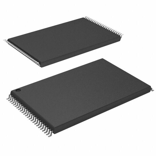


 工商网监
湘ICP备2023018690号
工商网监
湘ICP备2023018690号
